
Precursors used in Atomic Layer Deposition CVD ALD
- Slides: 53
Precursors used in Atomic Layer Deposition /CVD ALD, CVD and Nanomaterials applications Nigel Matthews
Agenda • Who we are • Brief overview ALD, materials & applications • A CVD application and comparison with ALD • A few Nanomaterials & applications
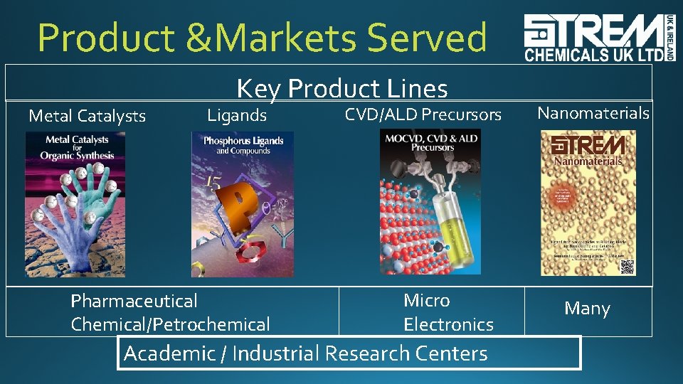
Product &Markets Served Metal Catalysts Key Product Lines Ligands Pharmaceutical Chemical/Petrochemical CVD/ALD Precursors Micro Electronics Academic / Industrial Research Centers Nanomaterials Many
Strem Product Line History: • 1965 – Metal carbonyls, initially for chemical synthesis • 1984 – Electronic chemicals (MOCVD) • 2004 - Nanomaterials • 2012 - Metal Organic Frameworks (MOFs)
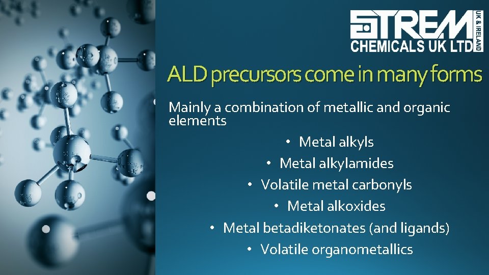
ALD precursors come in many forms Mainly a combination of metallic and organic elements • Metal alkylamides • Volatile metal carbonyls • Metal alkoxides • Metal betadiketonates (and ligands) • Volatile organometallics
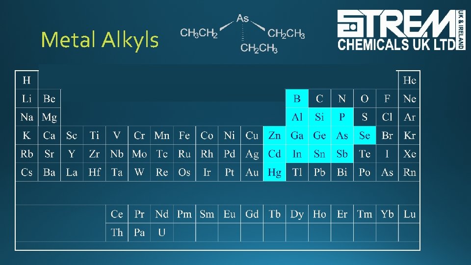
Metal Alkyls
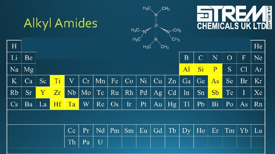
Alkyl Amides
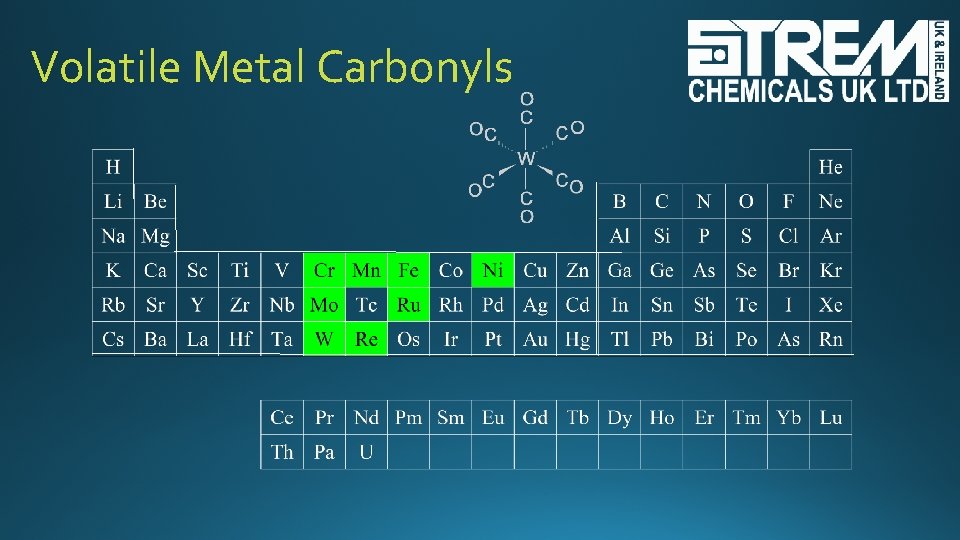
Volatile Metal Carbonyls
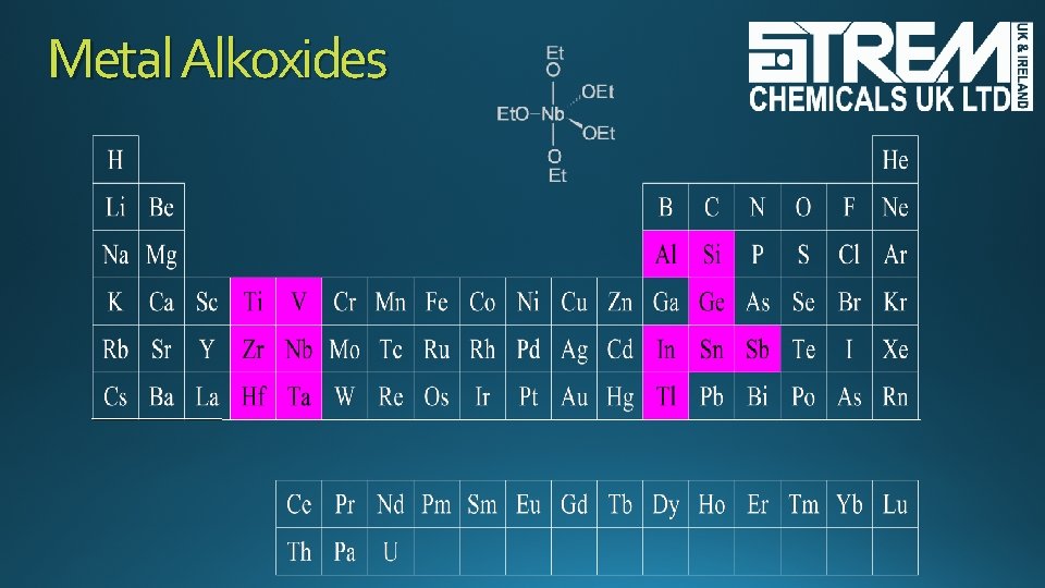
Metal Alkoxides
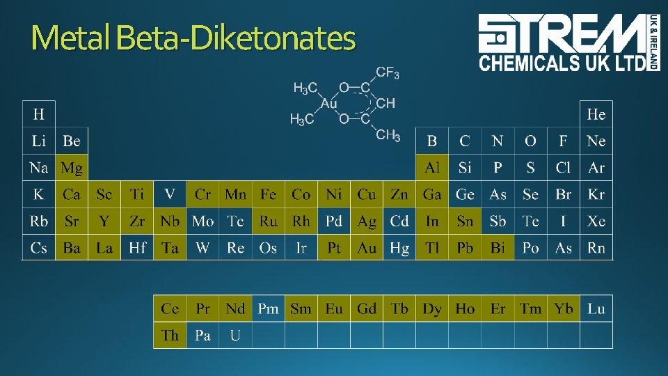
Metal Beta-Diketonates
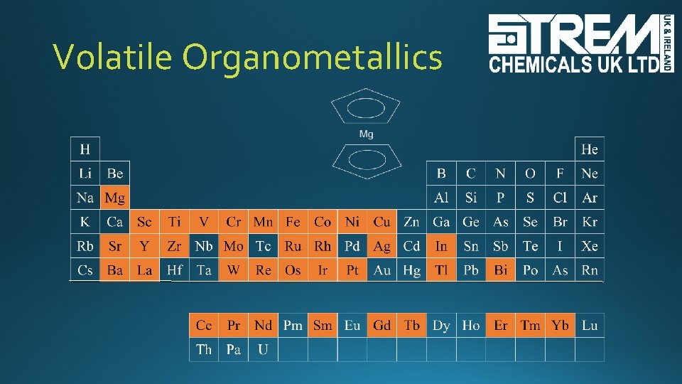
Volatile Organometallics
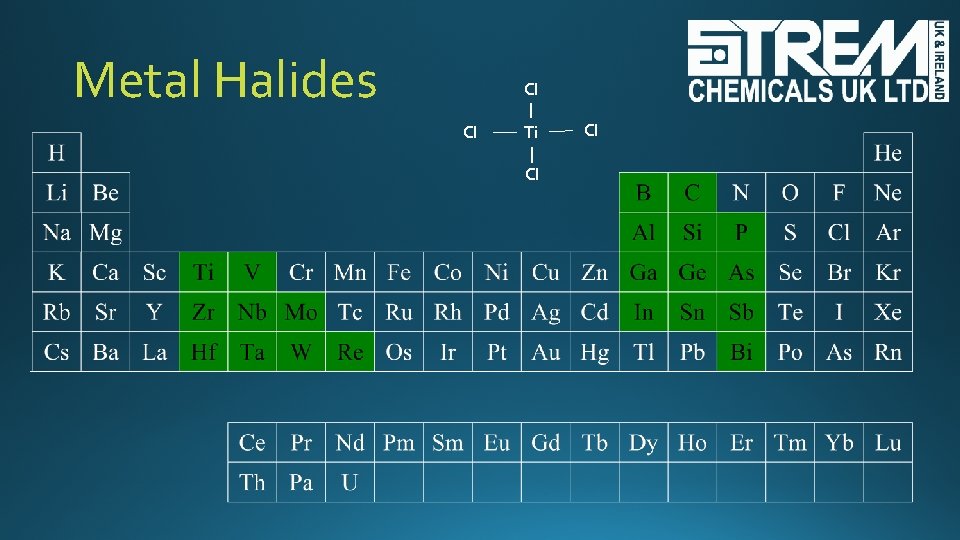
Metal Halides Cl Cl Ti Cl Cl
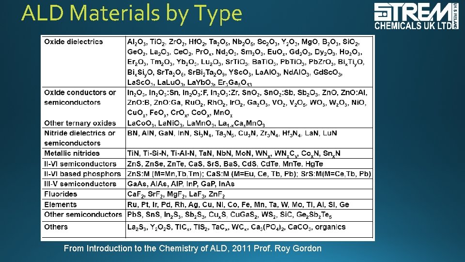
ALD Materials by Type From Introduction to the Chemistry of ALD, 2011 Prof. Roy Gordon
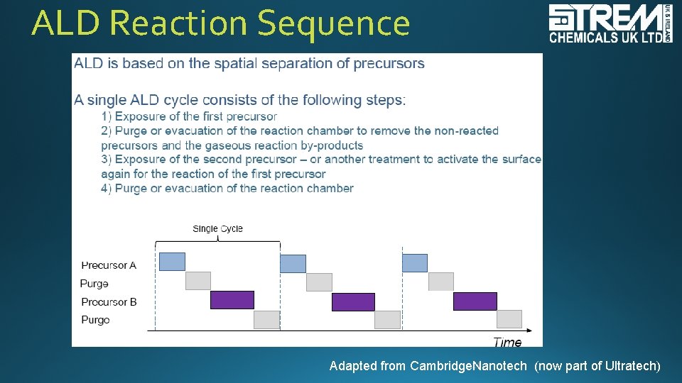
ALD Reaction Sequence 14 Adapted from Cambridge. Nanotech (now part of Ultratech)
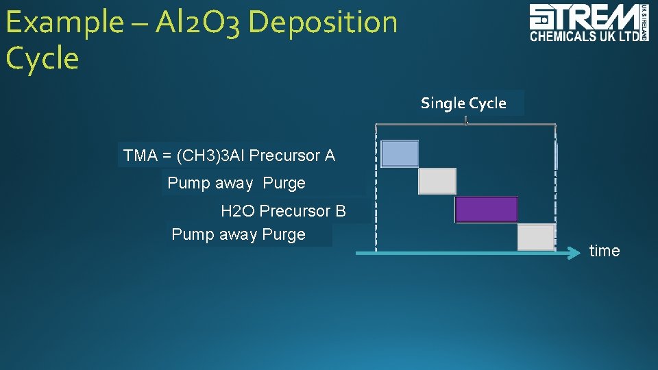
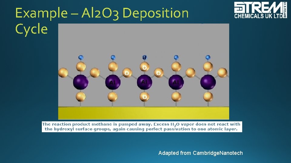
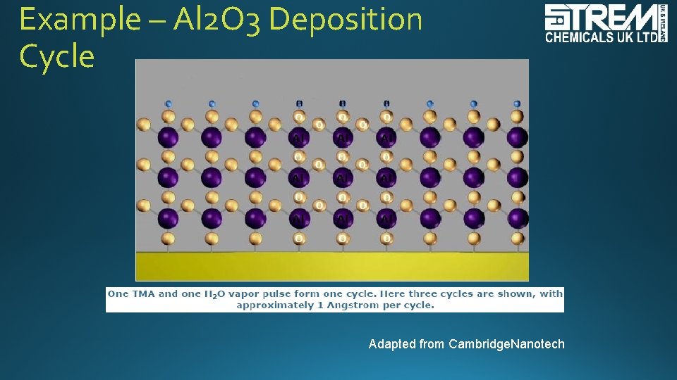
Example – Al 2 O 3 Deposition Cycle Single Cycle TMA = (CH 3)3 Al Precursor A Pump away Purge H 2 O Precursor B Pump away Purge time
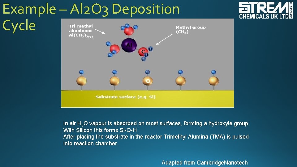
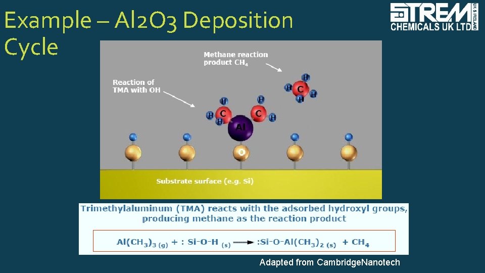
Example – Al 2 O 3 Deposition Cycle In air H 2 O vapour is absorbed on most surfaces, forming a hydroxyle group With Silicon this forms Si-O-H After placing the substrate in the reactor Trimethyl Alumina (TMA) is pulsed into reaction chamber. Adapted from Cambridge. Nanotech
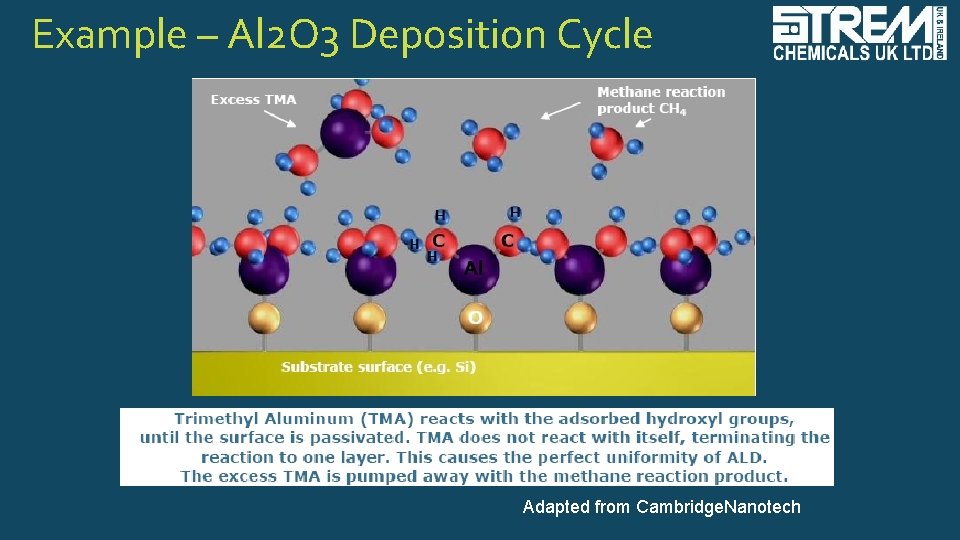
Example – Al 2 O 3 Deposition Cycle Adapted from Cambridge. Nanotech
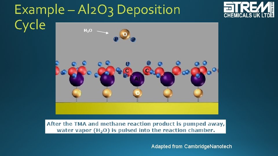
Example – Al 2 O 3 Deposition Cycle Adapted from Cambridge. Nanotech
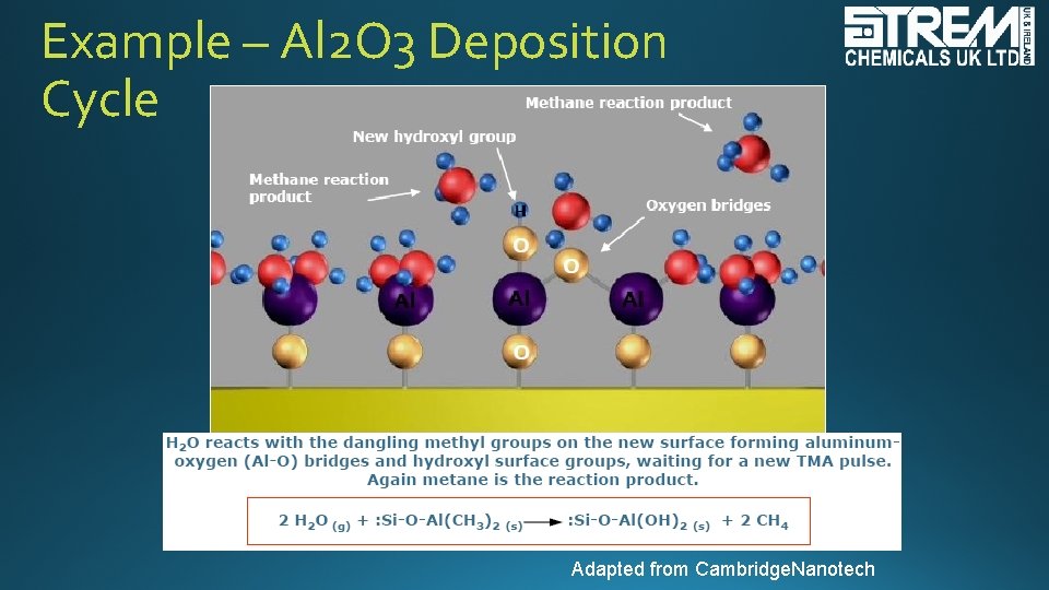
Example – Al 2 O 3 Deposition Cycle Adapted from Cambridge. Nanotech
Example – Al 2 O 3 Deposition Cycle Adapted from Cambridge. Nanotech
Example – Al 2 O 3 Deposition Cycle Adapted from Cambridge. Nanotech
Example – Al 2 O 3 Deposition Cycle Adapted from Cambridge. Nanotech
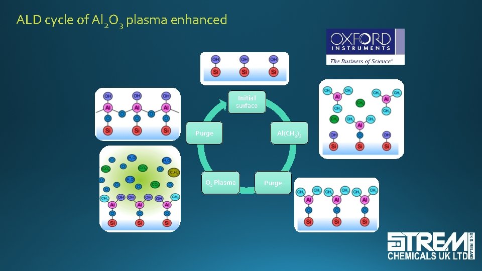
ALD cycle of Al 2 O 3 plasma enhanced Initial surface Purge O 2 Plasma Al(CH 3)3 Purge
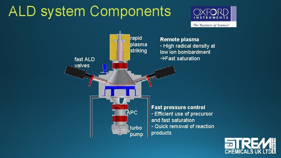
ALD system Components rapid plasma striking fast ALD valves APC turbo pump Remote plasma • High radical density at low ion bombardment Fast saturation Fast pressure control • Efficient use of precursor and fast saturation • Quick removal of reaction products
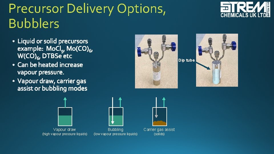
Precursor Delivery Options, Bubblers Dip tube Vapour draw Bubbling Carrier gas assist (high vapour pressure liquids) (low vapour pressure liquids) (solids)
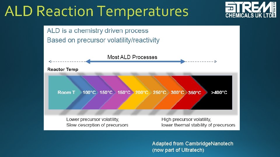
ALD Reaction Temperatures Adapted from Cambridge. Nanotech (now part of Ultratech)
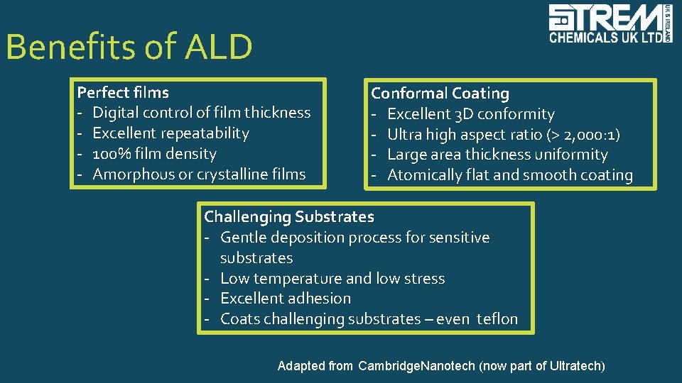
Benefits of ALD Perfect films - Digital control of film thickness - Excellent repeatability - 100% film density - Amorphous or crystalline films Conformal Coating - Excellent 3 D conformity - Ultra high aspect ratio (> 2, 000: 1) - Large area thickness uniformity - Atomically flat and smooth coating Challenging Substrates - Gentle deposition process for sensitive substrates - Low temperature and low stress - Excellent adhesion - Coats challenging substrates – even teflon Adapted from Cambridge. Nanotech (now part of Ultratech)
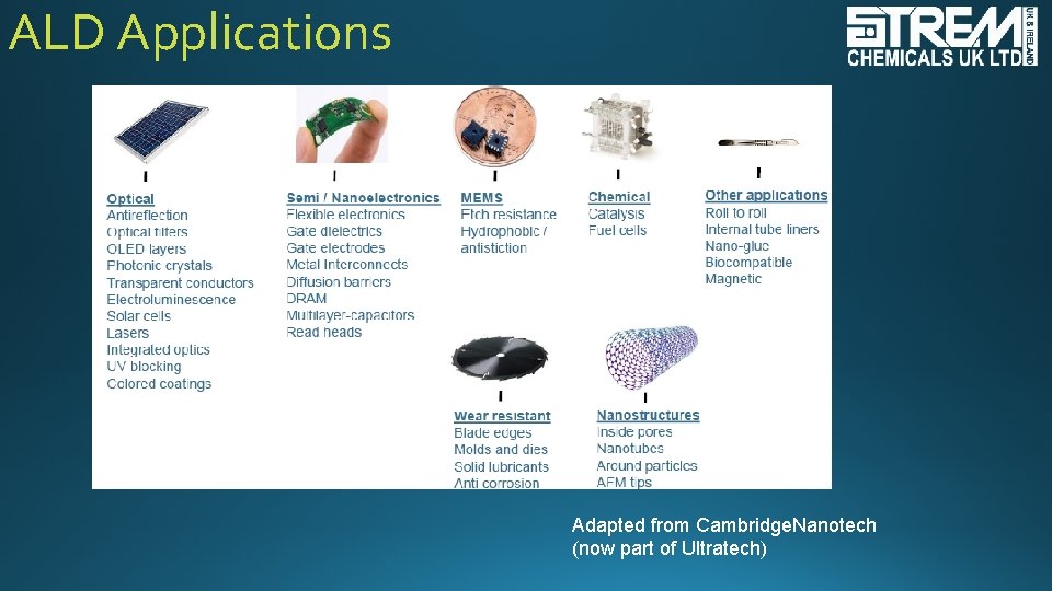
ALD Applications Adapted from Cambridge. Nanotech (now part of Ultratech)
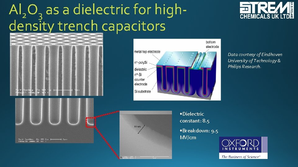
Al 2 O 3 as a dielectric for highdensity trench capacitors Data courtesy of Eindhoven University of Technology & Philips Research. • Dielectric constant: 8. 5 • Breakdown: 9. 5 MV/cm
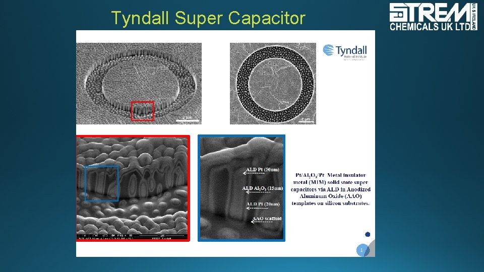
Tyndall Super Capacitor
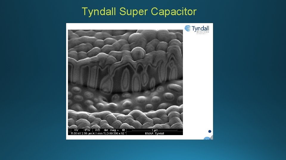
Tyndall Super Capacitor
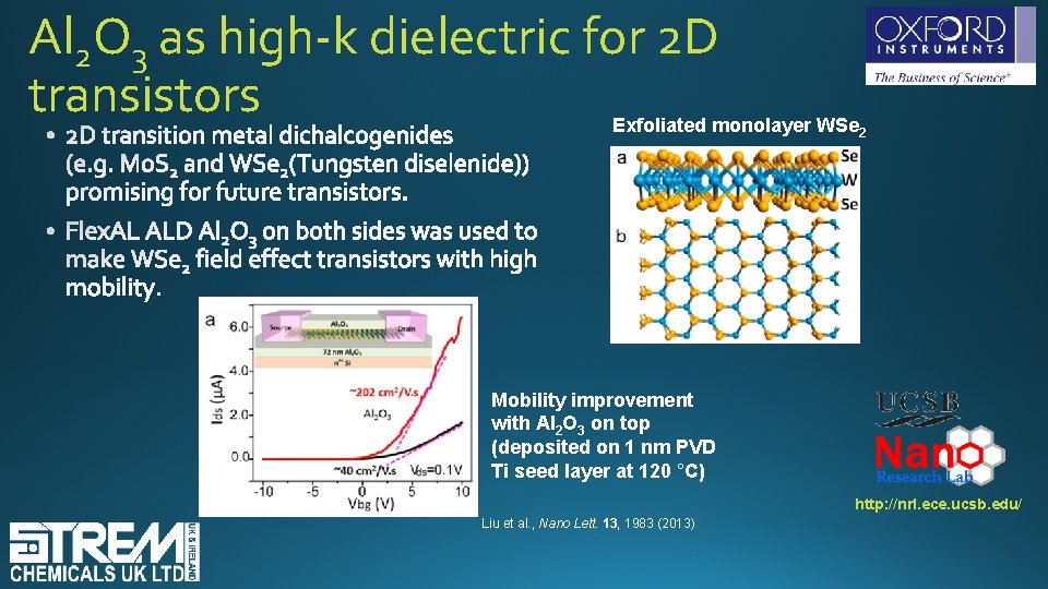
Al 2 O 3 as high-k dielectric for 2 D transistors Exfoliated monolayer WSe 2 Mobility improvement with Al 2 O 3 on top (deposited on 1 nm PVD Ti seed layer at 120 °C) http: //nrl. ece. ucsb. edu/ Liu et al. , Nano Lett. 13, 1983 (2013)
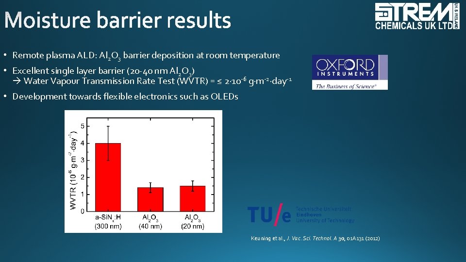
• Remote plasma ALD: Al 2 O 3 barrier deposition at room temperature • Excellent single layer barrier (20 -40 nm Al 2 O 3) Water Vapour Transmission Rate Test (WVTR) = ≤ 2· 10 -6 g·m-2·day-1 • Development towards flexible electronics such as OLEDs Keuning et al. , J. Vac. Sci. Technol. A 30, 01 A 131 (2012)
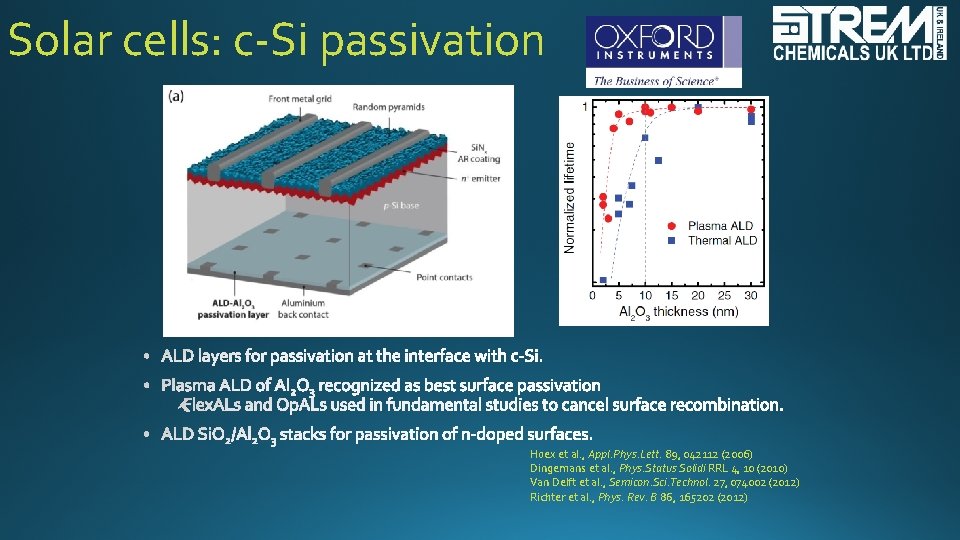
Solar cells: c-Si passivation Hoex et al. , Appl. Phys. Lett. 89, 042112 (2006) Dingemans et al. , Phys. Status Solidi RRL 4, 10 (2010) Van Delft et al. , Semicon. Sci. Technol. 27, 074002 (2012) Richter et al. , Phys. Rev. B 86, 165202 (2012)
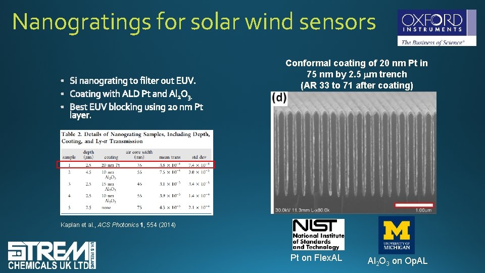
Nanogratings for solar wind sensors Conformal coating of 20 nm Pt in 75 nm by 2. 5 mm trench (AR 33 to 71 after coating) Kaplan et al. , ACS Photonics 1, 554 (2014) Pt on Flex. AL Al 2 O 3 on Op. AL
Chemical Vapour Deposition
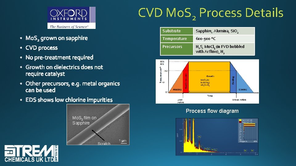
CVD Mo. S 2 Process Details Substrate Sapphire, Alumina, Si. O 2 Temperature 600 -900 ºC Precursors H 2 S, Mo. Cl 5 (in FVD bubbled with Ar flow), H 2 Process flow diagram Mo. S 2 film on Sapphire EDS: Presence of Mo, S and very low/no Cl Scratch
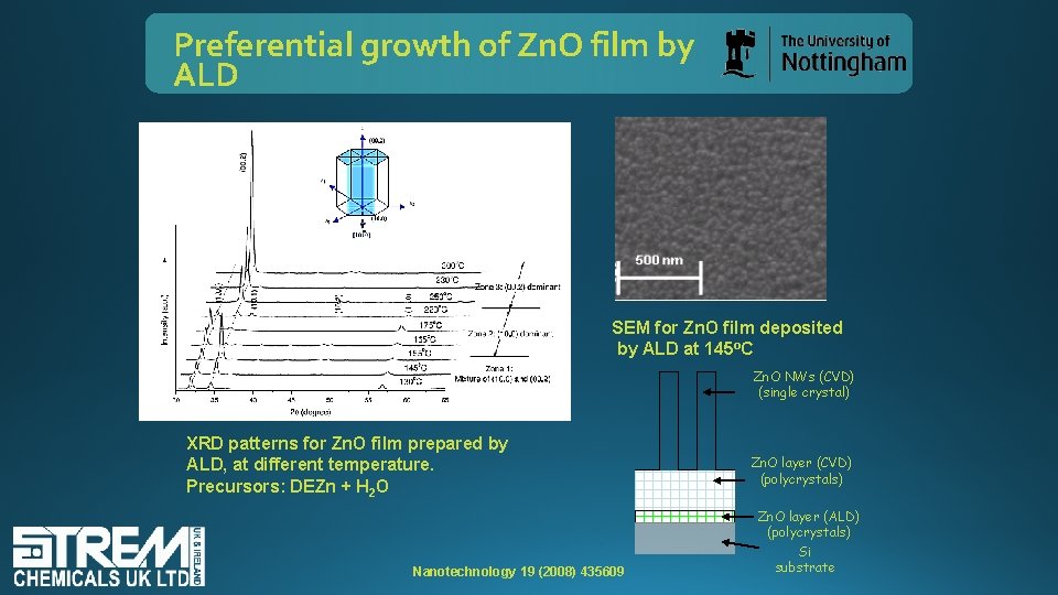
Preferential growth of Zn. O film by ALD SEM for Zn. O film deposited by ALD at 145 o. C Zn. O NWs (CVD) (single crystal) XRD patterns for Zn. O film prepared by ALD, at different temperature. Precursors: DEZn + H 2 O Nanotechnology 19 (2008) 435609 Zn. O layer (CVD) (polycrystals) Zn. O layer (ALD) (polycrystals) Si substrate
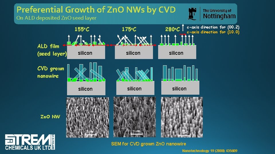
Preferential Growth of Zn. O NWs by CVD On ALD deposited Zn. O seed layer 155 o. C ALD film (seed layer) 175 o. C silicon c-axis direction for (00. 2) c-axis direction for (10. 0) 280 o. C silicon CVD grown nanowire silicon Zn. O NW SEM for CVD grown Zn. O nanowire Nanotechnology 19 (2008) 435609
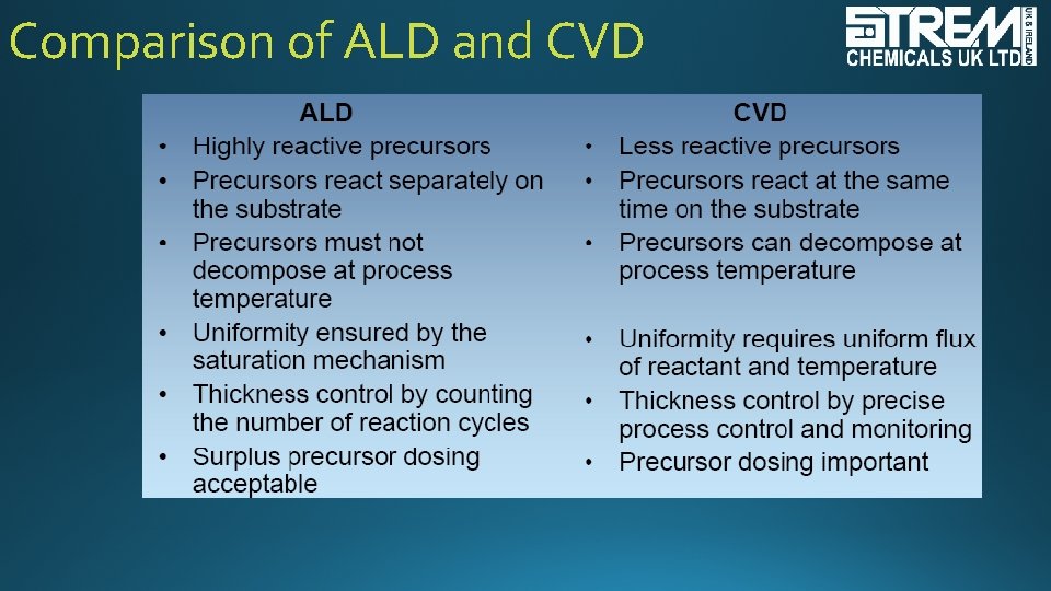
Comparison of ALD and CVD
Nanomaterials
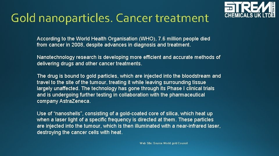
Gold nanoparticles. Cancer treatment According to the World Health Organisation (WHO), 7. 6 million people died from cancer in 2008, despite advances in diagnosis and treatment. Nanotechnology research is developing more efficient and accurate methods of delivering drugs and other cancer treatments. The drug is bound to gold particles, which are injected into the bloodstream and travel to the site of the tumour, treating it while leaving surrounding tissue largely unaffected. The technology has gone through its Phase I clinical trials and is undergoing further testing in collaboration with the pharmaceutical company Astra. Zeneca. Use of “nanoshells”, consisting of a gold-coated core of silica, which heat up when a laser light of a specific frequency is directed at them. These particles are injected into the tumour, which is then illuminated with a near-infrared laser, destroying the cancer cells with heat. Web Site: Source World gold Council
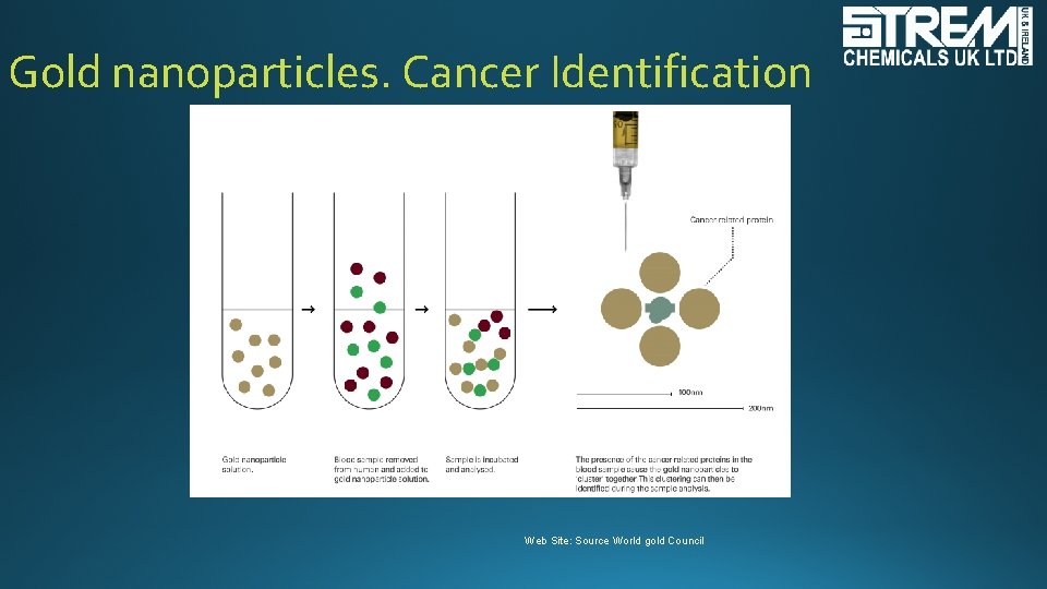
Gold nanoparticles. Cancer Identification Web Site: Source World gold Council
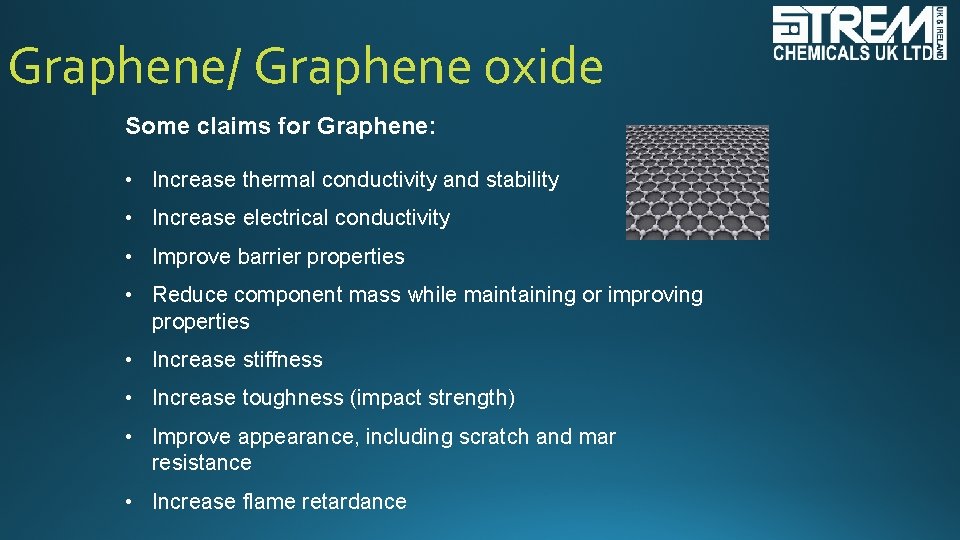
Graphene/ Graphene oxide Some claims for Graphene: • Increase thermal conductivity and stability • Increase electrical conductivity • Improve barrier properties • Reduce component mass while maintaining or improving properties • Increase stiffness • Increase toughness (impact strength) • Improve appearance, including scratch and mar resistance • Increase flame retardance
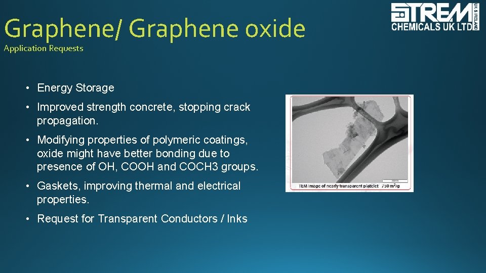
Graphene/ Graphene oxide Application Requests • Energy Storage • Improved strength concrete, stopping crack propagation. • Modifying properties of polymeric coatings, oxide might have better bonding due to presence of OH, COOH and COCH 3 groups. • Gaskets, improving thermal and electrical properties. • Request for Transparent Conductors / Inks
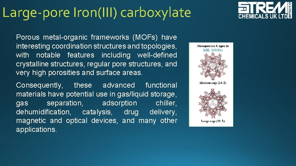
Large-pore Iron(III) carboxylate Porous metal-organic frameworks (MOFs) have interesting coordination structures and topologies, with notable features including well-defined crystalline structures, regular pore structures, and very high porosities and surface areas. Consequently, these advanced functional materials have potential use in gas/liquid storage, gas separation, adsorption chiller, dehumidification, catalysis, drug delivery, magnetic and optical devices, and many other applications.
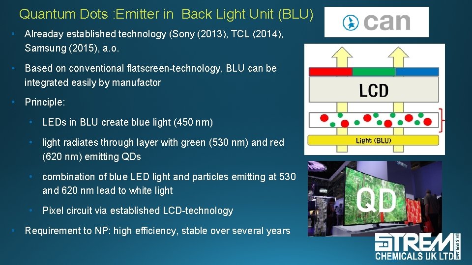
Quantum Dots : Emitter in Back Light Unit (BLU) • Alreaday established technology (Sony (2013), TCL (2014), Samsung (2015), a. o. • Based on conventional flatscreen-technology, BLU can be integrated easily by manufactor • Principle: • LEDs in BLU create blue light (450 nm) • light radiates through layer with green (530 nm) and red (620 nm) emitting QDs • combination of blue LED light and particles emitting at 530 and 620 nm lead to white light • Pixel circuit via established LCD-technology • Requirement to NP: high efficiency, stable over several years 52
Acknowledgements CAN Gmb. H- Katharina Poulsen Nottingham Uni - Fang Xu Oxford Instruments – Knoops Ravi Sundaram Harm Picosun / Sis. TEM Technology – Malcolm Rowntree Strem Inc/Ultra Tech – Tyndall - Ephraim Honig Alan Blake Michael Burke