Power Point Slides The Processor Language Design of


![Register File Read is. Ret ra(15) rs 1 inst[19: 22] inst 1 A read Register File Read is. Ret ra(15) rs 1 inst[19: 22] inst 1 A read](https://slidetodoc.com/presentation_image_h/20a0c446370b8123290fc0e245cdd058/image-18.jpg)

![Immediate and Branch Unit imm inst[1: 18] pc inst 27 18 calculate immediate shift Immediate and Branch Unit imm inst[1: 18] pc inst 27 18 calculate immediate shift](https://slidetodoc.com/presentation_image_h/20a0c446370b8123290fc0e245cdd058/image-20.jpg)


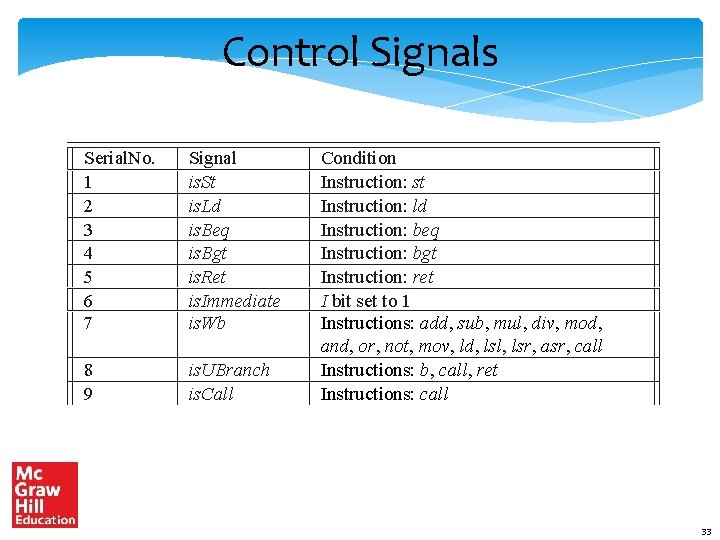
![The Ha rdwired Control Unit opcode inst[28: 32] I bit inst[27] Control unit control The Ha rdwired Control Unit opcode inst[28: 32] I bit inst[27] Control unit control](https://slidetodoc.com/presentation_image_h/20a0c446370b8123290fc0e245cdd058/image-32.jpg)








- Slides: 71

Power. Point Slides The Processor Language Design of Bits Computer Organisation and Architecture Smruti Ranjan Sarangi, IIT Delhi Chapter 8 Processor Design PROPRIETARY MATERIAL. © 2014 The Mc. Graw-Hill Companies, Inc. All rights reserved. No part of this Power. Point slide may be displayed, reproduced or distributed in any form or by any means, without the prior written permission of the publisher, or used beyond the limited distribution to teachers and educators permitted by Mc. Graw-Hill for their individual course preparation. Power. Point Slides are being provided only to authorized professors and instructors for use in preparing for classes using the affiliated textbook. No other use or distribution of this Power. Point slide is permitted. The Power. Point slide may not be sold and may not be distributed or be used by any student or any other third party. No part of the slide may be reproduced, displayed or distributed in any form or by any means, electronic or otherwise, without the prior written permission of Mc. Graw Hill Education (India) Private Limited. 1

These slides are meant to be used along with the book: Computer Organisation and Architecture, Smruti Ranjan Sarangi, Mc. Graw. Hill 2015 Visit: http: //www. cse. iitd. ernet. in/~srsarangi/archbooksoft. html 2

Outline * Overview of a Processor * Detailed Design of each Stage * The Control Unit * Microprogrammed Processor * Microassembly Language * The Microcontrol Unit 3

Processor Design * The aim of processor design * Implement the entire Simple. Risc ISA * Process the binary format of instructions * Provide as much of performance as possible * Basic Approach * Divide the processing into stages * Design each stage separately 4

A Car Assembly Line * Similar to a car assembly line * Cast raw metal into the chassis of a car * Build the Engine * Assemble the engine and the chassis * Place the dashboard, and upholstery 5

A Processor Divided Into Stages Instruction Fetch (IF) Operand Fetch (OF) Execute (EX) Memory Access (MA) Register Write (RW) * Instruction Fetch (IF) * Fetch an instruction from the instruction memory * Compute the address of the next instruction 6

Operand Fetch (OF) Stage * Operand Fetch (OF) * Decode the instruction (break it into fields) * Fetch the register operands from the register file * Compute the branch target (PC + offset) * Compute the immediate (16 bits + 2 modifiers) * Generate control signals (we will see later) 7

Execute (EX) Stage * The EX Stage * Contains an Arithmetic-Logical Unit (ALU) * This unit can perform all arithmetic operations ( add, sub, mul, div, cmp, mod), and logical operations (and, or, not) * Contains the branch unit for computing the branch condition (beq, bgt) * Contains the flags register (updated by the cmp instruction) 8

MA and RW Stages * MA (Memory Access) Stage * Interfaces with the memory system * Executes a load or a store * RW (Register Write) Stage * Writes to the register file * In the case of a call instruction, it writes the return address to register, ra 9

Outline * Outline of a Processor * Detailed Design of each Stage * The Control Unit * Microprogrammed Processor * Microassembly Language * The Microcontrol Unit 10

Instruction Fetch (IF) Stage Fetch unit is. Branch. Taken 32 32 1 branch. PC 0 4 pc 32 32 inst triggered by a negative clock edge Instruction memory 1 0 1 - input 1 0 - input 0 Multiplexer control signal 11

The Fetch unit * The pc register contains the program counter (negative edge triggered) * We use the pc to access the instruction memory * The multiplexer chooses between * pc + 4 * branch. Target * It uses a control signal → is. Branch. Taken 12

is. Branch. Taken * is. Branch. Taken is a control signal * It is generated by the EX unit * Conditions on is. Branch. Taken Instruction non-branch instruction call ret b beq bgt Value of is. Branch. Taken 0 1 1 1 branch taken – 1 branch not taken – 0 13

Data Path and Control Path * The data path consists of all the elements in a processor that are dedicated to storing, retrieving, and processing data such as register files, memory, and the ALU. * The control path primarily contains the control unit, whose role is to generate the appropriate signals to control the movement of instructions, and data in the data path. 14

Control Path Control path Interconnection network Data path elements We will currently look at the hardwired control path. 15

Operand Fetch Unit Inst. add sub mul div mod cmp and or not mov Code 000001 00010 00011 00100 00101 00110 00111 01000 01001 Format add rd, rs 1, (rs 2/imm) sub rd, rs 1, (rs 2/imm) mul rd, rs 1, (rs 2/imm) div rd, rs 1, (rs 2/imm) mod rd, rs 1, (rs 2/imm) cmprs 1, (rs 2/imm) and rd, rs 1, (rs 2/imm) or rd, rs 1, (rs 2/imm) not rd, (rs 2/imm) mov rd, (rs 2/imm) Inst. lsl lsr asr nop ld st beq bgt b call ret Code 01010 01011 01100 01101 01110 01111 10000 10001 10010 10011 10100 Format lsl rd, rs 1, (rs 2/imm) lsr rd, rs 1, (rs 2/imm) asr rd, rs 1, (rs 2/imm) nop ld rd, imm[rs 1] st rd, imm[rs 1] beq offset bgt offset b offset call offset ret 16

Instruction Formats Format Definition branch op (28 -32) offset (1 -27) register rd (23 -26) rs 1 (19 -22) rs 2 (15 -18) op (28 -32) I (27) immediate op (28 -32) I (27) rd (23 -26) rs 1 (19 -22) imm (1 -18) op → opcode, offset → branch offset, I → immediate bit, rd → destination register rs 1 → source register 1, rs 2 → source register 2, imm → immediate operand * Each format needs to be handled separately. 17
![Register File Read is Ret ra15 rs 1 inst19 22 inst 1 A read Register File Read is. Ret ra(15) rs 1 inst[19: 22] inst 1 A read](https://slidetodoc.com/presentation_image_h/20a0c446370b8123290fc0e245cdd058/image-18.jpg)
Register File Read is. Ret ra(15) rs 1 inst[19: 22] inst 1 A read port 1 D op 1 0 rd inst[23: 26] 1 A rs 2 inst[15: 18] 0 is. St read port 2 Register file D op 2 A address D data * First input → rs 1 or ra(15) (ret instruction) * Second input → rs 2 or rd (store instruction) 18

Register File Access * The register file has two read ports * 1 st Input * 2 nd Input * The two outputs are op 1, and op 2 * op 1 is the branch target (return address) in the case of a ret instruction, or rs 1 * op 2 is the value that needs to be stored in the case of a store instruction, or rs 2 19
![Immediate and Branch Unit imm inst1 18 pc inst 27 18 calculate immediate shift Immediate and Branch Unit imm inst[1: 18] pc inst 27 18 calculate immediate shift](https://slidetodoc.com/presentation_image_h/20a0c446370b8123290fc0e245cdd058/image-20.jpg)
Immediate and Branch Unit imm inst[1: 18] pc inst 27 18 calculate immediate shift by 2 bits and extend sign 32 32 immx branch. Target * Compute immx (extended immediate), branch. Target, irrespective of the instruction format. * For the branch. Target we need to choose between the embedded target and op 1 (ret) 20

OF Unit Execute Operand fetch unit Fetch unit (opcode, I bit) inst 18 inst[1: 18] calculate immediate shift by 2 bits and extend sign 27 ra(15) A read port 1 inst[15: 18] D op 1 0 rd rs 2 branch. Target 32 is. Ret inst[19: 22] inst[23: 26] immx 32 1 rs 1 reg. operands pc imm. operands inst[27: 32] imm unit Control unit 6 D 1 op 2 A read port 2 0 is. St Register file A D address data 21

EX Stage – Branch Unit from OF branch. PC branch. Target op 1 0 1 is. Ret is. Branch. Taken is. Beq is. UBranch flags. E is. Bgt flags. GT flags Generates the is. Branch. Taken Signal 22

ALU and mem insts op 1 immx op 2 1 A B ALU (Arithmetic logic unit) alu. Result 0 s is. Immediate alu. Signals Choose between immx and op 2 based on the value of the I bit 23

Inside the ALU is. Lsl is. Sub is. Add is. Ld is. St is. Asr is. Cmp A Shift unit flags A B is. Lsr B Adder is. Or is. Not is. And is. Mul A B Multiplier is. Div Logical unit is. Mod A B is. Mov A B Divider Mov B alu. Result 24

Disabling some Inputs * We do not want all the units of the ALU to be active at the same time because of we want to save power * The instruction will only use 1 unit * Power is dissipated when the inputs or outputs make a transition (0 → 1, 1 → 0) * We shall avoid a transition by not letting the new inputs to propagate to units that do not require them * They will thus have the old inputs (no switching) 25

Use a Transmission Gate S S * output = input (if S = 1) * Otherwise, the output is totally disconnected from the input 26

EX Unit Execute unit branch. PC from OF is. Branch. Taken branch. Target op 1 0 1 is. Ret is. UBranch is. Beq flags. E is. Bgt flags. GT flags ALU and mem insts op 1 immx op 2 1 A B ALU (Arithmetic logic unit) alu. Result 0 s is. Immediate alu. Signals 27

MA Unit is. Ld 32 op 2 is. St mdr 32 Memory unit 32 alu. Result ld. Result mar mdr memory data reg. mar memory address reg. Data memory 28

RW Unit register writeback unit Register file A read port 1 D E write port A read port 2 D 32 alu. Result 32 ld. Result 32 pc is. Wb A D rd (inst[23: 26]) 0 is. Call 00 result 01 E A 10 4 ra(15) 1 D is. Ld enable address data is. Call 29

1 pc + 4 pc 0 Instruction memory Control unit Instruction rd rs 2 0 1 rs 1 ra(15) is. Ret 0 1 is. St data Register file Immediate and branch target reg op 1 op 2 is. Wb immx 01 is. Immediate 0 1 is. Ret alu. Signals A B flags is. Branch. Taken ALU mar mdr Branch unit is. Ld Memory unit Data memory i s. B e q is Bgt is U B ra n c h is. St pc 4 10 01 is. Ld 00 is. Call rd data ra(15) 0 1 30

Outline * Outline of a Processor * Detailed Design of each Stage * The Control Unit * Microprogrammed Processor * Microassembly Language * The Microcontrol Unit 31
![The Ha rdwired Control Unit opcode inst28 32 I bit inst27 Control unit control The Ha rdwired Control Unit opcode inst[28: 32] I bit inst[27] Control unit control](https://slidetodoc.com/presentation_image_h/20a0c446370b8123290fc0e245cdd058/image-32.jpg)
The Ha rdwired Control Unit opcode inst[28: 32] I bit inst[27] Control unit control signals * Given the opcode and the immediate bit * It generates all the control signals 32

Control Signals Serial. No. 1 2 3 4 5 6 7 Signal is. St is. Ld is. Beq is. Bgt is. Ret is. Immediate is. Wb 8 9 is. UBranch is. Call Condition Instruction: st Instruction: ld Instruction: beq Instruction: bgt Instruction: ret I bit set to 1 Instructions: add, sub, mul, div, mod, and, or, not, mov, ld, lsl, lsr, asr, call Instructions: b, call, ret Instructions: call 33

Control Signals – II alu. Signal 10 11 12 13 14 15 16 17 18 19 20 21 22 is. Add is. Sub is. Cmp is. Mul is. Div is. Mod is. Lsl is. Lsr is. Asr is. Or is. And is. Not is. Mov Instructions: add, ld, st Instruction: sub Instruction: cmp Instruction: mul Instruction: div Instruction: mod Instruction: lsl Instruction: lsr Instruction: asr Instruction: or Instruction: and Instruction: not Instruction: mov 34

Control signal Logic opcode immediate bit op 5 op 45 op 3 op 2 op 1 I Serial No. 1 2 3 4 5 6 7 Signal is. St is. Ld is. Beq is. Bgt is. Ret is. Immediate is. Wb 8 9 is. Ubranch is. Call Condition op 5. op 4. op 3. op 2. op 1 I ~(op 5 + op 5. op 3. op 1. (op 4 + op 2)) + op 5. op 4. op 3. op 2. op 1 op 5. op 4. (op 3. op 2 + op 3. op 2. op 1) op 5. op 4. op 3. op 2. op 1 35

Control Signal Logic - II is. Add is. Sub is. Cmp is. Mul is. Div is. Mod is. Lsl is. Lsr is. Asr is. Or is. And is. Not is. Mov alu. Signals op 5. op 4. op 3. op 2. op 1 + op 5. op 4. op 3. op 2. op 1 op 5. op 4. op 3. op 2. op 1 36

Outline * Outline of a Processor * Detailed Design of each Stage * The Control Unit * Microprogrammed Processor * Microassembly Language * The Microcontrol Unit 37

Microprogramming * Idea of microprogramming * Expose the elements in a processor to software * Implement instructions as dedicated software routines * Why make the implementation of instructions flexible ? * Dynamically change their behaviour * Fix bugs in implementations * Implement very complex instructions 38

Microprogrammed Data Path * Expose all the state elements to dedicated system software – firmware * Write dedicated routines in firmware for implementing each instruction * Basic idea * 1 Simple. Risc Instruction → Several micro instructions * Execute each micro instruction * We require a microprogram counter, and microinstruction memory 39

Fetch Unit pc Instruction memory ir Shared bus * The pc is used to access the instruction memory. * The contents of the instruction are saved in the instruction register (ir) 40

Decode Unit pc ir I rd rs 1 rs 2 Immediate unit immx calc. offset branch. Target Shared bus * Divide the contents of ir into different fields * I, rd, rs 1, rs 2, immx, and branch. Target 41

The Register File reg. Val reg. Data args Shared bus reg. Src Register file * reg. Src (id of the source/dest register) * reg. Data (data to be stored) * reg. Val (register value) 42

ALU alu. Result A args Shared bus B flags. E ALU flags. GT flags * A, B → ALU operands * args → ALU operation type * alu. Result → ALU Result 43

Memory Unit ld. Result mar args Shared bus mdr Data memory 44

Microprogrammed Data Path μ control unit opcode pc ir Instruction memory I rd rs 1 rs 2 Immediate unit immx calc. offset branch. Target mdr Data memory alu. Result A ALU B flags. E flags. GT flags reg. Val reg. Data args mar args ld. Result args Shared bus reg. Src Register file 45

Outline * Outline of a Processor * Detailed Design of each Stage * The Control Unit * Microprogrammed Processor * Microassembly Language * The Microcontrol Unit 46

Internal Registers Serial. No. Register 1 2 3 4 5 6 7 pc ir I rd rs 1 rs 2 immx Size (bits) 32 32 1 4 4 4 32 8 branch. Target 32 9 reg. Src 4 10 reg. Data 32 Function program counter instruction register immediate bit in the instruction destination register id id of the first source register id of the second source register immediate embedded in the instruction (after processing modifiers) branch target, computed as the sum of the PC and the offset embedded in the instruction contains the id of the register that needs to be accessed in the register file contains the data to be written into the register file 47

Internal Registers - II 11 12 13 14 15 16 17 18 19 reg. Val A B flags. E flags. GT alu. Result mar mdr ld. Result 32 32 32 1 1 32 32 value read from the register file first operand of the Al. U second operand of the ALU the equality flag the greater than flag the ALU result memory address register memory data register the value loaded from memory 48

Microinstructions Basic Instructions * mload. IR → Loads the instruction register (ir) with the contents of the instruction. * mdecode → Waits for 1 cycle. Meanwhile, all the decode registers get populated * mswitch → Loads the set of micro instructions corresponding to a program instruction. 49

Move Microinstructions * mmov r 1, r 2 : r 1 ← r 2 * mmov r 1, r 2, <args> : r 1 ← r 2, send the value of args on the bus * mmovi r 1, <imm> : r 1 ← imm 50

Add and Branch Microinstructions * madd r 1, imm, <args> * r 1 ← r 1 + imm * send <args> on the bus * mbeq r 1, imm, <label> * if (r 1 == imm), μpc = addr(label) * mb <label> * μpc = addr(label) 51

Summary of Microinstructions Serial. No. 1 2 3 Microinstruction mload. IR mdecode mswitch Semantics ir ← [pc] populate all the decode registers jump to the μpc corresponding to the opcode reg 1 ← reg 2, send the value of args to the unit that owns reg 1, < args > is optional reg 1 ← imm, < args > is optional 4 mmov reg 1, reg 2, < args > 5 mmovi reg 1, imm, < args > 6 madd reg 1, imm, < args > 7 mbeq reg 1, imm, < label > reg 1 ← reg 1+imm, < args > is optional if (reg 1 = imm) μpc ← addr(label) 8 mb <label> μpc ← addr(label) 52

Implementing Instructions in Microcode * The microcode preamble. begin: mload. IR mdecode madd pc, 4 mswitch * Load the program counter * Decode the instruction * Add 4 to the pc * Switch to the first microinstruction in the microcode sequence of the prog. instruction 53

3 Address Format ALU Instruction /* transfer the first operand to the ALU */ mmov reg. Src, rs 1, <read> mmov A, reg. Val /* check the value of the immediate register */ mbeq I, 1, . imm /* second operand is a register */ mmov reg. Src, rs 2, <read> mmov B, reg. Val, <aluop> mb. rw /* second operand is an immediate */. imm: mmov B, immx, <aluop> /* write the ALU result to the register file*/. rw: mmov reg. Src, rd mmov reg. Data, alu. Result, <write> mb. begin 54

The mov Instruction mov instruction /* check the value of the immediate register */ mbeq I, 1, . imm /* second operand is a register */ mmov reg. Src, rs 2, <read> mmov reg. Data, reg. Val mb. rw /* second operand is an immediate */. imm: mmov reg. Data, immx /* write to the register file*/. rw: mmov reg. Src, rd, <write> /* jump to the beginning */ mb. begin 55

The not Instruction not instruction /* check the value of the immediate register */ mbeq I, 1, . imm /* second operand is a register */ mmov reg. Src, rs 2, <read> mmov B, reg. Val, <not> /* ALU operation */ mb. rw /* second operand is an immediate */. imm: mmov B, immx, <not> /* ALU operation */ /* write to the register file*/. rw: mmov reg. Data, alu. Result mmov reg. Src, rd, <write> /* jump to the beginning */ mb. begin 56

The cmp Instruction cmp instruction /* transfer rs 1 to register A */ mov reg. Src, rs 1, <read> mov A, reg. Val /* check the value of the immediate register mbeq I, 1, . imm /* second operand is a register */ mmov reg. Src, rs 2, <read> mmov B, reg. Val, <cmp> /* ALU operation */ mb. begin /* second operand is an immediate */. imm: mmov B, immx, <cmp> /* ALU operation */ mb. begin 57

The nop Instruction * mb. begin 58

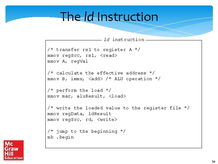
The ld Instruction ld instruction /* transfer rs 1 to register A */ mmov reg. Src, rs 1, <read> mmov A, reg. Val /* calculate the effective address */ mmov B, immx, <add> /* ALU operation */ /* perform the load */ mmov mar, alu. Result, <load> /* write the loaded value to the register file */ mmov reg. Data, ld. Result mmov reg. Src, rd, <write> /* jump to the beginning */ mb. begin 59

The st Instruction st instruction /* transfer rs 1 to register A */ mmov reg. Src, rs 1, <read> mmov A, reg. Val /* calculate the effective address */ mmov B, immx, <add> /* ALU operation */ /* perform the store */ mmov mar, alu. Result mmov reg. Src, rd, <read> mmov mdr, reg. Val, <store> /* jump to the beginning */ mb. begin 60

beq and bgt Instructions beq instruction /* test the flags register mbeq flags. E, 1, . branch mb. begin. branch: mmov pc, branch. Target mb. begin bgt instruction /* test the flags register mbeq flags. GT, 1, . branch mb. begin. branch: mmov pc, branch. Target mb. begin 61

call Instruction call instruction /* save PC + 4 in the return address register */ mmov reg. Data, pc mmovi reg. Src, 15, <write> /* branch to the function */ mmov pc, branch. Target mb. begin 62

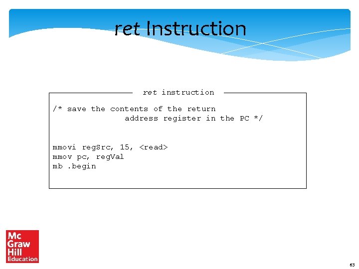
ret Instruction ret instruction /* save the contents of the return address register in the PC */ mmovi reg. Src, 15, <read> mmov pc, reg. Val mb. begin 63

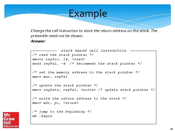
Example Change the call instruction to store the return address on the stack. The preamble need not be shown. Answer: stack based call instruction /* read the stack pointer */ mmovi reg. Src, 14, <read> madd reg. Val, -4 /* decrement the stack pointer */ /* set the memory address to the stack pointer */ mmov mar, reg. Val /* update the stack pointer */ mmov reg. Data, reg. Val, <write> /* update stack pointer */ /* write the return address to the stack */ mmov mdr, pc, <store> /* jump to the beginning */ mb. begin 64

Outline * Outline of a Processor * Detailed Design of each Stage * The Control Unit * Microprogrammed Processor * Microassembly Language * The Microcontrol Unit 65

Shared Bus Microcontrol unit µ imm is. MBranch Decode unit pc pc Read bus Write bus Reg. file, ALU, Mem unit Shared bus 66

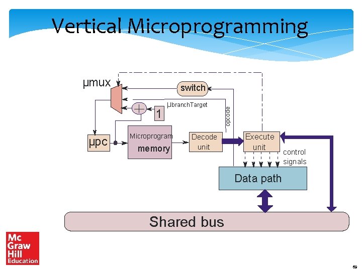
Encoding an Instruction * Vertical Microprogramming (45 bit inst. ) * * * 3 bits → type of instruction 5 bits → source register 5 bits → destination register 12 bits → immediate 10 bit → branch target in microcode memory 10 bit → args value * 3 bits → (unit id) * 7 bits → operation code 67

Horizontal Microprogramming * Encoding * 10 bits → branch target * 12 bits → immediate * 10 bits → args * 33 bits → bit vector of all the control signals * Total size of the encoded instruction : 65 bits 68

Vertical Microprogramming μmux 1 μpc μbranch. Target Microprogram memory Decode unit opcode switch Execute unit control signals Data path Shared bus 69

Horizontal Microprogramming switch μmux opcode is. MBranch M 1 μbranch. Target 1 μpc Microprogram memory control signals Execute unit Data path Shared bus 70

THE END 71