Power Optimization Toolbox for Logic Synthesis and Mapping

Power Optimization Toolbox for Logic Synthesis and Mapping Alan Mishchenko Robert Brayton UC Berkeley 1
Outline Introduction Ø Background Ø Contributions Ø l l l Sim. Switch: Switching activity estimation Power. Map: Mapping for power reduction Power. DC: Re-synthesis for power reduction Experiments Ø Conclusions Ø 2
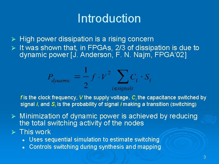
Introduction Ø Ø High power dissipation is a rising concern It was shown that, in FPGAs, 2/3 of dissipation is due to dynamic power [J. Anderson, F. N. Najm, FPGA’ 02] f is the clock frequency, V the supply voltage, Ci the capacitance switched by signal i, and Si is the probability of signal i making a transition (switching) Minimization of dynamic power is achieved by reducing the total switching activity of the nodes Ø This work Ø l l Uses sequential simulation to estimate switching Controls switching during synthesis and mapping 3
Background Ø Boolean network l Ø Technology mapping l Ø And-Inverter Graphs LUTs and standard cells SAT-based re-synthesis l Resubstitution with don’t-cares 4
AIGs: Unifying Representation Ø An underlying data structure for various computations l Ø A unifying representation for the whole synthesis/mapping/resynthesis/verification flow l l Ø Rewriting, resubstitution, simulation, SAT sweeping, induction, etc are based on the same AIG manager Synthesis, mapping, verification use the same data-structure Allows multiple structures to be stored and used for mapping The main functional representation in ABC l A foundation of “contemporary logic synthesis” 5
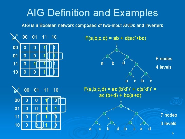
AIG Definition and Examples AIG is a Boolean network composed of two-input ANDs and inverters a cd b 00 01 11 10 00 0 0 1 1 11 0 10 0 0 1 0 F(a, b, c, d) = ab + d(ac’+bc) a 6 nodes d b 4 levels a a cd b 00 01 11 10 c b c F(a, b, c, d) = ac’(b’d’)’ + c(a’d’)’ = ac’(b+d) + bc(a+d) 00 0 0 1 1 11 0 1 1 0 7 nodes 10 0 0 1 0 3 levels a c b d b c a d 6
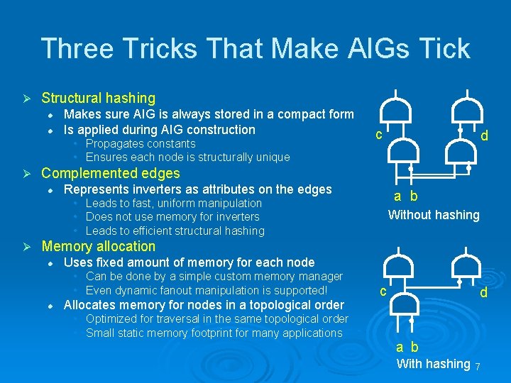
Three Tricks That Make AIGs Tick Ø Structural hashing l l Makes sure AIG is always stored in a compact form Is applied during AIG construction • Propagates constants • Ensures each node is structurally unique Ø d Complemented edges l Represents inverters as attributes on the edges • • • Ø c a b Leads to fast, uniform manipulation Does not use memory for inverters Leads to efficient structural hashing Without hashing Memory allocation l Uses fixed amount of memory for each node • Can be done by a simple custom memory manager • Even dynamic fanout manipulation is supported! l Allocates memory for nodes in a topological order • Optimized for traversal in the same topological order • Small static memory footprint for many applications c d a b With hashing 7
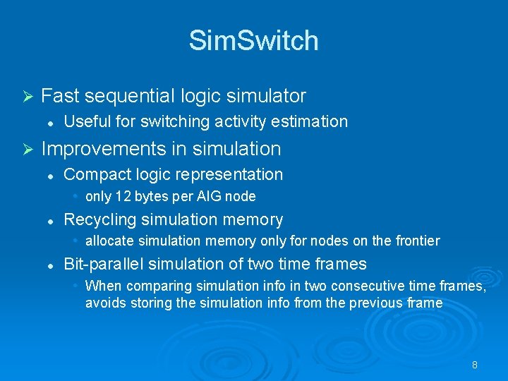
Sim. Switch Ø Fast sequential logic simulator l Ø Useful for switching activity estimation Improvements in simulation l Compact logic representation • only 12 bytes per AIG node l Recycling simulation memory • allocate simulation memory only for nodes on the frontier l Bit-parallel simulation of two time frames • When comparing simulation info in two consecutive time frames, avoids storing the simulation info from the previous frame 8
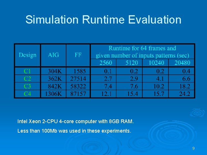
Simulation Runtime Evaluation Intel Xeon 2 -CPU 4 -core computer with 8 GB RAM. Less than 100 Mb was used in these experiments. 9
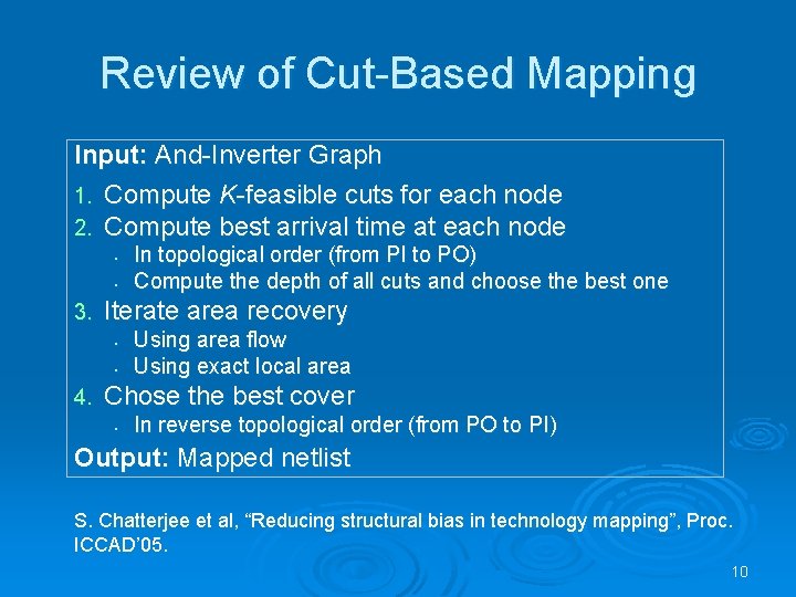
Review of Cut-Based Mapping Input: And-Inverter Graph 1. Compute K-feasible cuts for each node 2. Compute best arrival time at each node • • 3. Iterate area recovery • • 4. In topological order (from PI to PO) Compute the depth of all cuts and choose the best one Using area flow Using exact local area Chose the best cover • In reverse topological order (from PO to PI) Output: Mapped netlist S. Chatterjee et al, “Reducing structural bias in technology mapping”, Proc. ICCAD’ 05. 10
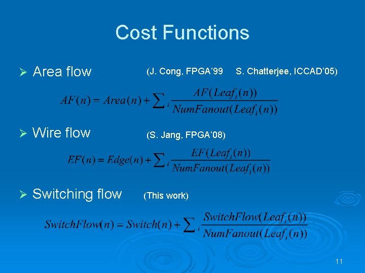
Cost Functions Ø Area flow (J. Cong, FPGA’ 99 Ø Wire flow (S. Jang, FPGA’ 08) Ø Switching flow S. Chatterjee, ICCAD’ 05) (This work) 11

Understanding a Cost-Function Flow 12
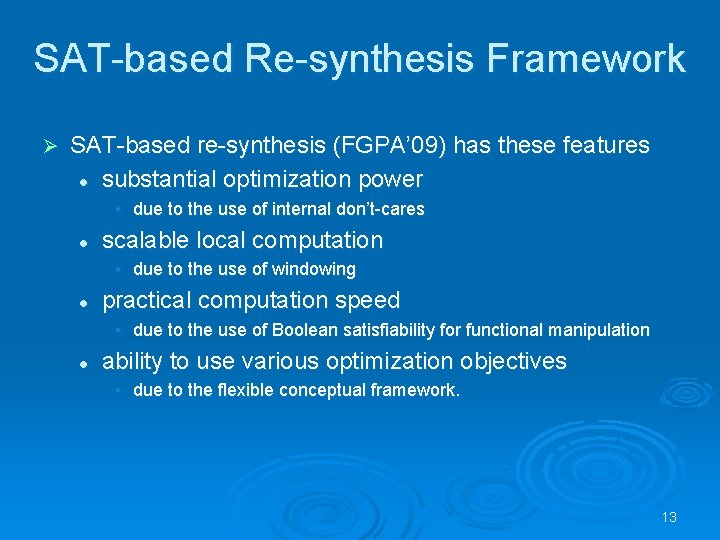
SAT-based Re-synthesis Framework Ø SAT-based re-synthesis (FGPA’ 09) has these features l substantial optimization power • due to the use of internal don’t-cares l scalable local computation • due to the use of windowing l practical computation speed • due to the use of Boolean satisfiability for functional manipulation l ability to use various optimization objectives • due to the flexible conceptual framework. 13

Two Ways to Cool Down a Hot Wire 14
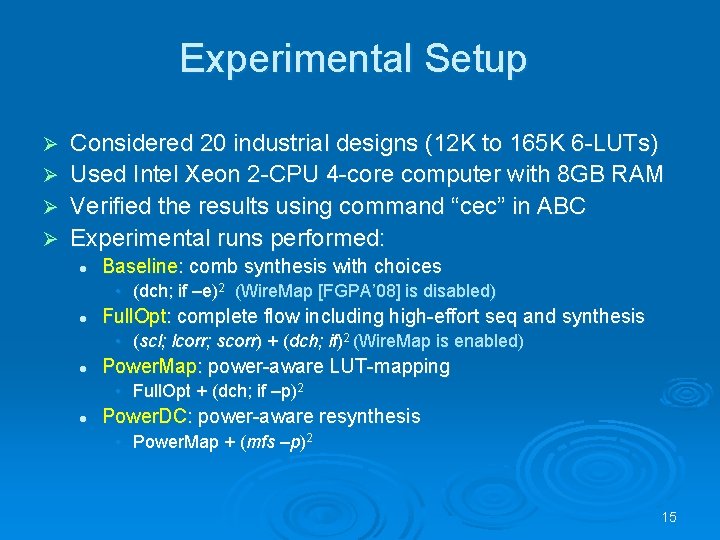
Experimental Setup Considered 20 industrial designs (12 K to 165 K 6 -LUTs) Ø Used Intel Xeon 2 -CPU 4 -core computer with 8 GB RAM Ø Verified the results using command “cec” in ABC Ø Experimental runs performed: Ø l Baseline: comb synthesis with choices • (dch; if –e)2 (Wire. Map [FGPA’ 08] is disabled) l Full. Opt: complete flow including high-effort seq and synthesis • (scl; lcorr; scorr) + (dch; if)2 (Wire. Map is enabled) l Power. Map: power-aware LUT-mapping • Full. Opt + (dch; if –p)2 l Power. DC: power-aware resynthesis • Power. Map + (mfs –p)2 15

Experimental Data 16
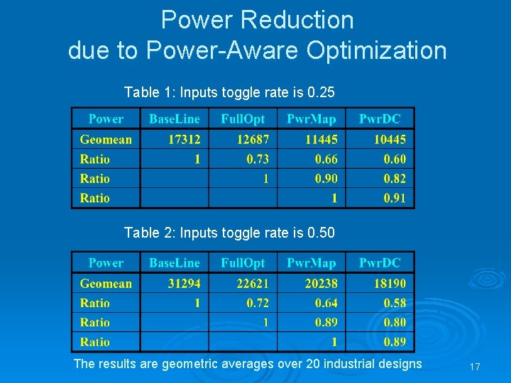
Power Reduction due to Power-Aware Optimization Table 1: Inputs toggle rate is 0. 25 Table 2: Inputs toggle rate is 0. 50 The results are geometric averages over 20 industrial designs 17
Changes in Wire Ratios due to Power-Aware Optimization Wire group codes: T 5: “hot wires” (p > 0. 4) … T 1: “cold wires” (p < 0. 1) 18 where p is the probability of switching (note that p can be more than 0. 5)
Power Dissipation per Wire Group With / Without Power-Aware Optimization Wire (Wire 2) are wires before (after) synthesis. Pwr (Pwr 2) are power dissipations before (after) synthesis. 19
Conclusions Ø Presented several contributions l l l Ø Sim. Switch: Estimation of switching activity Power. Map: An extension of the priority cut LUT mapper [ICCAD’ 07] to prioritize cuts based on switching activity of the nodes Power. DC: An extension of SAT-based resynthesis [FPGA’ 09] to remove signals with high switching Demonstrated reductions in switching activity (without degradation of area and delay) l l 27% reduction due to seq synthesis [ICCAD’ 08] and Wire. Map [FPGA’ 08] against a plain-vanilla flow +19% reduction due to Power. Map and Wire. DC described in this paper 20
Future Work Ø Speeding up switching activity estimation l Ø More accurate power estimation l Ø Estimating glitching in addition to switching Making other transforms power-aware l l Ø Current implementation can be made faster Computing power-aware choices Specialized logic structuring (power gating) Sequential techniques for power reduction l Clock-gating that uses induction to compute signals that are valid clock gates on the reachable states 21

Abstract Ø The paper describes several complementary algorithms for poweraware logic optimization: (1) Sim. Switch is an efficient sequential simulator for estimating switching activity of signals in large sequential designs. (2) Power. Map uses switching activity to make better decisions during power-aware technology mapping. (3) Power. DC is a resynthesis algorithm that eliminates wires with high switching activity. The proposed simulator draws on new ideas in logic representation and is geared for speed, e. g. it can simulate a 1 M-node sequential design using 1000 bit patterns for 100 cycles in about 10 seconds on a typical one-core CPU. Experiments show that, although each technique contributes to the final quality, it is their combination that gives the best results. When applied to industrial designs in a highly-optimized industrial flow, previous work on sequential synthesis nd wire-aware technology mapping led to a 27. 6% reduction in switching activity, while the techniques of this paper reduce it additionally by 19. 6% without a substantial increase in runtime or degradation of other metrics. 22
- Slides: 22