POWER OPTIMIZATION OF CMOS PROGRAMMABLE GAIN AMPLIFIERS WITH
POWER OPTIMIZATION OF CMOS PROGRAMMABLE GAIN AMPLIFIERS WITH HIGH DYNAMIC RANGE AND COMMON-MODE FEED-FORWARD CIRCUIT A. J. Ginés*, R. Doldán, A. Rueda and E. Peralías Instituto de Microelectrónica de Sevilla (CNM-CSIC) University of Seville (Spain) IEEE ICECS 2010
Contents § Motivations § State-of-the-Art in Low Voltage PGAs § Close-loop vs. Open-loop Architectures § Proposed PGA Architecture § Design Methodology § Common-Mode Feed-forward Circuit (CMFFC) § Verification: § Post-layout Simulation Results (3 -stage PGA) § Experimental Results (stage core) § Conclusions
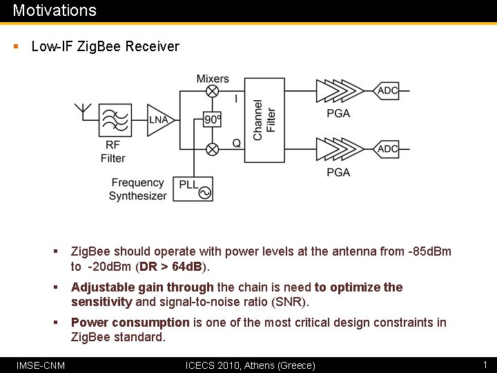
Motivations § Low-IF Zig. Bee Receiver § Zig. Bee should operate with power levels at the antenna from -85 d. Bm to -20 d. Bm (DR > 64 d. B). § Adjustable gain through the chain is need to optimize the sensitivity and signal-to-noise ratio (SNR). § Power consumption is one of the most critical design constraints in Zig. Bee standard. IMSE-CNM ICECS 2010, Athens (Greece) 1
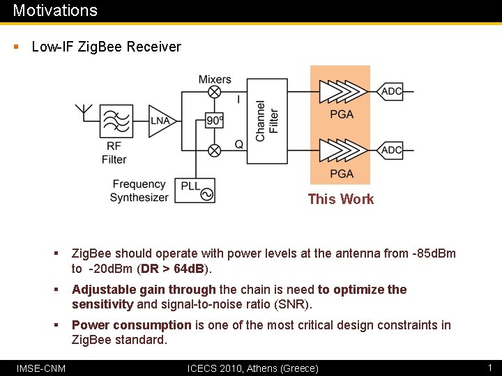
Motivations § Low-IF Zig. Bee Receiver This Work § Zig. Bee should operate with power levels at the antenna from -85 d. Bm to -20 d. Bm (DR > 64 d. B). § Adjustable gain through the chain is need to optimize the sensitivity and signal-to-noise ratio (SNR). § Power consumption is one of the most critical design constraints in Zig. Bee standard. IMSE-CNM ICECS 2010, Athens (Greece) 1
Contents § Motivations § State-of-the-Art in Low Voltage PGAs § Close-loop vs. Open-loop Architectures § Proposed PGA Architecture § Design Methodology § Common-Mode Feed-forward Circuit (CMFFC) § Verification: § Post-layout Simulation Results (3 -stage PGA) § Experimental Results (stage core) § Conclusions
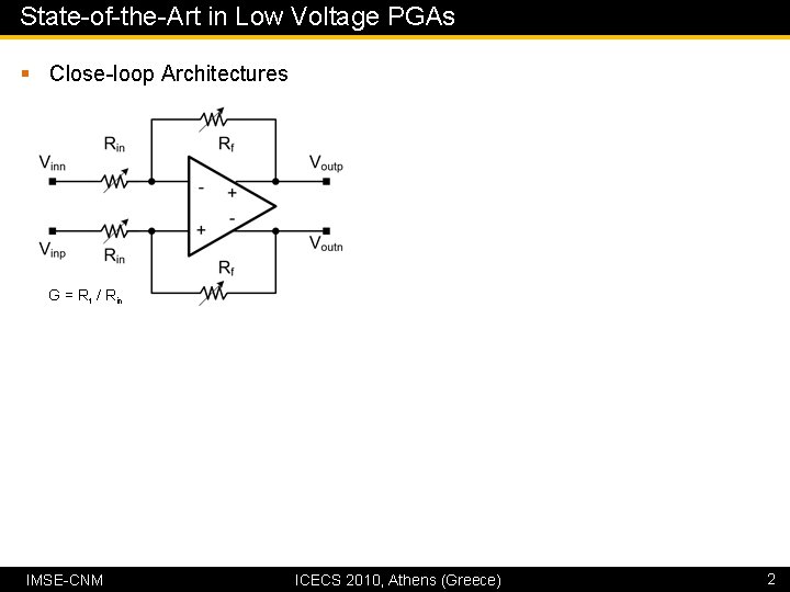
State-of-the-Art in Low Voltage PGAs § Close-loop Architectures G = Rf / Rin IMSE-CNM ICECS 2010, Athens (Greece) 2
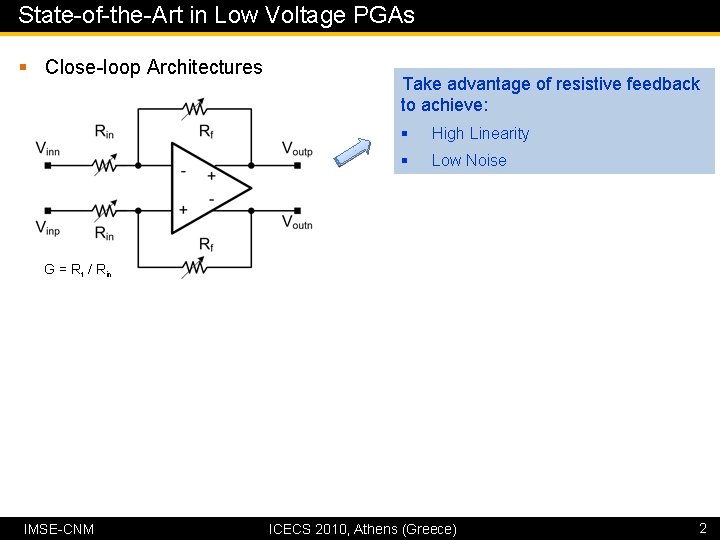
State-of-the-Art in Low Voltage PGAs § Close-loop Architectures Take advantage of resistive feedback to achieve: § High Linearity § Low Noise G = Rf / Rin IMSE-CNM ICECS 2010, Athens (Greece) 2
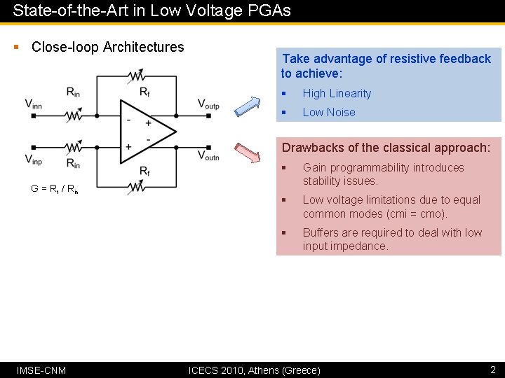
State-of-the-Art in Low Voltage PGAs § Close-loop Architectures Take advantage of resistive feedback to achieve: § High Linearity § Low Noise Drawbacks of the classical approach: G = Rf / Rin IMSE-CNM § Gain programmability introduces stability issues. § Low voltage limitations due to equal common modes (cmi = cmo). § Buffers are required to deal with low input impedance. ICECS 2010, Athens (Greece) 2
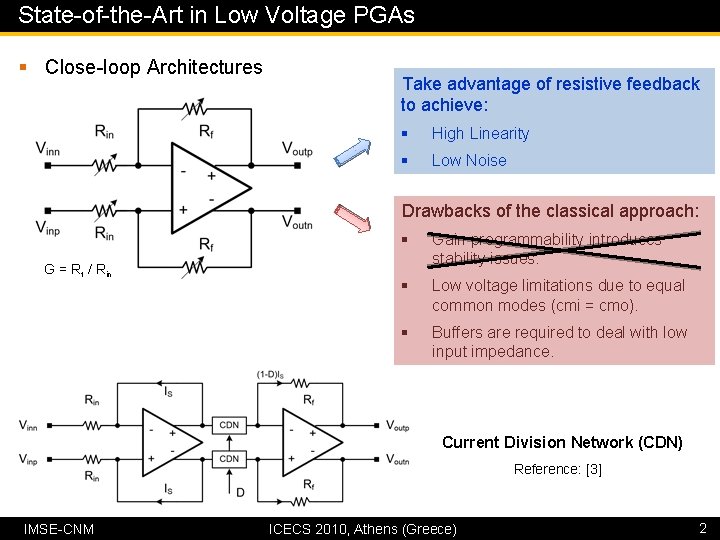
State-of-the-Art in Low Voltage PGAs § Close-loop Architectures Take advantage of resistive feedback to achieve: § High Linearity § Low Noise Drawbacks of the classical approach: G = Rf / Rin § Gain programmability introduces stability issues. § Low voltage limitations due to equal common modes (cmi = cmo). § Buffers are required to deal with low input impedance. Current Division Network (CDN) Reference: [3] IMSE-CNM ICECS 2010, Athens (Greece) 2
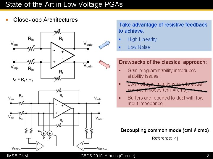
State-of-the-Art in Low Voltage PGAs § Close-loop Architectures Take advantage of resistive feedback to achieve: § High Linearity § Low Noise Drawbacks of the classical approach: G = Rf / Rin § Gain programmability introduces stability issues. § Low voltage limitations due to equal common modes (cmi = cmo). § Buffers are required to deal with low input impedance. Decoupling common mode (cmi ≠ cmo) Reference: [4] IMSE-CNM ICECS 2010, Athens (Greece) 2
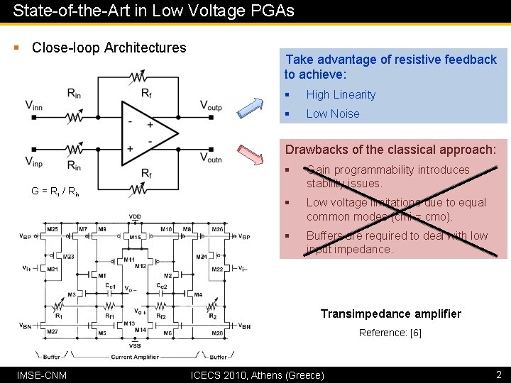
State-of-the-Art in Low Voltage PGAs § Close-loop Architectures Take advantage of resistive feedback to achieve: § High Linearity § Low Noise Drawbacks of the classical approach: G = Rf / Rin § Gain programmability introduces stability issues. § Low voltage limitations due to equal common modes (cmi = cmo). § Buffers are required to deal with low input impedance. Transimpedance amplifier Reference: [6] IMSE-CNM ICECS 2010, Athens (Greece) 2
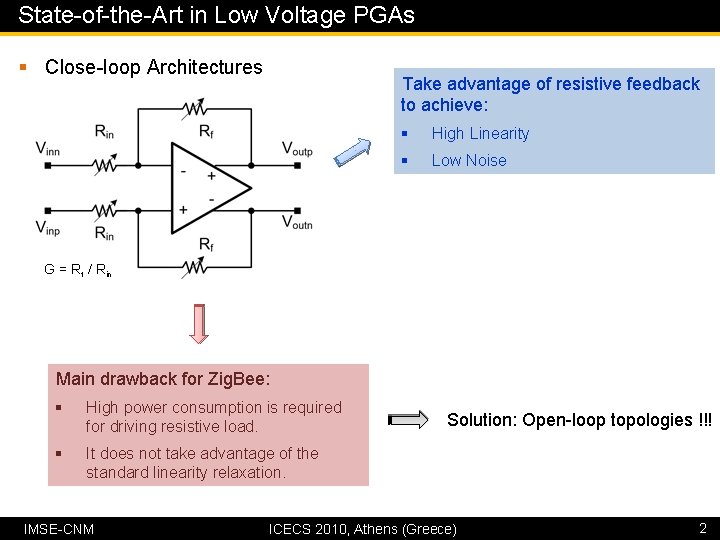
State-of-the-Art in Low Voltage PGAs § Close-loop Architectures Take advantage of resistive feedback to achieve: § High Linearity § Low Noise G = Rf / Rin Main drawback for Zig. Bee: § High power consumption is required for driving resistive load. § It does not take advantage of the standard linearity relaxation. IMSE-CNM Solution: Open-loop topologies !!! ICECS 2010, Athens (Greece) 2
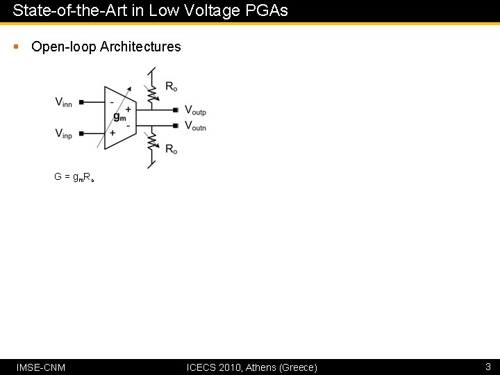
State-of-the-Art in Low Voltage PGAs § Open-loop Architectures G = g m Ro IMSE-CNM ICECS 2010, Athens (Greece) 3
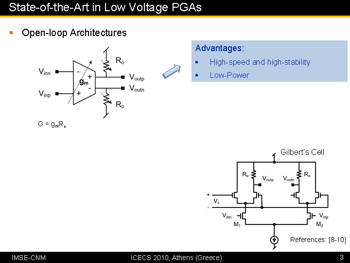
State-of-the-Art in Low Voltage PGAs § Open-loop Architectures Advantages: § High-speed and high-stability § Low-Power G = g m Ro Gilbert’s Cell References: [8 -10] IMSE-CNM ICECS 2010, Athens (Greece) 3
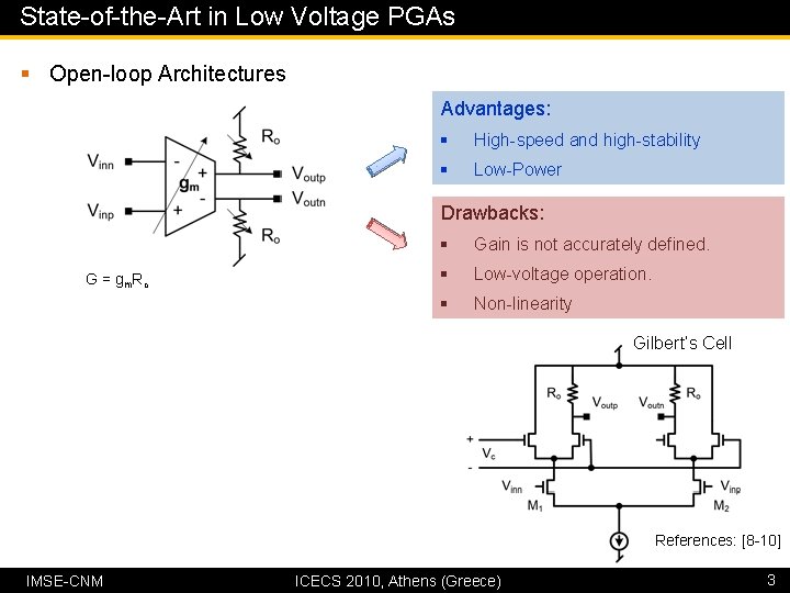
State-of-the-Art in Low Voltage PGAs § Open-loop Architectures Advantages: § High-speed and high-stability § Low-Power Drawbacks: G = g m Ro § Gain is not accurately defined. § Low-voltage operation. § Non-linearity Gilbert’s Cell References: [8 -10] IMSE-CNM ICECS 2010, Athens (Greece) 3
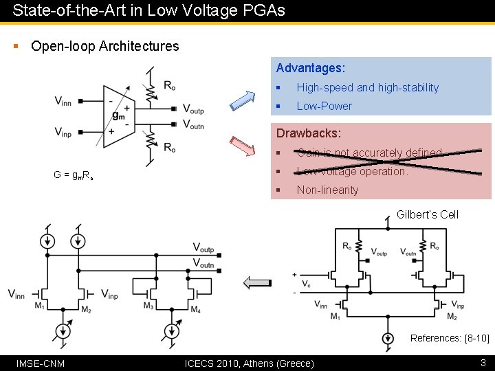
State-of-the-Art in Low Voltage PGAs § Open-loop Architectures Advantages: § High-speed and high-stability § Low-Power Drawbacks: G = g m Ro § Gain is not accurately defined. § Low-voltage operation. § Non-linearity Gilbert’s Cell References: [8 -10] IMSE-CNM ICECS 2010, Athens (Greece) 3
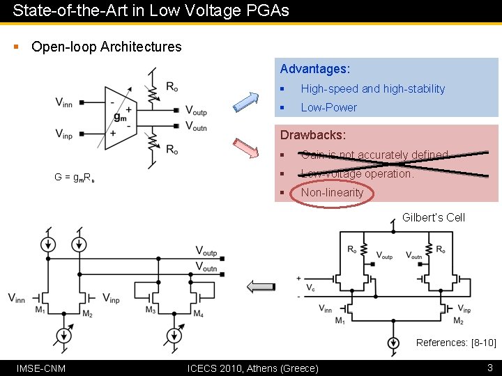
State-of-the-Art in Low Voltage PGAs § Open-loop Architectures Advantages: § High-speed and high-stability § Low-Power Drawbacks: G = g m Ro § Gain is not accurately defined. § Low-voltage operation. § Non-linearity Gilbert’s Cell References: [8 -10] IMSE-CNM ICECS 2010, Athens (Greece) 3
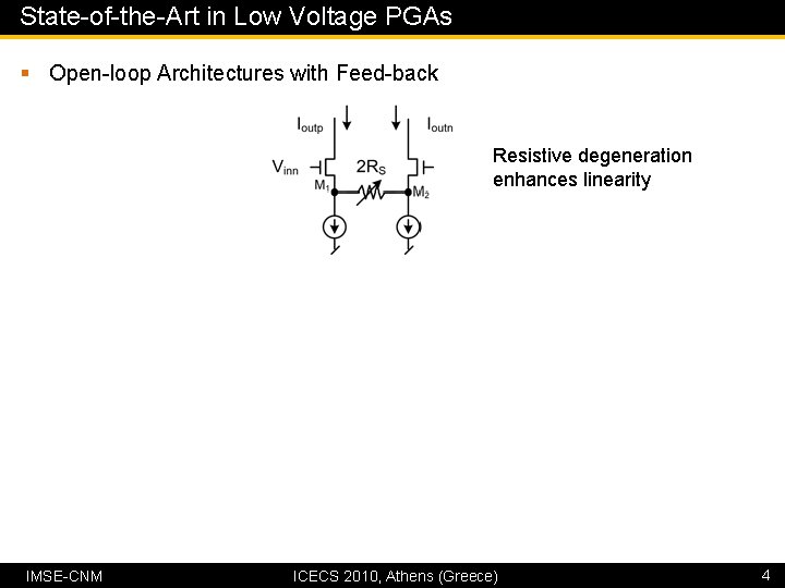
State-of-the-Art in Low Voltage PGAs § Open-loop Architectures with Feed-back Resistive degeneration enhances linearity IMSE-CNM ICECS 2010, Athens (Greece) 4
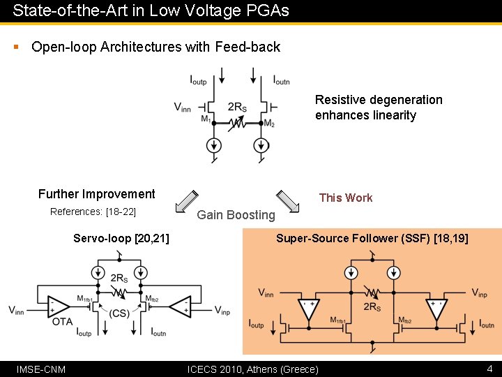
State-of-the-Art in Low Voltage PGAs § Open-loop Architectures with Feed-back Resistive degeneration enhances linearity Further Improvement References: [18 -22] Servo-loop [20, 21] IMSE-CNM This Work Gain Boosting Super-Source Follower (SSF) [18, 19] ICECS 2010, Athens (Greece) 4
Contents § Motivations § State-of-the-Art in Low Voltage PGAs § Close-loop vs. Open-loop Architectures § Proposed PGA Architecture § Design Methodology § Common-Mode Feed-forward Circuit (CMFFC) § Verification: § Post-layout Simulation Results (3 -stage PGA) § Experimental Results (stage core) § Conclusions
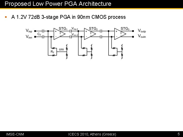
Proposed Low Power PGA Architecture § A 1. 2 V 72 d. B 3 -stage PGA in 90 nm CMOS process IMSE-CNM ICECS 2010, Athens (Greece) 5
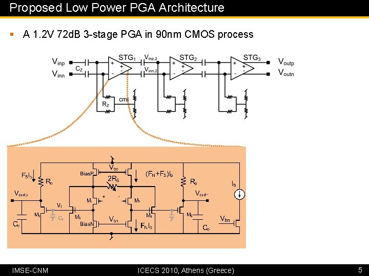
Proposed Low Power PGA Architecture § A 1. 2 V 72 d. B 3 -stage PGA in 90 nm CMOS process IMSE-CNM ICECS 2010, Athens (Greece) 5
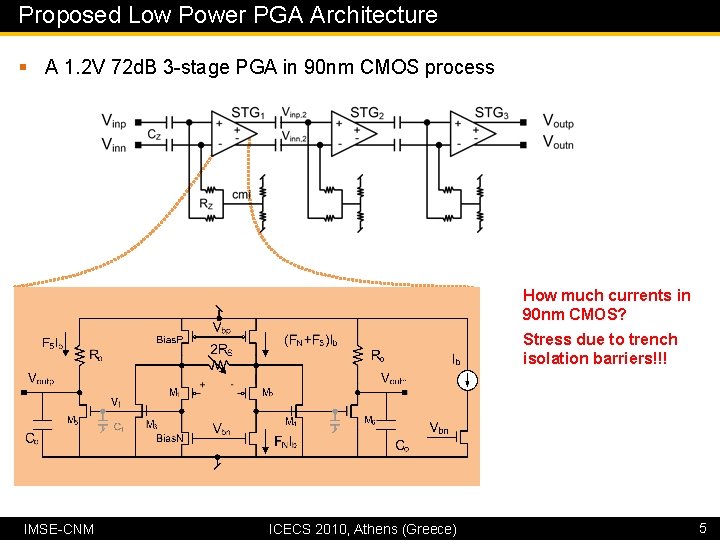
Proposed Low Power PGA Architecture § A 1. 2 V 72 d. B 3 -stage PGA in 90 nm CMOS process How much currents in 90 nm CMOS? Stress due to trench isolation barriers!!! IMSE-CNM ICECS 2010, Athens (Greece) 5
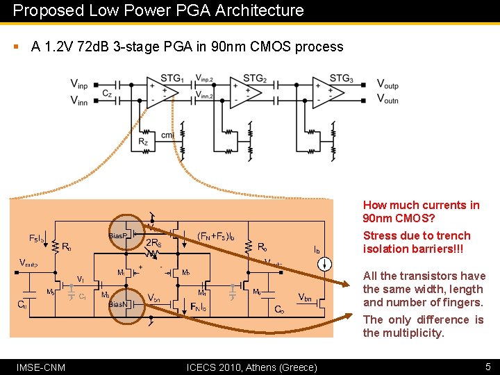
Proposed Low Power PGA Architecture § A 1. 2 V 72 d. B 3 -stage PGA in 90 nm CMOS process How much currents in 90 nm CMOS? Stress due to trench isolation barriers!!! All the transistors have the same width, length and number of fingers. The only difference is the multiplicity. IMSE-CNM ICECS 2010, Athens (Greece) 5
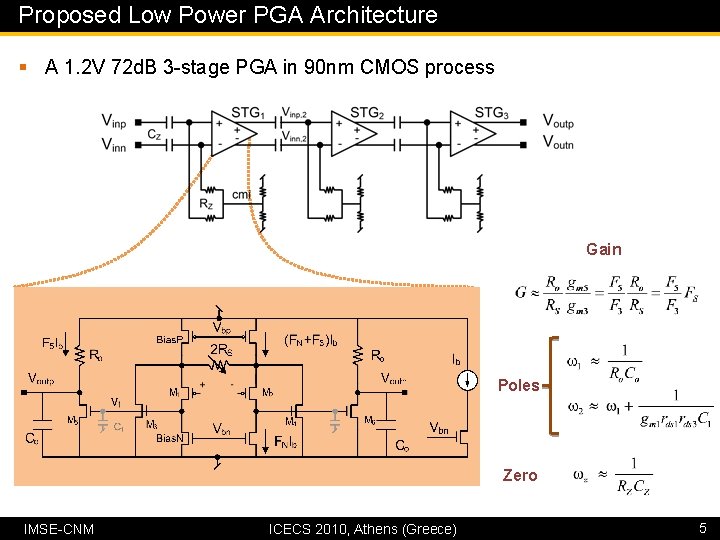
Proposed Low Power PGA Architecture § A 1. 2 V 72 d. B 3 -stage PGA in 90 nm CMOS process Gain Poles Zero IMSE-CNM ICECS 2010, Athens (Greece) 5
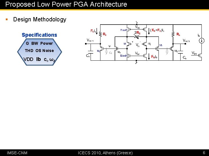
Proposed Low Power PGA Architecture § Design Methodology Specifications G BW Power THD OS Noise VDD Ib C 0 ω2 IMSE-CNM ICECS 2010, Athens (Greece) 6
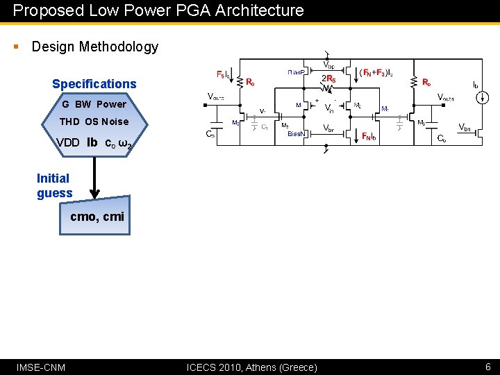
Proposed Low Power PGA Architecture § Design Methodology Specifications G BW Power THD OS Noise VDD Ib C 0 ω2 Initial guess cmo, cmi IMSE-CNM ICECS 2010, Athens (Greece) 6
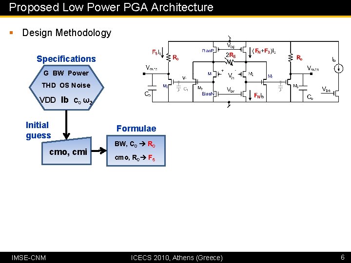
Proposed Low Power PGA Architecture § Design Methodology Specifications G BW Power THD OS Noise VDD Ib C 0 ω2 Initial guess cmo, cmi IMSE-CNM Formulae BW, C 0 R 0 cmo, R 0 F 5 ICECS 2010, Athens (Greece) 6
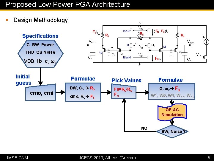
Proposed Low Power PGA Architecture § Design Methodology Specifications G BW Power THD OS Noise VDD Ib C 0 ω2 Initial guess cmo, cmi Formulae BW, C 0 R 0 cmo, R 0 F 5 Pick Values Formulae G, ω2 F 3 Fs=R 0/RS FN W 1, W 5, W 4, WBP, WBN OP-AC Simulation NO IMSE-CNM ICECS 2010, Athens (Greece) BW, Noise ? 6
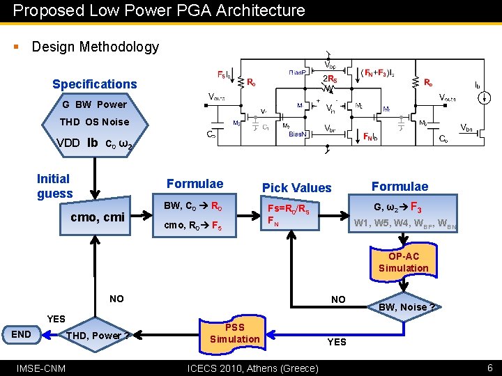
Proposed Low Power PGA Architecture § Design Methodology Specifications G BW Power THD OS Noise VDD Ib C 0 ω2 Initial guess Formulae cmo, cmi BW, C 0 R 0 cmo, R 0 F 5 Pick Values Formulae G, ω2 F 3 Fs=R 0/RS FN W 1, W 5, W 4, WBP, WBN OP-AC Simulation NO YES END IMSE-CNM THD, Power ? NO PSS Simulation ICECS 2010, Athens (Greece) BW, Noise ? YES 6
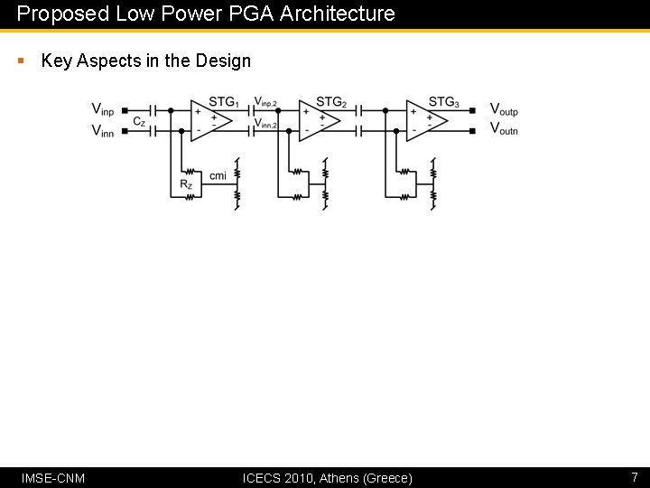
Proposed Low Power PGA Architecture § Key Aspects in the Design IMSE-CNM ICECS 2010, Athens (Greece) 7
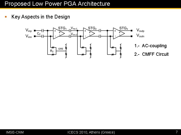
Proposed Low Power PGA Architecture § Key Aspects in the Design 1. - AC-coupling 2. - CMFF Circuit IMSE-CNM ICECS 2010, Athens (Greece) 7
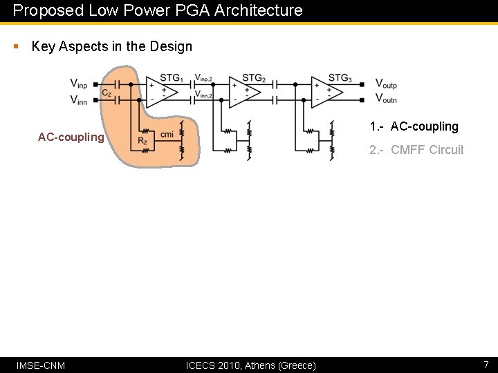
Proposed Low Power PGA Architecture § Key Aspects in the Design 1. - AC-coupling IMSE-CNM 2. - CMFF Circuit ICECS 2010, Athens (Greece) 7
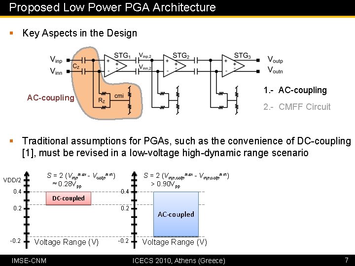
Proposed Low Power PGA Architecture § Key Aspects in the Design 1. - AC-coupling 2. - CMFF Circuit § Traditional assumptions for PGAs, such as the convenience of DC-coupling [1], must be revised in a low-voltage high-dynamic range scenario S = 2 (Vinpmax - Voutpmin) ≈ 0. 28 Vpp VDD/2 0. 4 DC-coupled 0. 2 -0. 2 0. 4 0. 2 Voltage Range (V) IMSE-CNM -0. 2 S = 2 (Vinp, outpmax - Vinp, outpmin) > 0. 90 Vpp AC-coupled Voltage Range (V) ICECS 2010, Athens (Greece) 7
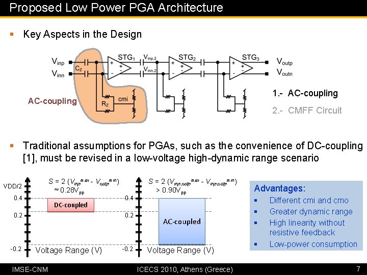
Proposed Low Power PGA Architecture § Key Aspects in the Design 1. - AC-coupling 2. - CMFF Circuit § Traditional assumptions for PGAs, such as the convenience of DC-coupling [1], must be revised in a low-voltage high-dynamic range scenario S = 2 (Vinpmax - Voutpmin) ≈ 0. 28 Vpp VDD/2 0. 4 DC-coupled 0. 2 -0. 2 0. 4 0. 2 Voltage Range (V) IMSE-CNM -0. 2 S = 2 (Vinp, outpmax - Vinp, outpmin) > 0. 90 Vpp AC-coupled Voltage Range (V) ICECS 2010, Athens (Greece) Advantages: § § Different cmi and cmo Greater dynamic range High linearity without resistive feedback Low-power consumption 7
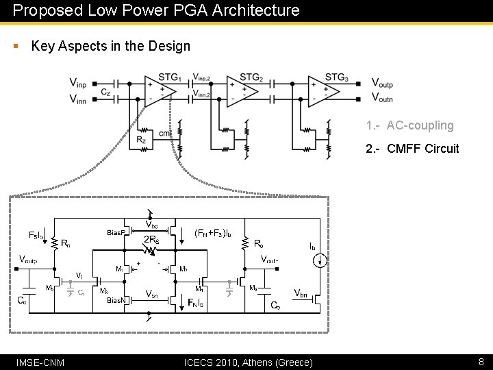
Proposed Low Power PGA Architecture § Key Aspects in the Design 1. - AC-coupling 2. - CMFF Circuit IMSE-CNM ICECS 2010, Athens (Greece) 8
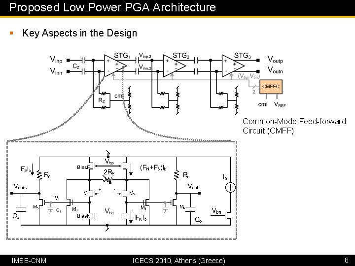
Proposed Low Power PGA Architecture § Key Aspects in the Design Common-Mode Feed-forward Circuit (CMFF) IMSE-CNM ICECS 2010, Athens (Greece) 8
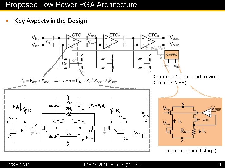
Proposed Low Power PGA Architecture § Key Aspects in the Design Common-Mode Feed-forward Circuit (CMFF) ( common for all stage) IMSE-CNM ICECS 2010, Athens (Greece) 8
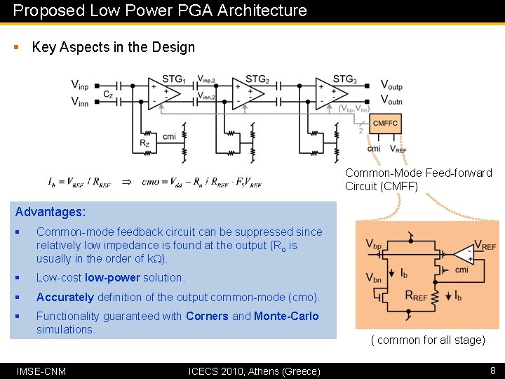
Proposed Low Power PGA Architecture § Key Aspects in the Design Common-Mode Feed-forward Circuit (CMFF) Advantages: § Common-mode feedback circuit can be suppressed since relatively low impedance is found at the output (Ro is usually in the order of k ). § Low-cost low-power solution. § Accurately definition of the output common-mode (cmo). § Functionality guaranteed with Corners and Monte-Carlo simulations. IMSE-CNM ICECS 2010, Athens (Greece) ( common for all stage) 8
Contents § Motivations § State-of-the-Art in Low Voltage PGAs § Close-loop vs. Open-loop Architectures § Proposed PGA Architecture § Design Methodology § Common-Mode Feed-forward Circuit (CMFFC) § Verification: § Post-layout Simulation Results (3 -stage PGA) § Experimental Results (stage core) § Conclusions
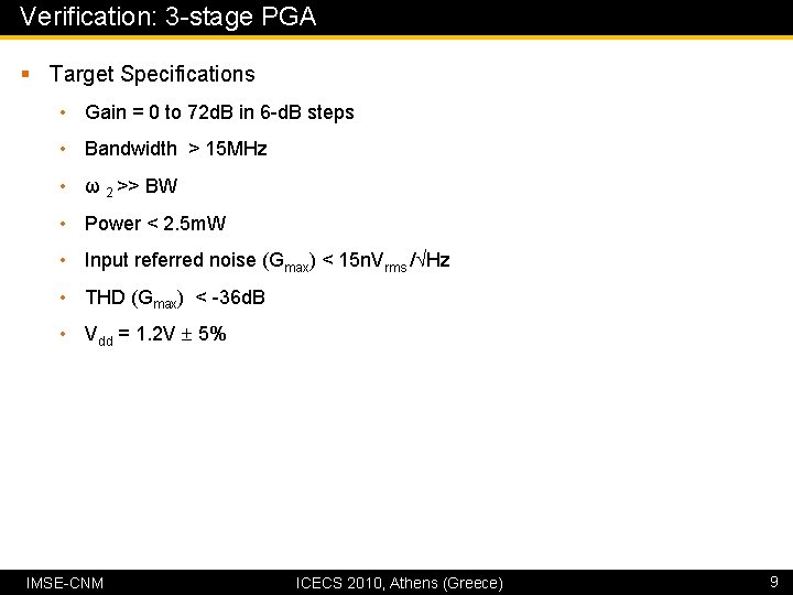
Verification: 3 -stage PGA § Target Specifications • Gain = 0 to 72 d. B in 6 -d. B steps • Bandwidth > 15 MHz • ω 2 >> BW • Power < 2. 5 m. W • Input referred noise (Gmax) < 15 n. Vrms / Hz • THD (Gmax) < -36 d. B • Vdd = 1. 2 V 5% IMSE-CNM ICECS 2010, Athens (Greece) 9
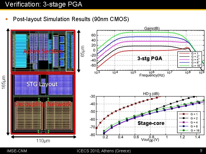
Verification: 3 -stage PGA 165µm Active Section 65µm § Post-layout Simulation Results (90 nm CMOS) 3 -stg PGA STG Layout Decoupling Network Stage-core 110µm IMSE-CNM ICECS 2010, Athens (Greece) 9
Verification: 3 -stage PGA § Corners and Monte-Carlo Specifications (Post-layout) IMSE-CNM ICECS 2010, Athens (Greece) 10
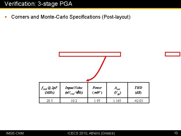
Verification: 3 -stage PGA § Corners and Monte-Carlo Specifications (Post-layout) IMSE-CNM f 3 d. B @ 2 p. F (MHz) Input Noise (n. Vrms / Hz) Power ( m. W ) Aout (Vpp) THD (d. B) 20. 5 10. 2 1. 95 1. 165 -42. 03 ICECS 2010, Athens (Greece) 10
Verification: 3 -stage PGA § Corners and Monte-Carlo Specifications (Post-layout) IMSE-CNM ICECS 2010, Athens (Greece) 10
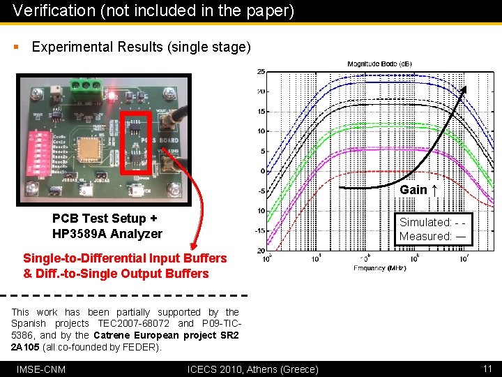
Verification (not included in the paper) § Experimental Results (single stage) Gain ↑ PCB Test Setup + HP 3589 A Analyzer Simulated: - Measured: ― Single-to-Differential Input Buffers & Diff. -to-Single Output Buffers This work has been partially supported by the Spanish projects TEC 2007 -68072 and P 09 -TIC 5386, and by the Catrene European project SR 2 2 A 105 (all co-founded by FEDER). IMSE-CNM ICECS 2010, Athens (Greece) 11
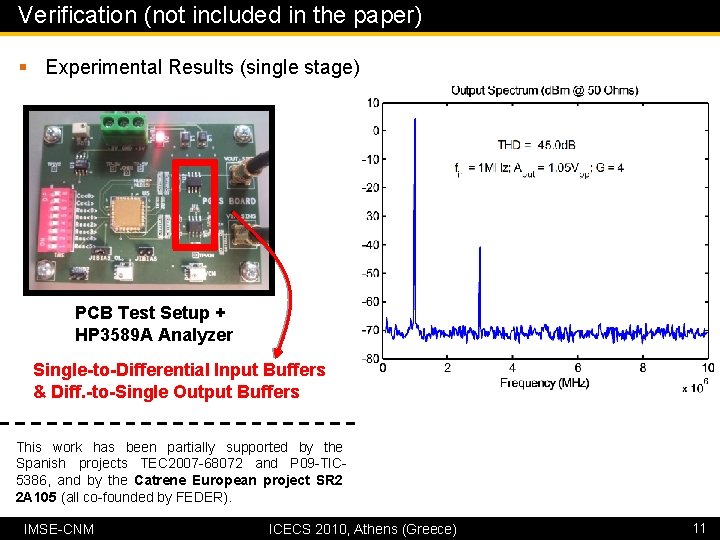
Verification (not included in the paper) § Experimental Results (single stage) PCB Test Setup + HP 3589 A Analyzer Single-to-Differential Input Buffers & Diff. -to-Single Output Buffers This work has been partially supported by the Spanish projects TEC 2007 -68072 and P 09 -TIC 5386, and by the Catrene European project SR 2 2 A 105 (all co-founded by FEDER). IMSE-CNM ICECS 2010, Athens (Greece) 11
Contents § Motivations § State-of-the-Art in Low Voltage PGAs § Close-loop vs. Open-loop Architectures § Proposed PGA Architecture § Design Methodology § Common-Mode Feed-forward Circuit (CMFFC) § Verification: § Post-layout Simulation Results (3 -stage PGA) § Experimental Results (stage core) § Conclusions
Conclusions § In this paper, we have shown that open-loop topologies with gain boosting present an optimum trade-off between power consumption and linearity for Zig. Bee applications. § We have proposed a design methodology for low-voltage PGAs with resistive degeneration. § The developed design flow is shown with a 1. 2 V 72 d. B 1. 95 m. W PGA implementation in a TSMC 90 nm CMOS process. § Power optimization is improved thanks to the use of a front-end capacitive decoupling network and a common-mode feed-forward circuit shared between all stages. § The front-end capacitive decoupling network also improves the PGA dynamic range. Actually, a THD < -42 d. B is achieved for a 1. 2 Vpp output excursion, G = {4, 8, 16}. IMSE-CNM ICECS 2010, Athens (Greece) 12
POWER OPTIMIZATION OF CMOS PROGRAMMABLE GAIN AMPLIFIERS WITH HIGH DYNAMIC RANGE AND COMMON-MODE FEED-FORWARD CIRCUIT Thank you very much for your attendance Questions? A. J. Ginés, Email: gines@imse-cnm. csic. es Instituto de Microelectrónica de Sevilla (CNM-CSIC) University of Seville (Spain)
- Slides: 50