Power Integrity for HighSpeed Design on MultiLayer PCBs

Power Integrity for High-Speed Design on Multi-Layer PCBs Concepts and Physics James L. Drewniak Clear Signal Solutions and Missouri S&T EMC Laboratory james. drewniak@clearsig. com CEMC IAB Meeting May 8 -10, 2012 University/Center Confidential
Contributors ● ● ● IBM – B. Archambeault, S. Connor, M. Cocchini, W. Becker, M. Cracraft, A. Ruehli Cisco – B. Achkir, S. Scearce, Q. Gaumer, M. Sapazhnikov Missouri S&T – B. Zhao, S. Bai, S. Liang, X. Zhu, K. Shringapure, S. Pan, J. Xu, J. Fan CEMC IAB Meeting May 8 -10, 2012 University/Center Confidential 2
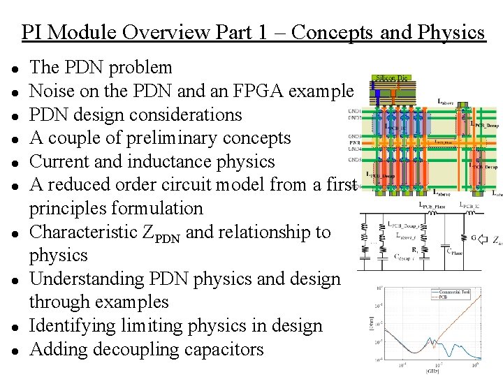
PI Module Overview Part 1 – Concepts and Physics ● ● ● ● ● The PDN problem Noise on the PDN and an FPGA example PDN design considerations A couple of preliminary concepts Current and inductance physics A reduced order circuit model from a first principles formulation Characteristic ZPDN and relationship to physics Understanding PDN physics and design through examples Identifying limiting physics in design Adding decoupling capacitors PI - 3
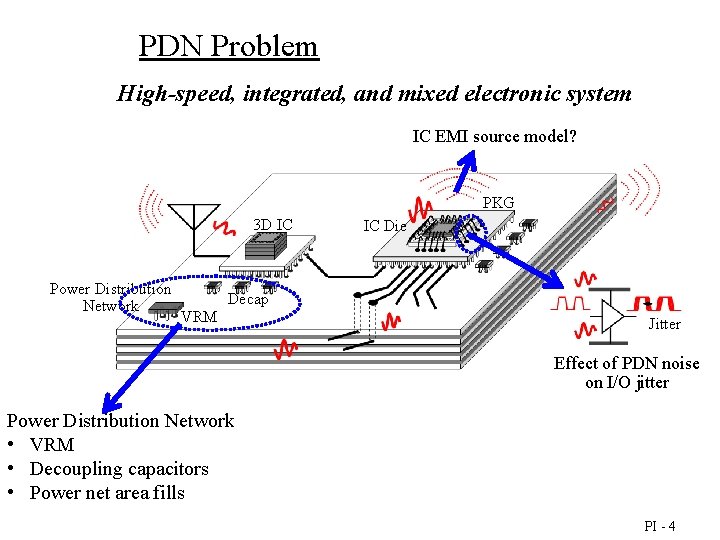
PDN Problem High-speed, integrated, and mixed electronic system IC EMI source model? PKG 3 D IC Power Distribution Network IC Die Decap VRM Jitter Effect of PDN noise on I/O jitter Power Distribution Network • VRM • Decoupling capacitors • Power net area fills PI - 4
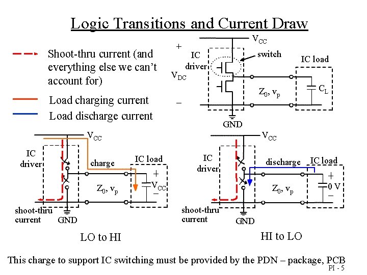
Logic Transitions and Current Draw VCC Shoot-thru current (and everything else we can’t account for) switch IC driver VDC Z 0, vp Load charging current Load discharge current charge Z 0, vp VCC IC load IC driver LO to HI discharge VCC Z 0, vp shoot-thru current GND CL GND VCC IC driver IC load 0 V GND HI to LO This charge to support IC switching must be provided by the PDN – package, PCB PI - 5
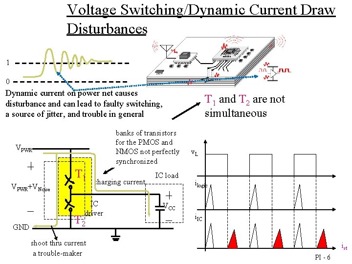
Voltage Switching/Dynamic Current Draw Disturbances 1 0 Dynamic current on power net causes disturbance and can lead to faulty switching, a source of jitter, and trouble in general banks of transistors for the PMOS and NMOS not perfectly synchronized VPWR T 1 VPWR+VNoise GND T 1 and T 2 are not simultaneous charging current IC driver T 2 shoot thru current a trouble-maker IC load v. L ilogic VCC i. IC ist PI - 6
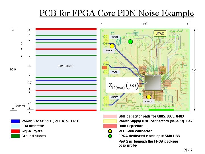
PCB for FPGA Core PDN Noise Example Port 1 Port 2 Power planes: VCC, VCCN, VCCPD FR 4 dielectric Signal layers Ground planes SMT capacitor pads for 0805, 0603, 0403 Power Supply BNC connectors (sensing line) Bulk Capacitor VCC SMA connector FPGA dedicated clock input SMA U 33 Port 2 is beneath the FPGA package coax probe PI - 7
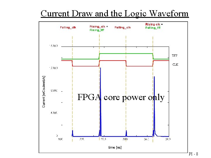
Current Draw and the Logic Waveform FPGA core power only PI - 8
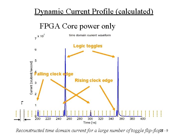
Dynamic Current Profile (calculated) FPGA Core power only Logic toggles Falling clock edge Rising clock edge PI - 9 Reconstructed time domain current for a large number of toggle flip-flops
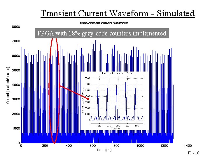
Transient Current Waveform - Simulated FPGA with 18% grey-code counters implemented PI - 10
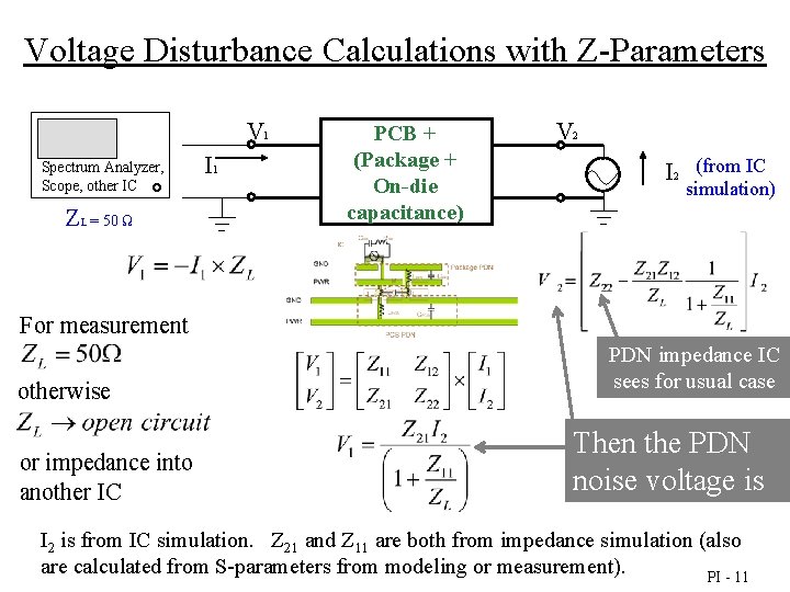
Voltage Disturbance Calculations with Z-Parameters V 1 Spectrum Analyzer, Scope, other IC ZL = 50 Ω I 1 PCB + (Package + On-die capacitance) V 2 I 2 (from IC simulation) For measurement otherwise or impedance into another IC PDN impedance IC sees for usual case Then the PDN noise voltage is I 2 is from IC simulation. Z 21 and Z 11 are both from impedance simulation (also are calculated from S-parameters from modeling or measurement). PI - 11
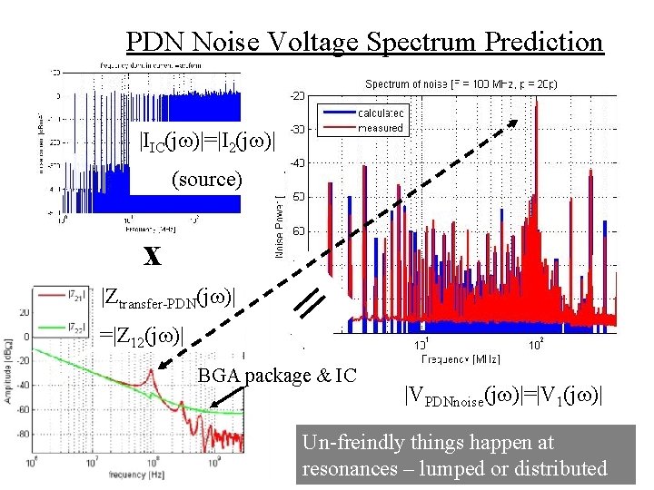
PDN Noise Voltage Spectrum Prediction |IIC(jw)|=|I 2(jw)| (source) x |Ztransfer-PDN(jw)| =|Z 12(jw)| = BGA package & IC |VPDNnoise(jw)|=|V 1(jw)| Un-freindly things happen at resonances – lumped or distributed PI - 12
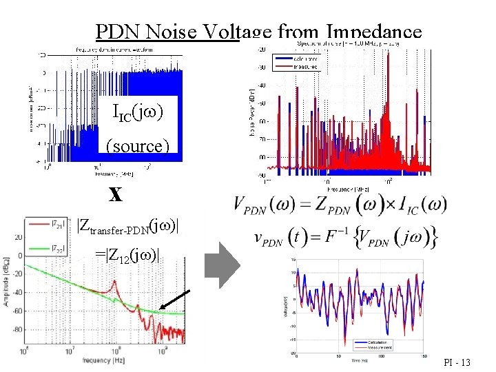
PDN Noise Voltage from Impedance IIC(jw) (source) x |Ztransfer-PDN(jw)| =|Z 12(jw)| PI - 13
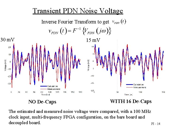
Transient PDN Noise Voltage Inverse Fourier Transform to get 30 m. V 15 m. V NO De-Caps WITH 16 De-Caps The estimated and measured noise voltage were compared, with a 100 MHz clock input, multi-frequency FPGA configuration, on the bare board and decoupled board. PI - 14
PI Module Overview Part 1 – Concepts and Physics ● ● ● ● ● The PDN problem Noise on the PDN and an FPGA example PDN design considerations A couple of preliminary concepts Current and inductance physics A reduced order circuit model from a first principles formulation Characteristic ZPDN and relationship to physics Understanding PDN physics and design through examples Identifying limiting physics in design Adding decoupling capacitors PI - 15
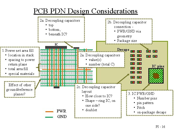
PCB PDN Design Considerations 2 a. Decoupling capacitors • top • bottom, • beneath IC? 2 b. Decoupling capacitor connection • PWR/GND via geometry • Package size IC Decaps 2 a. Decoupling capacitors • value(s) • number (total C) 1. Power net area fill • location in stack • spacing to power return plane • total area fill • special materials Effect of other ground/reference planes? PWR GND 2 c. Decoupling capacitor layout • How close to IC? • Shape – ring IC, on one side? • doublet IC pins 3. IC PWR/GND • Number pins • pin pattern • Pitch • on-package decaps PI - 16
PI Module Overview Part 1 – Concepts and Physics ● ● The PDN problem Noise on the PDN and an FPGA example PDN design considerations A couple of preliminary concepts – – Responses for RLC circuits High-frequency current path PI - 17
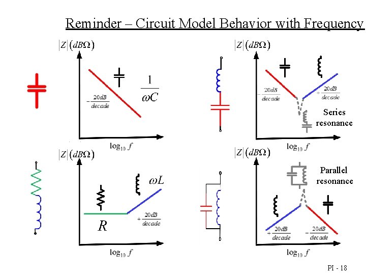
Reminder – Circuit Model Behavior with Frequency Series resonance Parallel resonance PI - 18
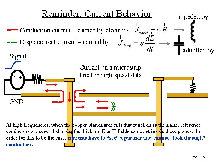
Reminder: Current Behavior impeded by Conduction current – carried by electrons Displacement current – carried by admitted by Signal - + Current on a microstrip line for high-speed data GND At high frequencies, when the copper planes/area fills that function as the signal reference conductors are several skin depths thick, no E or H fields can exist inside these planes. In order for this to be the case, currents have to “see” a partner and cannot “look through” conductors. PI - 19
PI Module Overview Part 1 – Concepts and Physics ● ● ● The PDN problem Noise on the PDN and an FPGA example PDN design considerations A couple of preliminary concepts Current and inductance physics – – – Conduction current path through layers (vertical) on PCB PDN and associated inductance Decomposing the inductance into pieces Current path across the power net area fill and the ground power return current PI - 20
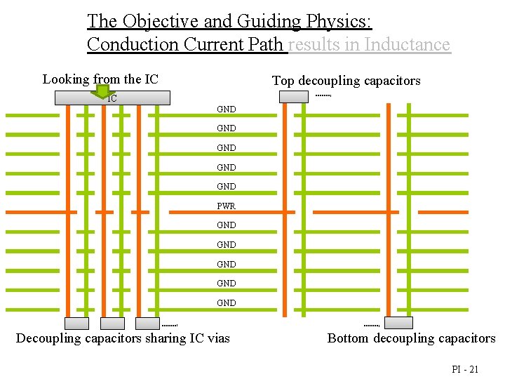
The Objective and Guiding Physics: Conduction Current Path results in Inductance Looking from the IC IC Top decoupling capacitors IC GND GND GND PWR GND GND GND Decoupling capacitors sharing IC vias Bottom decoupling capacitors PI - 21
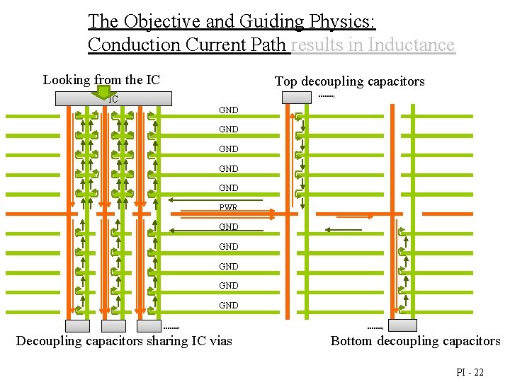
The Objective and Guiding Physics: Conduction Current Path results in Inductance Looking from the IC IC Top decoupling capacitors IC GND GND GND PWR GND GND GND Decoupling capacitors sharing IC vias Bottom decoupling capacitors PI - 22
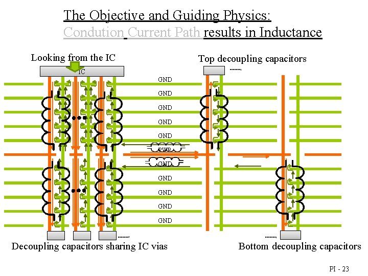
The Objective and Guiding Physics: Condution Current Path results in Inductance Looking from the IC IC Top decoupling capacitors IC GND GND GND PWR GND GND GND Decoupling capacitors sharing IC vias Bottom decoupling capacitors PI - 23
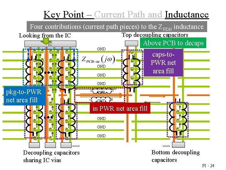
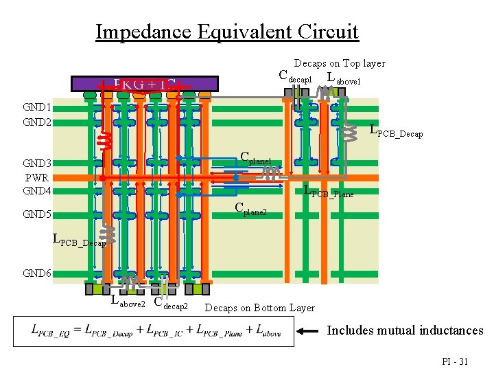
Key Point – Current Path and Inductance Four contributions (current path pieces) to the ZPDN inductance Looking from the IC IC Top decoupling capacitors IC Above PCB to decaps GND GND caps-to. PWR net area fill GND pkg-to-PWR net area fill PWR GND in. GND PWR net area fill GND GND Decoupling capacitors sharing IC vias Bottom decoupling capacitors PI - 24
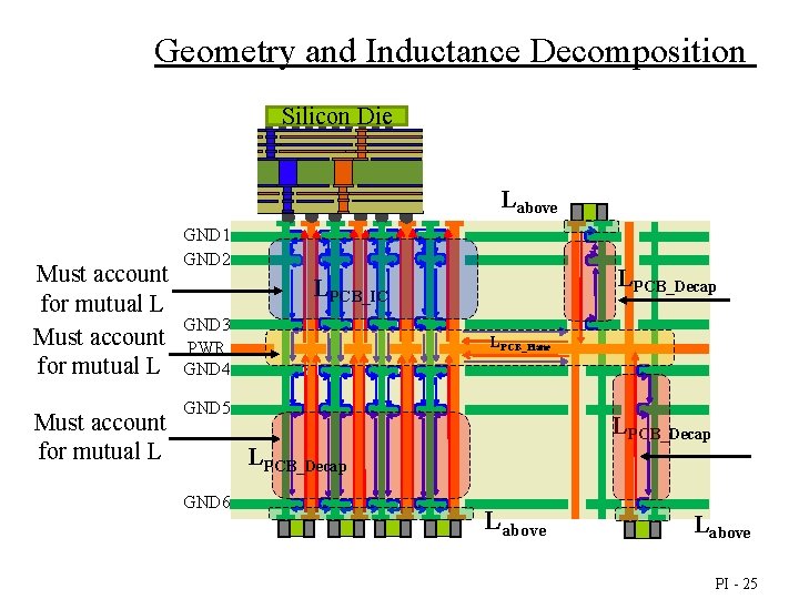
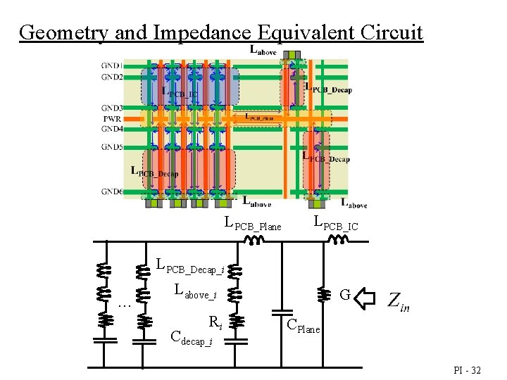
Geometry and Inductance Decomposition Silicon Die Labove Must account for mutual L GND 1 GND 2 LPCB_Decap LPCB_IC GND 3 PWR GND 4 LPCB_Plane GND 5 LPCB_Decap GND 6 Labove PI - 25
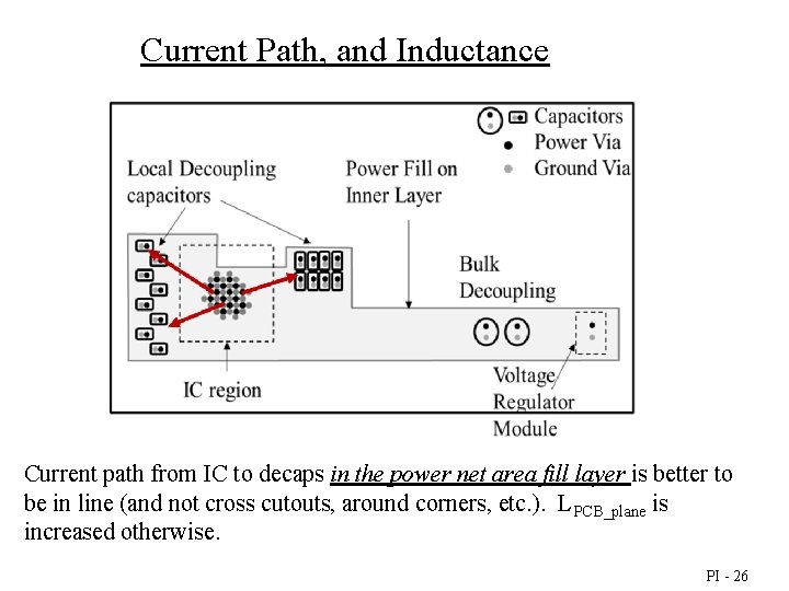
Current Path, and Inductance Current path from IC to decaps in the power net area fill layer is better to be in line (and not cross cutouts, around corners, etc. ). LPCB_plane is increased otherwise. PI - 26
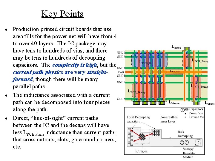
Key Points ● ● ● Production printed circuit boards that use area fills for the power net will have from 4 to over 40 layers. The IC package may have tens to hundreds of vias, and there may be tens to hundreds of decoupling capacitors. The complexity is high, but the current path physics are very straightforward, though there will be many parallel paths. The inductance associated with a current path can be decomposed into four pieces along the path. Direct, “line-of-sight” current paths between the IC and the decaps will have less LPCB Plane inductance than current paths that cross cutouts, slots, go around corners, etc. PI - 27
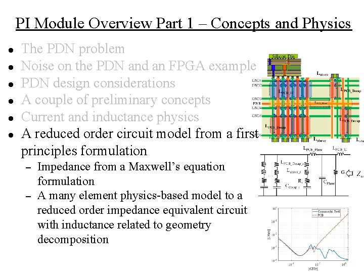
PI Module Overview Part 1 – Concepts and Physics ● ● ● The PDN problem Noise on the PDN and an FPGA example PDN design considerations A couple of preliminary concepts Current and inductance physics A reduced order circuit model from a first principles formulation – – Impedance from a Maxwell’s equation formulation A many element physics-based model to a reduced order impedance equivalent circuit with inductance related to geometry decomposition PI - 28
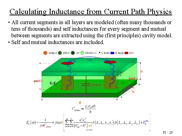
Calculating Inductance from Current Path Physics • All current segments in all layers are modeled (often many thousands or tens of thousands) and self inductances for every segment and mutual between segments are extracted using the (first principles) cavity model. • Self and mutual inductances are included. PI - 29
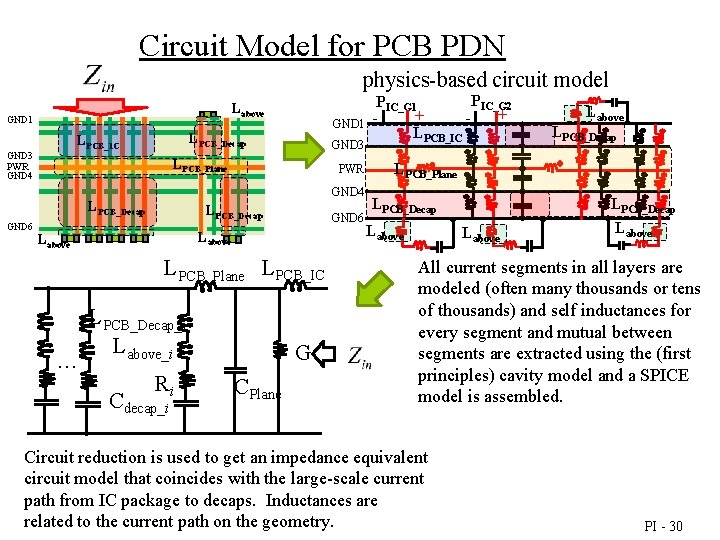
Circuit Model for PCB PDN physics-based circuit model Labove GND 1 LPCB_Decap LPCB_IC GND 3 PWR GND 4 GND 1 GND 3 LPCB_Plane PWR GND 4 LPCB_Decap GND 6 Labove LPCB_Plane LPCB_IC … LPCB_Decap_i Labove_i Ri Cdecap_i G CPlane PIC_G 2 PIC_G 1 + + LPCB_IC Labove LPCB_Decap LPCB_Plane LPCB_Decap Labove All current segments in all layers are modeled (often many thousands or tens of thousands) and self inductances for every segment and mutual between segments are extracted using the (first principles) cavity model and a SPICE model is assembled. Circuit reduction is used to get an impedance equivalent circuit model that coincides with the large-scale current path from IC package to decaps. Inductances are related to the current path on the geometry. PI - 30
Impedance Equivalent Circuit Decaps on Top layer Cdecap 1 PKG + IC Labove 1 GND 2 LPCB_Decap Cplane 1 GND 3 PWR GND 4 LPCB_Plane Cplane 2 GND 5 LPCB_Decap GND 6 Labove 2 Cdecap 2 Decaps on Bottom Layer Includes mutual inductances PI - 31
Geometry and Impedance Equivalent Circuit LPCB_Plane LPCB_IC LPCB_Decap_i … Labove_i Ri Cdecap_i G CPlane PI - 32
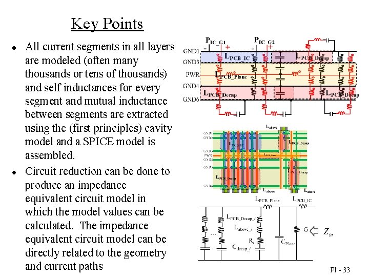
Key Points ● ● All current segments in all layers are modeled (often many thousands or tens of thousands) and self inductances for every segment and mutual inductance between segments are extracted using the (first principles) cavity model and a SPICE model is assembled. Circuit reduction can be done to produce an impedance equivalent circuit model in which the model values can be calculated. The impedance equivalent circuit model can be directly related to the geometry and current paths PI - 33
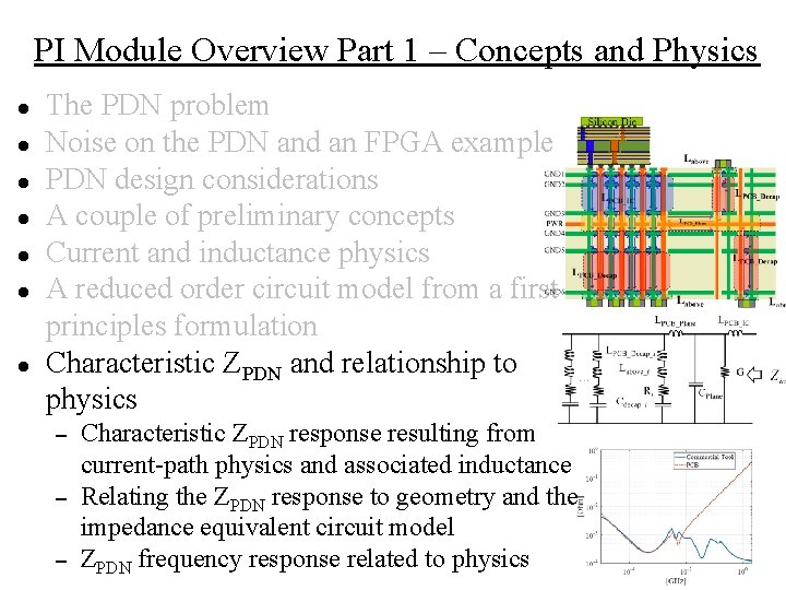
PI Module Overview Part 1 – Concepts and Physics ● ● ● ● The PDN problem Noise on the PDN and an FPGA example PDN design considerations A couple of preliminary concepts Current and inductance physics A reduced order circuit model from a first principles formulation Characteristic ZPDN and relationship to physics – – – Characteristic ZPDN response resulting from current-path physics and associated inductance Relating the ZPDN response to geometry and the impedance equivalent circuit model ZPDN frequency response related to physics PI - 34
![Input Impedance at an IC port [Ω] Resulting ZPDN Response 100 measurement Eq. circuit Input Impedance at an IC port [Ω] Resulting ZPDN Response 100 measurement Eq. circuit](http://slidetodoc.com/presentation_image_h2/3c3fed304bf3c89e8b0ba4e73c50ef9f/image-35.jpg)
Input Impedance at an IC port [Ω] Resulting ZPDN Response 100 measurement Eq. circuit 10 1 Each of these production real PCBs use only a single layer for the power net area fill (with adjacent layers for power return ground). 28 layer PCB 0. 1 6 layer PCB 0. 01 0. 001 0. 1 1 10 1000 Frequency [MHz] 18 layer PCB 44 layer PCB bulk decaps 0402 decaps under IC VRM PI - 35
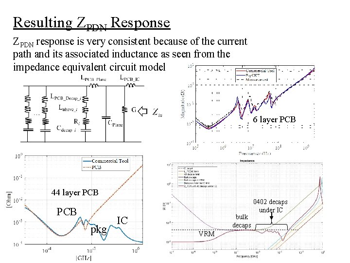
Resulting ZPDN Response ZPDN response is very consistent because of the current path and its associated inductance as seen from the impedance equivalent circuit model 6 layer PCB 44 layer PCB pkg bulk decaps IC 0402 decaps under IC VRM PI - 36
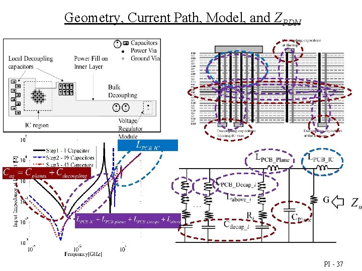
Geometry, Current Path, Model, and ZPDN PI - 37
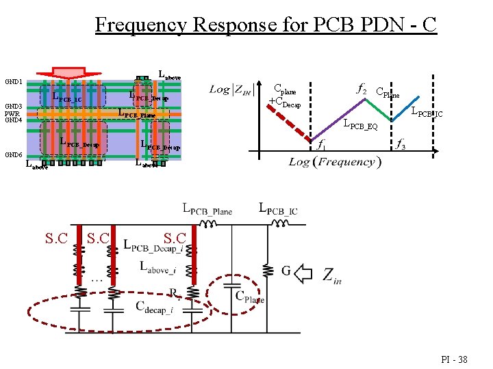
Frequency Response for PCB PDN - C Labove GND 1 LPCB_Decap LPCB_IC GND 3 PWR GND 4 LPCB_Plane LPCB_Decap GND 6 CPlane LPCB_EQ LPCB_IC LPCB_Decap Labove S. C Cplane +CDecap S. C PI - 38
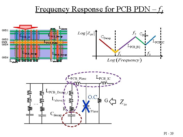
Frequency Response for PCB PDN – f 1 Labove GND 1 LPCB_IC GND 3 PWR GND 4 CDecap LPCB_Plane LPCB_Decap GND 6 LPCB_Decap Labove CPlane LPCB_EQ LPCB_IC LPCB_Decap Labove O. C PI - 39
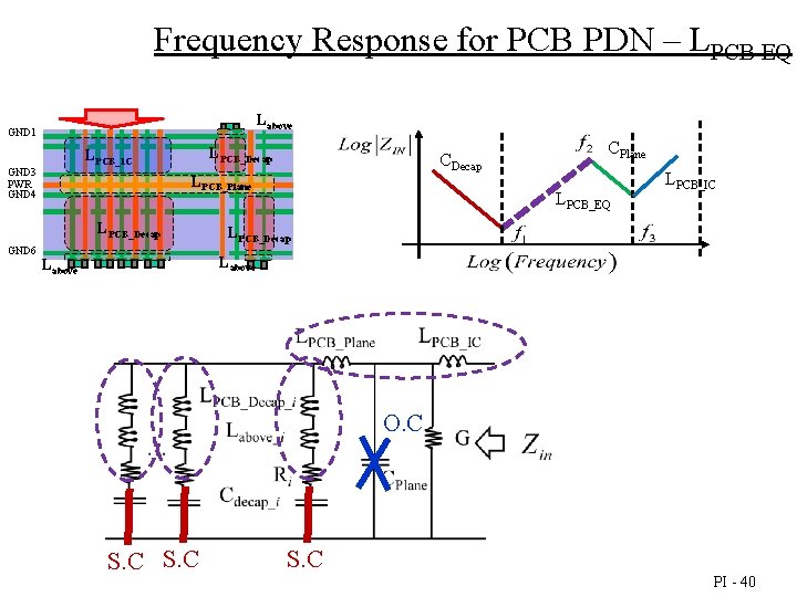
Frequency Response for PCB PDN – LPCB EQ Labove GND 1 LPCB_Decap LPCB_IC GND 3 PWR GND 4 LPCB_Plane LPCB_Decap GND 6 CDecap CPlane LPCB_EQ LPCB_IC LPCB_Decap Labove O. C S. C PI - 40
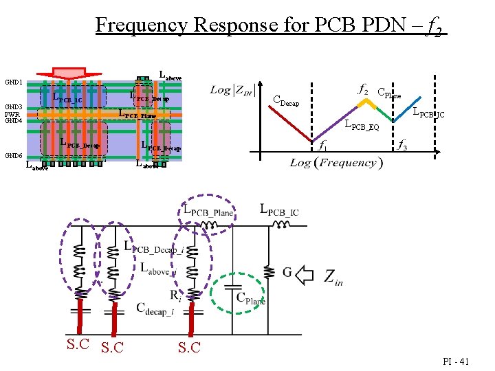
Frequency Response for PCB PDN – f 2 Labove GND 1 LPCB_Decap LPCB_IC GND 3 PWR GND 4 LPCB_Plane LPCB_Decap GND 6 CDecap CPlane LPCB_EQ LPCB_IC LPCB_Decap Labove S. C PI - 41
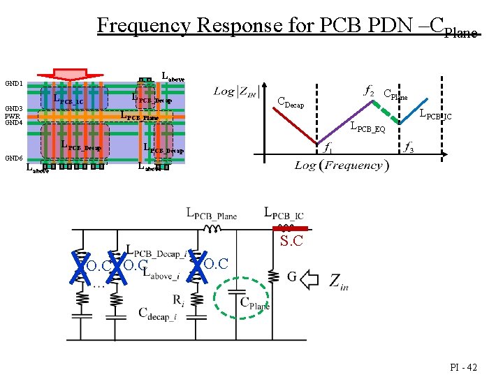
Frequency Response for PCB PDN –CPlane Labove GND 1 LPCB_Decap LPCB_IC GND 3 PWR GND 4 LPCB_Plane LPCB_Decap GND 6 CDecap Labove CPlane LPCB_EQ LPCB_IC LPCB_Decap Labove S. C O. C PI - 42
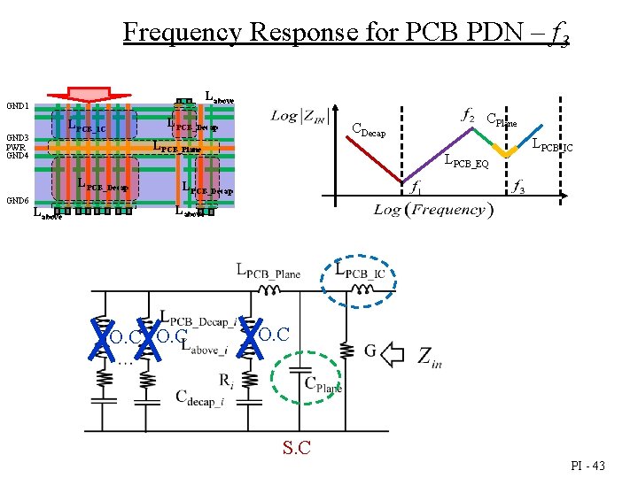
Frequency Response for PCB PDN – f 3 Labove GND 1 LPCB_Decap LPCB_IC GND 3 PWR GND 4 LPCB_Plane LPCB_Decap GND 6 CDecap Labove CPlane LPCB_EQ LPCB_IC LPCB_Decap Labove O. C S. C PI - 43
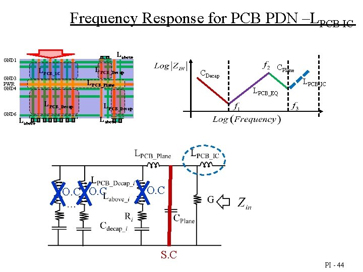
Frequency Response for PCB PDN –LPCB IC Labove GND 1 LPCB_Decap LPCB_IC GND 3 PWR GND 4 LPCB_Plane LPCB_Decap GND 6 CDecap Labove CPlane LPCB_EQ LPCB_IC LPCB_Decap Labove O. C S. C PI - 44
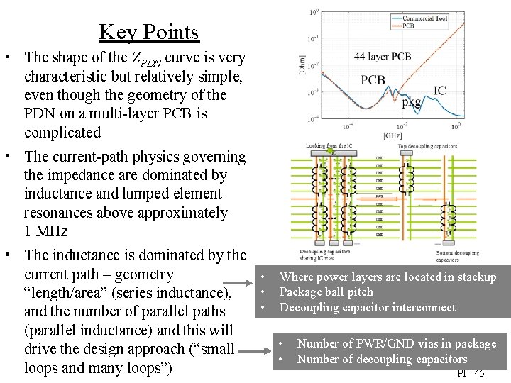
Key Points • The shape of the ZPDN curve is very characteristic but relatively simple, even though the geometry of the PDN on a multi-layer PCB is complicated • The current-path physics governing the impedance are dominated by inductance and lumped element resonances above approximately 1 MHz • The inductance is dominated by the current path – geometry • Where power layers are located in stackup • Package ball pitch “length/area” (series inductance), • Decoupling capacitor interconnect and the number of parallel paths (parallel inductance) and this will • Number of PWR/GND vias in package drive the design approach (“small • Number of decoupling capacitors loops and many loops”) PI - 45
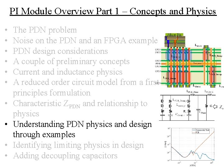
PI Module Overview Part 1 – Concepts and Physics • • • The PDN problem Noise on the PDN and an FPGA example PDN design considerations A couple of preliminary concepts Current and inductance physics A reduced order circuit model from a first principles formulation Characteristic ZPDN and relationship to physics Understanding PDN physics and design through examples Identifying limiting physics in design Adding decoupling capacitors PI - 46
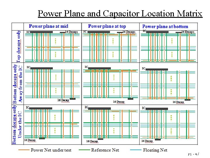
Power Plane and Capacitor Location Matrix PI - 47
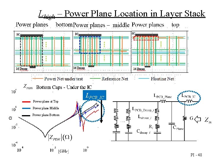
Lhigh – Power Plane Location in Layer Stack Power plane at Top LPCB_IC Power plane Middle Power plane Bottom PI - 48
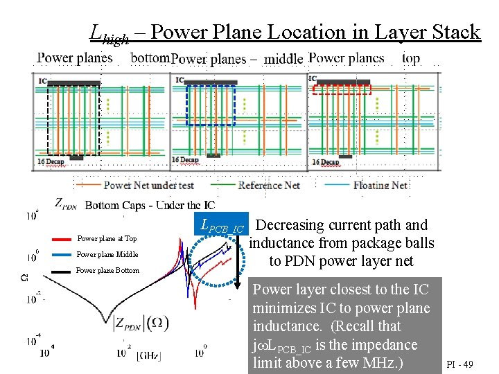
Lhigh – Power Plane Location in Layer Stack Power plane at Top Power plane Middle Power plane Bottom LPCB_IC Decreasing current path and inductance from package balls to PDN power layer net Power layer closest to the IC minimizes IC to power plane inductance. (Recall that jw. LPCB_IC is the impedance limit above a few MHz. ) PI - 49
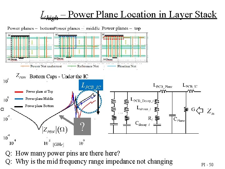
Lhigh – Power Plane Location in Layer Stack Power plane at Top LPCB_IC Power plane Middle Power plane Bottom ? Q: How many power pins are there? Q: Why is the mid frequency range impedance not changing PI - 50
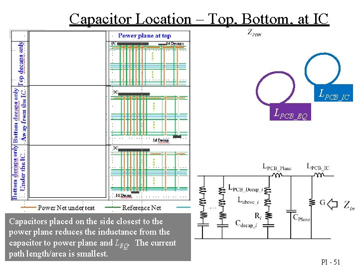
Capacitor Location – Top, Bottom, at IC LPCB_EQ Capacitors placed on the side closest to the power plane reduces the inductance from the capacitor to power plane and LEQ. The current path length/area is smallest. PI - 51
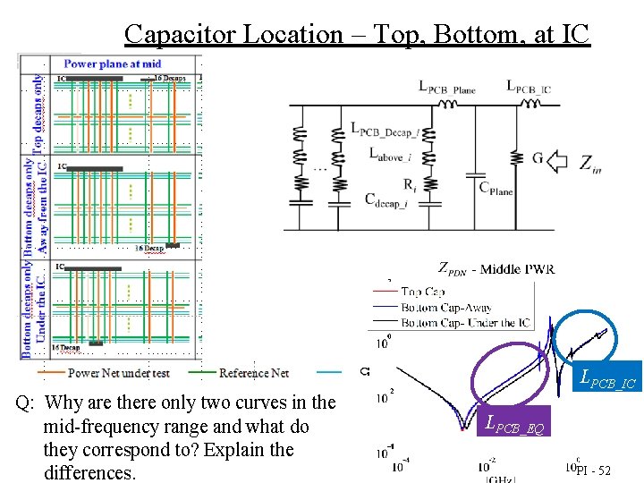
Capacitor Location – Top, Bottom, at IC LPCB_IC Q: Why are there only two curves in the mid-frequency range and what do they correspond to? Explain the differences. LPCB_EQ PI - 52
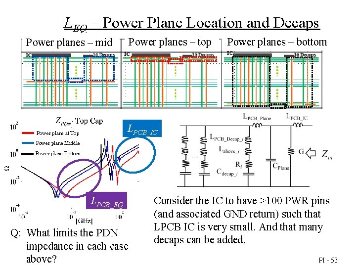
LEQ – Power Plane Location and Decaps Power planes – top Power planes – mid Power planes – bottom LPCB_IC Power plane at Top Power plane Middle Power plane Bottom LPCB_EQ Q: What limits the PDN impedance in each case above? Consider the IC to have >100 PWR pins (and associated GND return) such that LPCB IC is very small. And that many decaps can be added. PI - 53
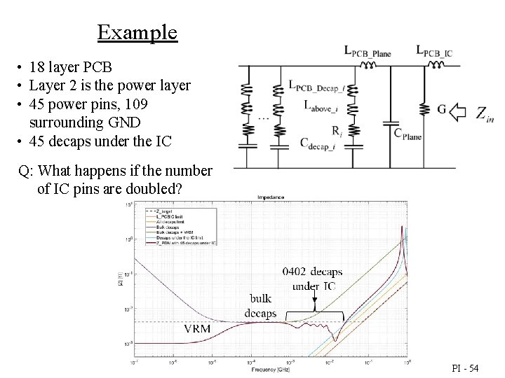
Example • 18 layer PCB • Layer 2 is the power layer • 45 power pins, 109 surrounding GND • 45 decaps under the IC Q: What happens if the number of IC pins are doubled? PI - 54
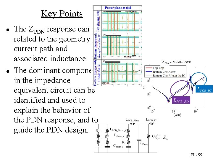
Key Points ● ● The ZPDN response can be related to the geometry, current path and associated inductance. The dominant component in the impedance equivalent circuit can be identified and used to explain the behavior of the PDN response, and to guide the PDN design. PI - 55
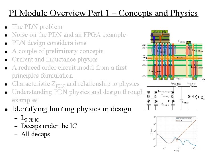
PI Module Overview Part 1 – Concepts and Physics ● ● ● ● ● The PDN problem Noise on the PDN and an FPGA example PDN design considerations A couple of preliminary concepts Current and inductance physics A reduced order circuit model from a first principles formulation Characteristic ZPDN and relationship to physics Understanding PDN physics and design through examples Identifying limiting physics in design – – – LPCB IC Decaps under the IC All decaps PI - 56

LPCB IC Physical Limit LPCB IC is the physical limit at high frequencies when the current returns through the interplane capacitance of the power net area fill and return O. C S. C LPCB IC limit PI - 57
![Input Impedance at an IC port [Ω] Real Board LPCB IC Examples 100 measurement Input Impedance at an IC port [Ω] Real Board LPCB IC Examples 100 measurement](http://slidetodoc.com/presentation_image_h2/3c3fed304bf3c89e8b0ba4e73c50ef9f/image-58.jpg)
Input Impedance at an IC port [Ω] Real Board LPCB IC Examples 100 measurement Eq. circuit 10 1 28 layer PCB 0. 1 6 layer PCB 0. 01 0. 001 0. 1 1 10 1000 Frequency [MHz] 18 layer PCB 44 layer PCB bulk decaps 0402 decaps under IC VRM PI - 58
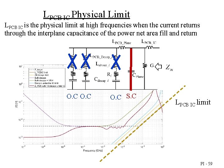
LPCB IC Physical Limit LPCB IC is the physical limit at high frequencies when the current returns through the interplane capacitance of the power net area fill and return O. C S. C LPCB IC limit PI - 59
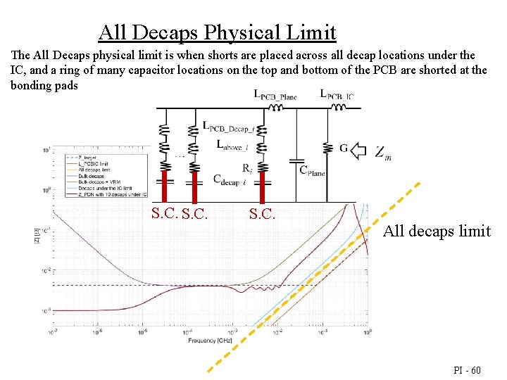
All Decaps Physical Limit The All Decaps physical limit is when shorts are placed across all decap locations under the IC, and a ring of many capacitor locations on the top and bottom of the PCB are shorted at the bonding pads S. C. All decaps limit PI - 60
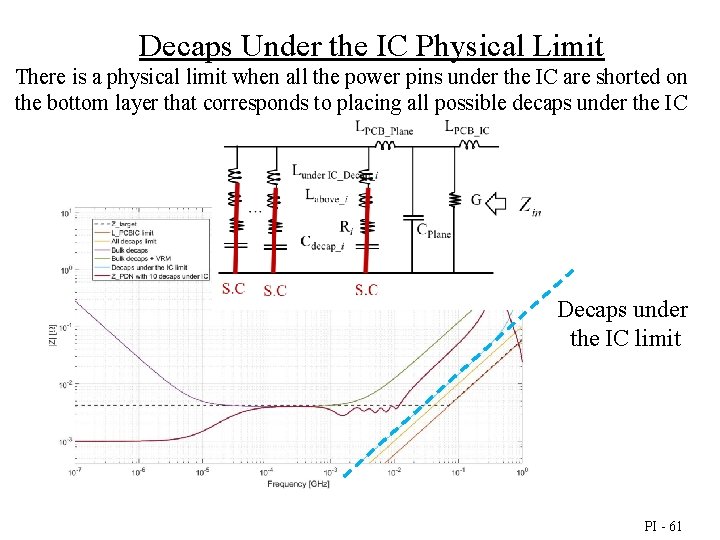
Decaps Under the IC Physical Limit There is a physical limit when all the power pins under the IC are shorted on the bottom layer that corresponds to placing all possible decaps under the IC Decaps under the IC limit PI - 61
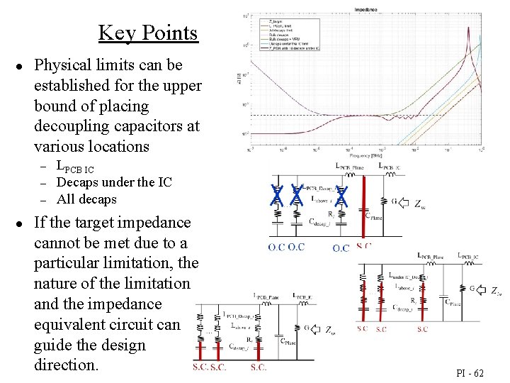
Key Points ● Physical limits can be established for the upper bound of placing decoupling capacitors at various locations – – – ● LPCB IC Decaps under the IC All decaps If the target impedance cannot be met due to a particular limitation, the nature of the limitation and the impedance equivalent circuit can guide the design direction. PI - 62
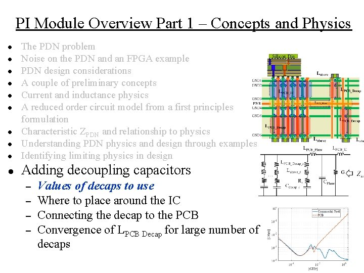
PI Module Overview Part 1 – Concepts and Physics ● The PDN problem Noise on the PDN and an FPGA example PDN design considerations A couple of preliminary concepts Current and inductance physics A reduced order circuit model from a first principles formulation Characteristic ZPDN and relationship to physics Understanding PDN physics and design through examples Identifying limiting physics in design ● Adding decoupling capacitors ● ● ● ● – – Values of decaps to use Where to place around the IC Connecting the decap to the PCB Convergence of LPCB Decap for large number of decaps PI - 63
Two Approaches for SMT Decoupling ● Use an array of capacitor values: – – – ● This may be the best known approach in the signal integrity design community Rationale: to maintain a flat impedance profile below a target impedance over a wide frequency range Typically a logarithmically spaced (10, 22, 47, 100, 220, 470 n. F, etc. ) array of several values per decade. Use a large capacitor value in the package size – – This is less well-known, but an approach in the EMI design community Rationale: to keep impedance as low as possible, less emphasis on a target impedance and a flat profile PI - 64
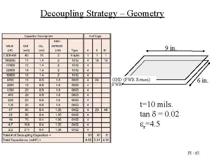
Decoupling Strategy – Geometry 9 in. GND (PWR Return) PWR 6 in. t=10 mils. tan d = 0. 02 er=4. 5 PI - 65
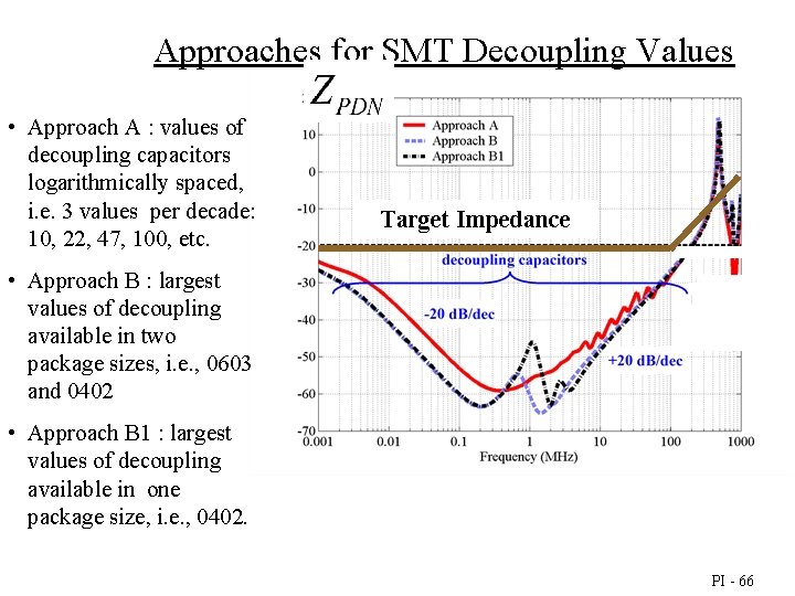
Approaches for SMT Decoupling Values • Approach A : values of decoupling capacitors logarithmically spaced, i. e. 3 values per decade: 10, 22, 47, 100, etc. Target Impedance • Approach B : largest values of decoupling available in two package sizes, i. e. , 0603 and 0402 • Approach B 1 : largest values of decoupling available in one package size, i. e. , 0402. PI - 66
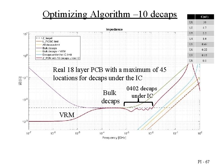
Optimizing Algorithm – 10 decaps Real 18 layer PCB with a maximum of 45 locations for decaps under the IC Bulk decaps 0402 decaps under IC VRM PI - 67
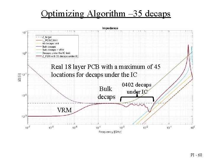
Optimizing Algorithm – 35 decaps Real 18 layer PCB with a maximum of 45 locations for decaps under the IC Bulk decaps 0402 decaps under IC VRM PI - 68
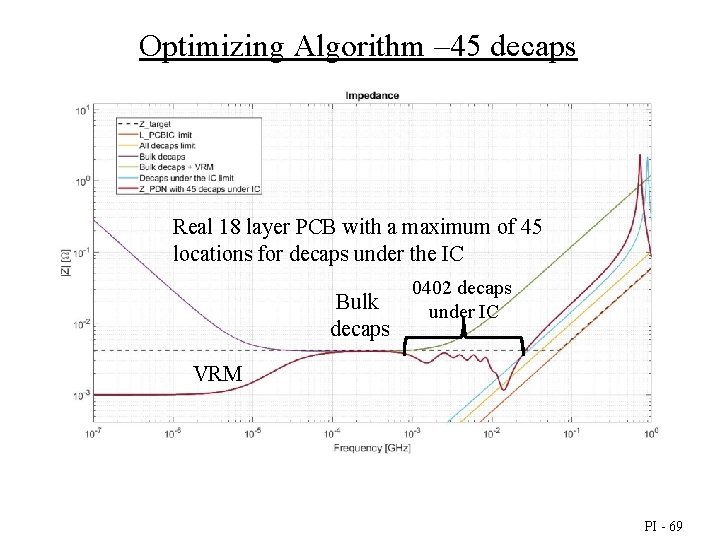
Optimizing Algorithm – 45 decaps Real 18 layer PCB with a maximum of 45 locations for decaps under the IC Bulk decaps 0402 decaps under IC VRM PI - 69
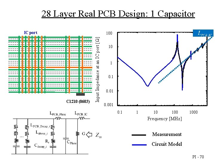
28 Layer Real PCB Design: 1 Capacitor IC port C 1210 (0603) Input Impedance at an IC port [Ω] 100 10 1 0. 01 0. 001 0. 1 1 10 1000 Frequency [MHz] Measurement Circuit Model PI - 70
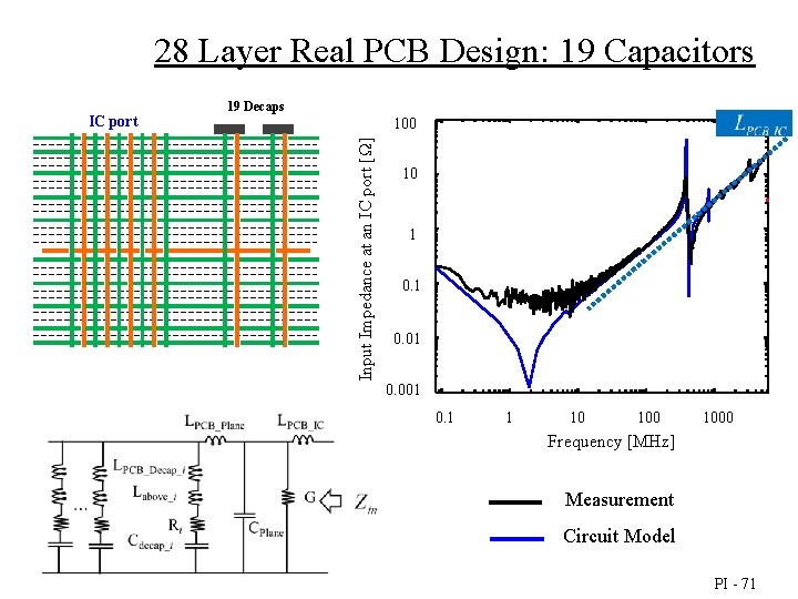
28 Layer Real PCB Design: 19 Capacitors 19 Decaps 100 Input Impedance at an IC port [Ω] IC port 10 1 0. 01 0. 001 0. 1 1 10 1000 Frequency [MHz] Measurement Circuit Model PI - 71
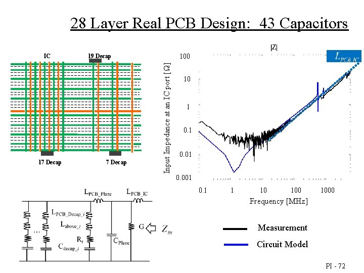
IC 17 Decap 19 Decap 7 Decap Input Impedance at at anan ICIC port [Ω] 28 Layer Real PCB Design: 43 Capacitors 100 10 1 0. 01 0. 001 0. 1 1 10 1000 Frequency [MHz] Measurement Circuit Model PI - 72
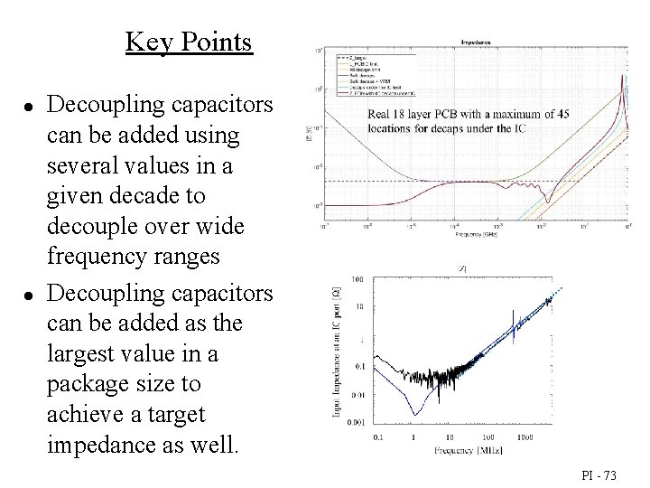
Key Points ● ● Decoupling capacitors can be added using several values in a given decade to decouple over wide frequency ranges Decoupling capacitors can be added as the largest value in a package size to achieve a target impedance as well. PI - 73
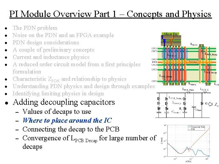
PI Module Overview Part 1 – Concepts and Physics ● The PDN problem Noise on the PDN and an FPGA example PDN design considerations A couple of preliminary concepts Current and inductance physics A reduced order circuit model from a first principles formulation Characteristic ZPDN and relationship to physics Understanding PDN physics and design through examples Identifying limiting physics in design ● Adding decoupling capacitors ● ● ● ● – – Values of decaps to use Where to place around the IC Connecting the decap to the PCB Convergence of LPCB Decap for large number of decaps PI - 74
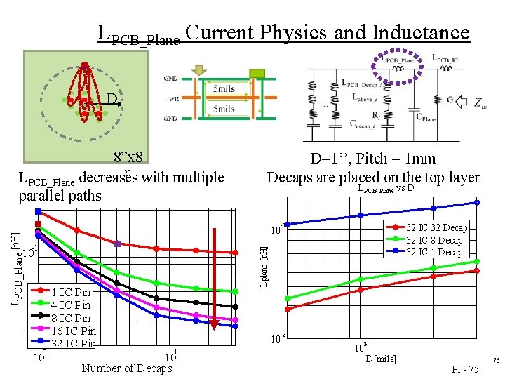
LPCB_Plane Current Physics and Inductance D 8”x 8 ” with multiple LPCB_Plane decreases parallel paths D=1’’, Pitch = 1 mm Decaps are placed on the top layer LPCB_Plane vs D 32 IC 32 Decap 32 IC 8 Decap 32 IC 1 Decap -1 Lplane [n. H] LPCB_Plane [n. H] -1 10 10 1 IC Pin 4 IC Pin 8 IC Pin 16 IC Pin 32 IC Pin -2 10 1 10 Number of Decaps 3 10 D[mils] PI - 75 75
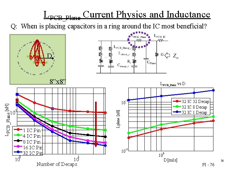
LPCB_Plane Current Physics and Inductance Q: When is placing capacitors in a ring around the IC most beneficial? D 8”x 8” 8”x 8 LPCB_Plane vs D 32 IC 32 Decap 32 IC 8 Decap 32 IC 1 Decap -1 Lplane [n. H] LPCB_Plane [n. H] -1 10 10 1 IC Pin 4 IC Pin 8 IC Pin 16 IC Pin 32 IC Pin -2 10 1 10 Number of Decaps 3 10 D[mils] PI - 76 76
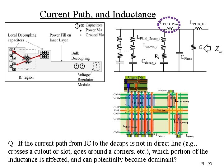
Current Path, and Inductance Q: If the current path from IC to the decaps is not in direct line (e. g. , crosses a cutout or slot, goes around a corners, etc. ), which portion of the inductance is affected, and can potentially become dominant? PI - 77
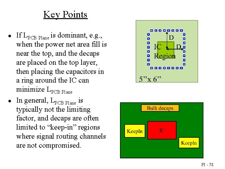
Key Points ● ● If LPCB Plane is dominant, e. g. , when the power net area fill is near the top, and the decaps are placed on the top layer, then placing the capacitors in a ring around the IC can minimize LPCB Plane In general, LPCB Plane is typically not the limiting factor, and decaps are often limited to “keep-in” regions where signal routing channels are not compromised. PI - 78
PI Module Overview Part 1 – Concepts and Physics ● The PDN problem Noise on the PDN and an FPGA example PDN design considerations A couple of preliminary concepts Current and inductance physics A reduced order circuit model from a first principles formulation Characteristic ZPDN and relationship to physics Understanding PDN physics and design through examples Identifying limiting physics in design ● Adding decoupling capacitors ● ● ● ● – – Values of decaps to use Where to place around the IC Connecting the decap to the PCB Convergence of LPCB Decap for large number of decaps PI - 79
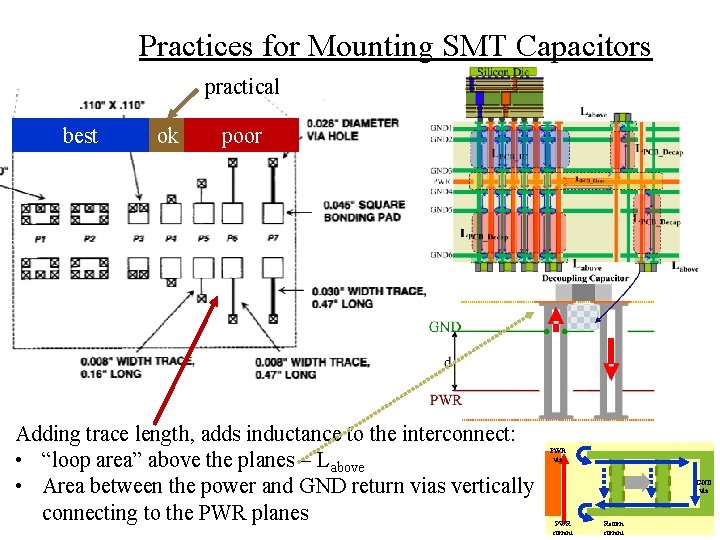
Practices for Mounting SMT Capacitors practical best ok poor Adding trace length, adds inductance to the interconnect: • “loop area” above the planes – Labove • Area between the power and GND return vias vertically connecting to the PWR planes PWR via GND via PWR current Return current PI - 80
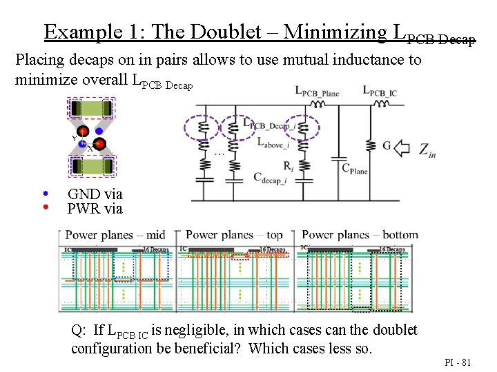
Example 1: The Doublet – Minimizing LPCB Decap Placing decaps on in pairs allows to use mutual inductance to minimize overall LPCB Decap GND via PWR via Q: If LPCB IC is negligible, in which cases can the doublet configuration be beneficial? Which cases less so. PI - 81
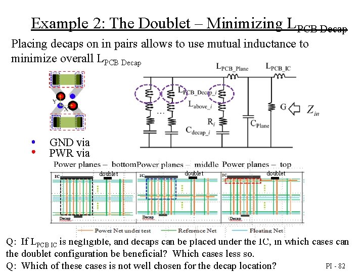
Example 2: The Doublet – Minimizing LPCB Decap Placing decaps on in pairs allows to use mutual inductance to minimize overall LPCB Decap GND via PWR via doublet Q: If LPCB IC is negligible, and decaps can be placed under the IC, in which cases can the doublet configuration be beneficial? Which cases less so. PI - 82 Q: Which of these cases is not well chosen for the decap location?
PI Module Overview Part 1 – Concepts and Physics ● The PDN problem Noise on the PDN and an FPGA example PDN design considerations A couple of preliminary concepts Current and inductance physics A reduced order circuit model from a first principles formulation Characteristic ZPDN and relationship to physics Understanding PDN physics and design through examples Identifying limiting physics in design ● Adding decoupling capacitors ● ● ● ● – – Values of decaps to use Where to place around the IC Connecting the decap to the PCB Convergence of LPCB Decap for large number of decaps PI - 83

LPCB_Decap Convergence Alternating Aligned Doublet D IC D Region 5’’x 6’’ convergence rate for all SMT package sizes *The LPCB_Decap is simulated in PDN Tool and the inductance is extracted from |ZPDN|. PI - 84
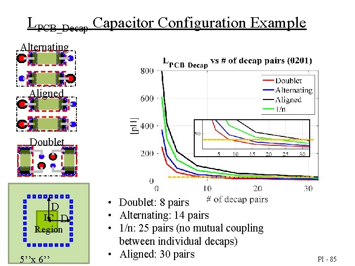
LPCB_Decap Capacitor Configuration Example Alternating Aligned Doublet D IC D Region 5’’x 6’’ • Doublet: 8 pairs • Alternating: 14 pairs • 1/n: 25 pairs (no mutual coupling between individual decaps) • Aligned: 30 pairs PI - 85
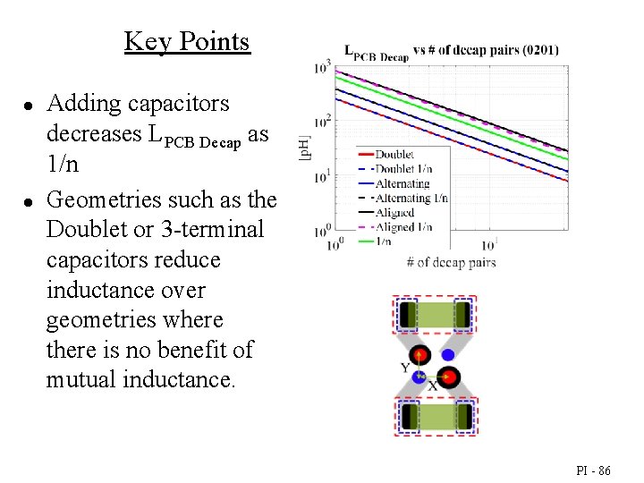
Key Points ● ● Adding capacitors decreases LPCB Decap as 1/n Geometries such as the Doublet or 3 -terminal capacitors reduce inductance over geometries where there is no benefit of mutual inductance. PI - 86
Design Implications ● ● ● Use the impedance equivalent circuit model to try to identify what component is dominant and use it to guide meeting the target impedance. PWR/GND plane pair nearer to the IC in stackup will minimize LPCB_IC from package balls to power net area fill (smaller loop) PWR/GND plane pairs closely spaced will reduce LPCB_plane. Place caps close to the power layer to minimize the inductance from the capacitor to the power net area fill layer, i. e. , LPCB_decaps. (minimize the loop) Placing caps on the underside of PCB opposite package can benefit the design – – ● ● The space is available and requires no additional vias If the pkg/planes/decap path is shorter due to PWR/GND near package in stackup decaps around the IC will be more effective Power and ground vias placed adjacent to the caps reduces the inductance in the current return path (or in the bonding pads). (smaller loops) Capacitor arrangements that utilize mutual inductance, e. g. , doublet, or 3 -terminal capacitor, can significantly reduce LPCB_decaps. PI - 87

Thank you! PI - 88
- Slides: 88