Power FET Structures and Applications Brian Schminski 17
Power FET Structures and Applications Brian Schminski 17 April 2015
Abstract Power FETs are an integral power device, it’s ability to switch from on-state to off-state is crucial in quick switching devices. All the while also having the ability to deal with large current and voltages. Although the Power FET can be tricky when dealing with temperature, has some manufacturing produced devices, but overall it is a necessary to use these FETs.
Outline � � Power FET why is it different? � Structures � FET subtleties � Specific FET example � Applications Why use it? Symbol Fabrication
What makes a Power FET different? Vs Normal FET Vs other power devices � Ability to deal with very high voltages � High commutation Speed � Ability to deal with high sustained currents � Good Efficiency at Low Voltages
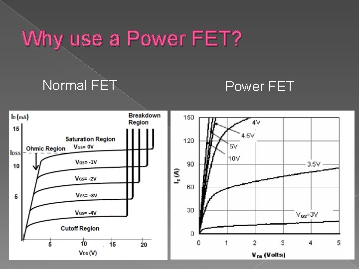
Why use a Power FET? Normal FET Power FET
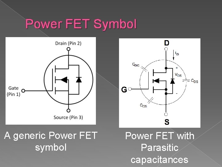
Power FET Symbol A generic Power FET symbol Power FET with Parasitic capacitances
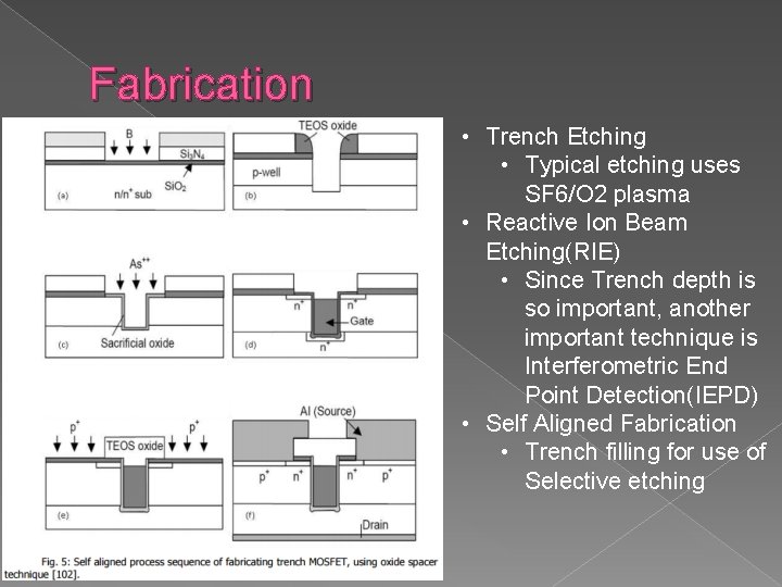
Fabrication • Trench Etching • Typical etching uses SF 6/O 2 plasma • Reactive Ion Beam Etching(RIE) • Since Trench depth is so important, another important technique is Interferometric End Point Detection(IEPD) • Self Aligned Fabrication • Trench filling for use of Selective etching
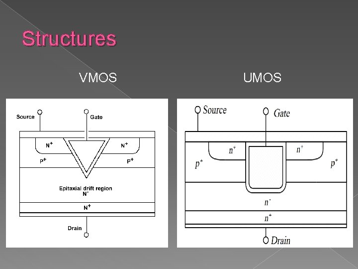
Structures VMOS UMOS
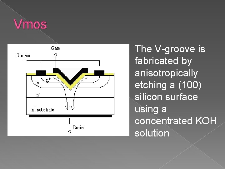
Vmos The V-groove is fabricated by anisotropically etching a (100) silicon surface using a concentrated KOH solution

Umos
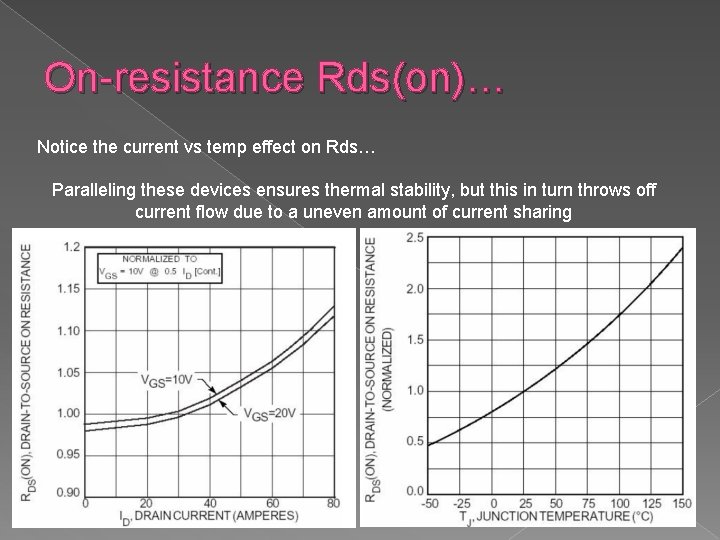
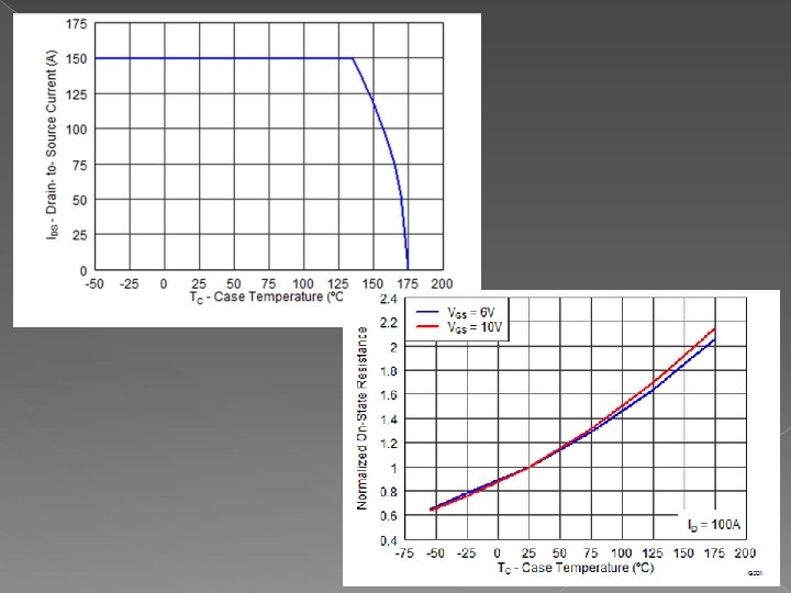
On-resistance Rds(on)… Notice the current vs temp effect on Rds… Paralleling these devices ensures thermal stability, but this in turn throws off current flow due to a uneven amount of current sharing
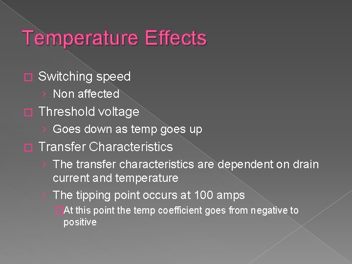
Temperature Effects � Switching speed › Non affected � Threshold voltage › Goes down as temp goes up � Transfer Characteristics › The transfer characteristics are dependent on drain current and temperature › The tipping point occurs at 100 amps �At this point the temp coefficient goes from negative to positive
Latch Up The act of being removed from powering the gate but the FET still operating.
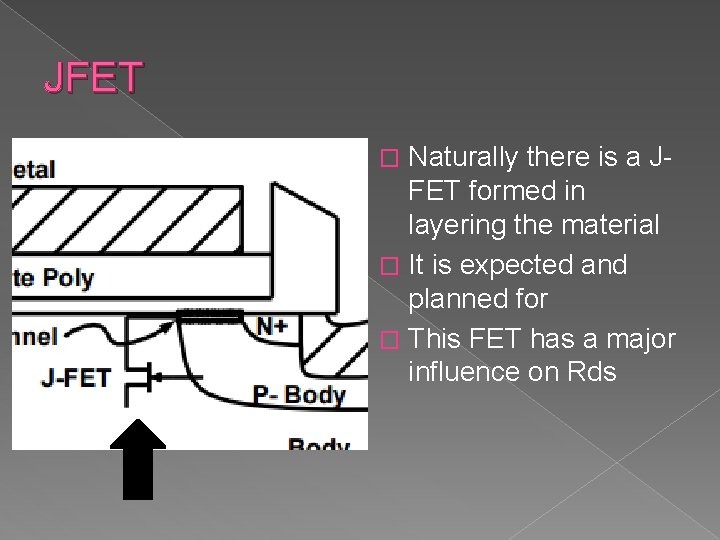
JFET Naturally there is a JFET formed in layering the material � It is expected and planned for � This FET has a major influence on Rds �
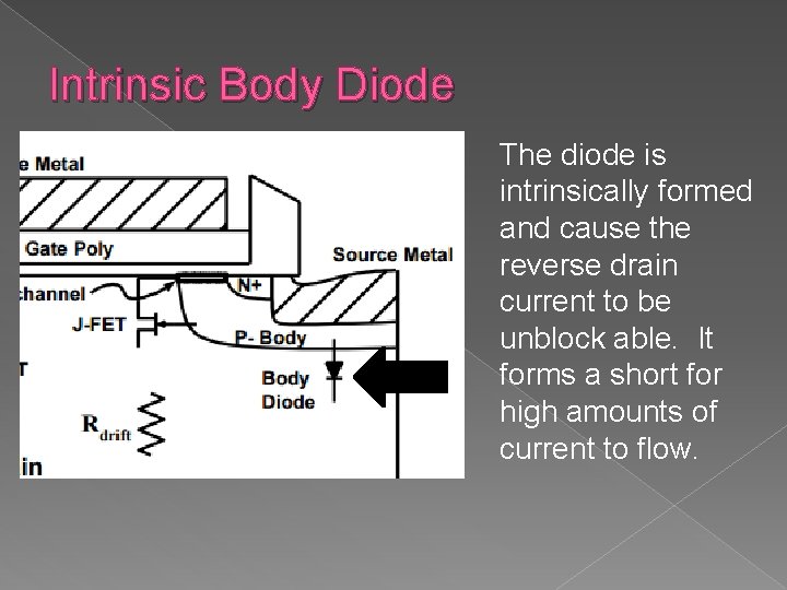
Intrinsic Body Diode The diode is intrinsically formed and cause the reverse drain current to be unblock able. It forms a short for high amounts of current to flow.
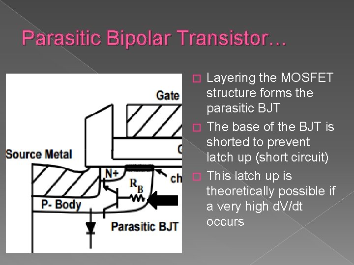
Parasitic Bipolar Transistor… Layering the MOSFET structure forms the parasitic BJT � The base of the BJT is shorted to prevent latch up (short circuit) � This latch up is theoretically possible if a very high d. V/dt occurs �
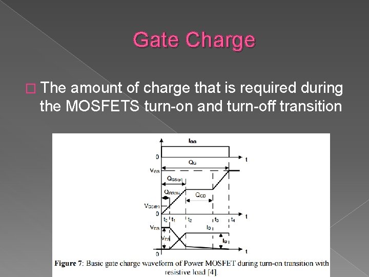
Gate Charge � The amount of charge that is required during the MOSFETS turn-on and turn-off transition
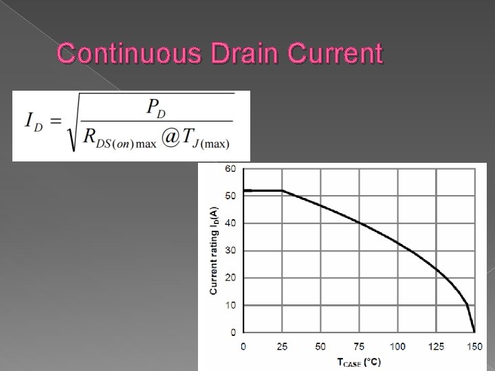
Continuous Drain Current
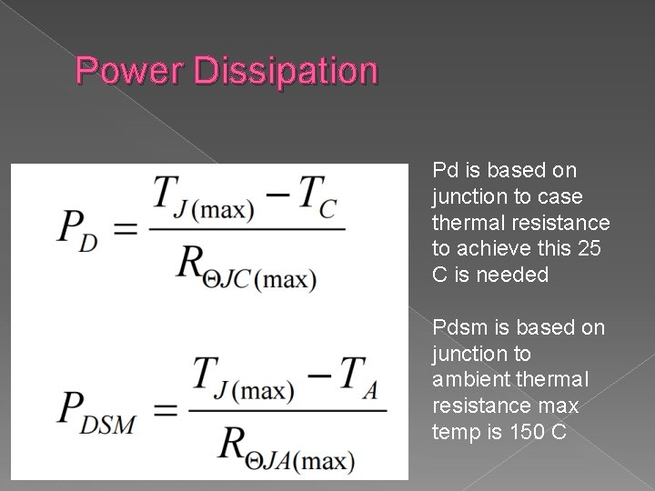
Power Dissipation Pd is based on junction to case thermal resistance to achieve this 25 C is needed Pdsm is based on junction to ambient thermal resistance max temp is 150 C
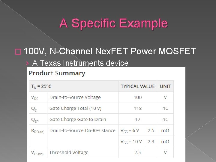
A Specific Example � 100 V, N-Channel Nex. FET Power MOSFET › A Texas Instruments device
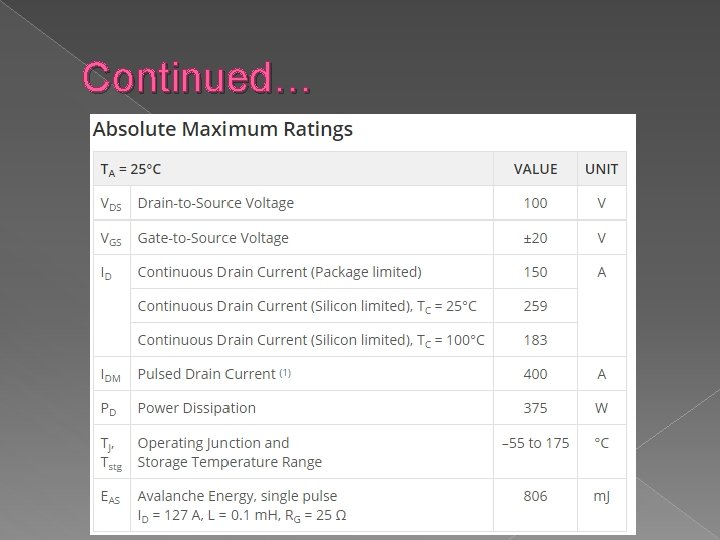
Continued…
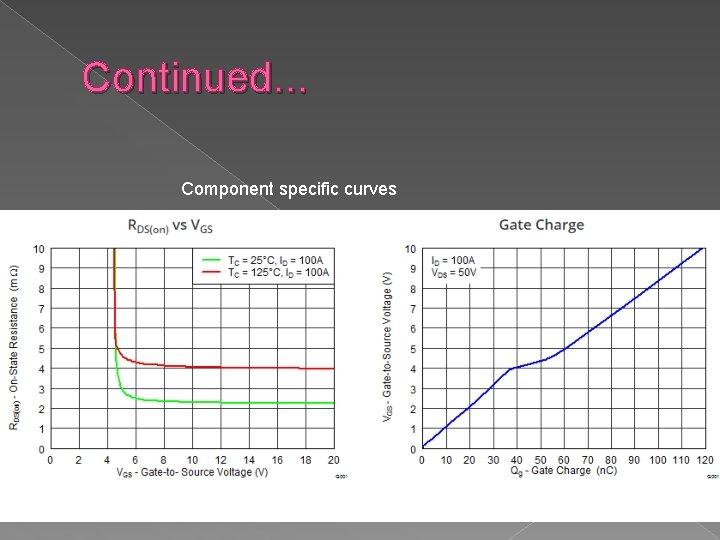
Continued. . . Component specific curves
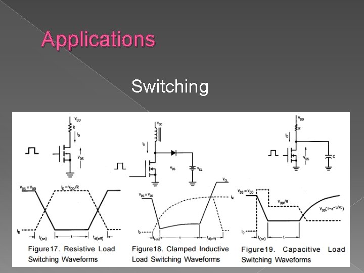
Applications Switching
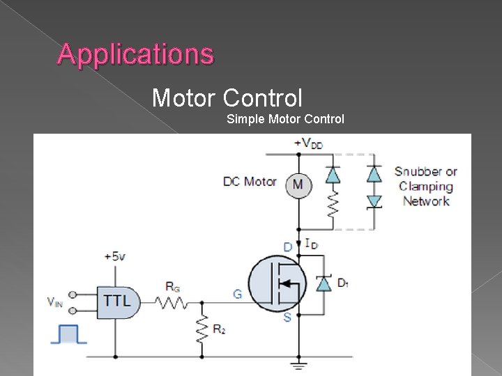
Applications Motor Control Simple Motor Control
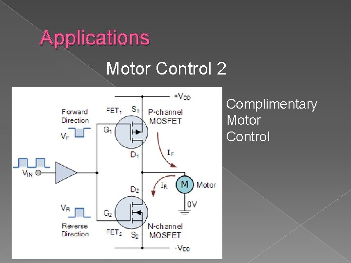
Applications Motor Control 2 Complimentary Motor Control
Conclusion � Power FET can handle more current and more voltage and current � The two types of FETs UMOS and VMOS � Can be Temperature dependent � The Effect of layering the material created certain desired and undesired elements � We looked at a specific Power FET � We saw some uses of the Power FET
Reference info � � � � � http: //www. aosmd. com/res/application_notes/mosfets/Power_M OSFET_Basics. pdf https: //www. fairchildsemi. com/application-notes/AN/AN-558. pdf http: //www. ixys. com/Documents/App. Notes/IXAN 0061. pdf Dpdge, Jonathan. “Power MOSFET Tutorial. ” 10 Mar. 2015. PDF file http: //web. iitd. ac. in/~mamidala/HTMLobj-1474/Trench-MOSFET -Book-Chapter-27 -Aug-12. pdf http: //www. ti. com/product/CSD 19536 KCS/datasheet http: //www. learningaboutelectronics. com/Articles/N-Channel. JFET-characteristics-curve http: //www. electronics-tutorials. ws/transistor/tran_7. html http: //ecee. colorado. edu/~bart/book/chapter 7/ch 7_8. htm
KEY CONCEPTS 1. 2. 3. 4. 5. Two types of FETS : UMOS and VMOS The channel etching occurs along certain lattice planes For use with High currents and Higher Voltages Temperature affects Threshold Voltage, Resistance and Transfer Characteristics Latch up, advantage and disadvantage

THA NK Y OU
- Slides: 30