Power estimation techniques and a new glitch filtering

- Slides: 37

Power estimation techniques and a new glitch filtering effect modeling based on probability waveform Fei Hu Department of Electrical and Computer Engineering, Auburn University, AL 36849 11/11/2004 Fei Hu, ELEC 6970 Fall 2004 1

Outline ¡ Introduction l ¡ Gate-level Probabilistic Approach l l ¡ l l 11/11/2004 Signal Probability Transition probability Transition density Probability waveform A new glitch filtering method l ¡ Different Levels of power estimation Based on Probability waveform The idea and examples Preliminary experimental results Summary Fei Hu, ELEC 6970 Fall 2004 2

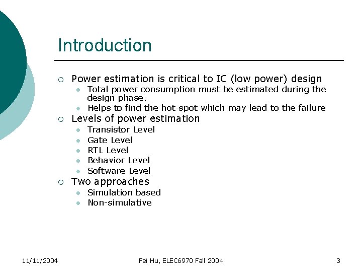
Introduction ¡ Power estimation is critical to IC (low power) design l l ¡ Levels of power estimation l l l ¡ Transistor Level Gate Level RTL Level Behavior Level Software Level Two approaches l l 11/11/2004 Total power consumption must be estimated during the design phase. Helps to find the hot-spot which may lead to the failure Simulation based Non-simulative Fei Hu, ELEC 6970 Fall 2004 3

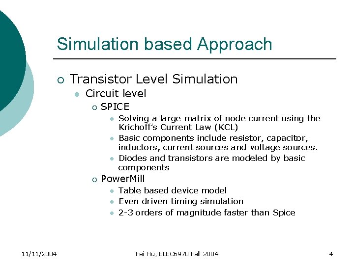
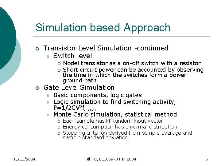
Simulation based Approach ¡ Transistor Level Simulation l Circuit level ¡ SPICE l l l ¡ Power. Mill l 11/11/2004 Solving a large matrix of node current using the Krichoff’s Current Law (KCL) Basic components include resistor, capacitor, inductors, current sources and voltage sources. Diodes and transistors are modeled by basic components Table based device model Even driven timing simulation 2 -3 orders of magnitude faster than Spice Fei Hu, ELEC 6970 Fall 2004 4

Simulation based Approach ¡ Transistor Level Simulation -continued l Switch level ¡ ¡ ¡ Gate Level Simulation l l l Basic components, logic gates Logic simulation to find switching activity, P=1/2 CV 2 factive Monte Carlo simulation, statistical method ¡ ¡ ¡ 11/11/2004 Model transistor as a on-off switch with a resistor Short circuit power can be accounted by observing the time in which the switches form a powerground path Each sample has N Random input vector Energy consumption has a normal distribution Stopping criterion derived from sample average and sample standard deviation Fei Hu, ELEC 6970 Fall 2004 5

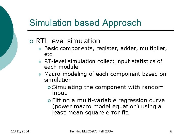
Simulation based Approach ¡ RTL level simulation l l l 11/11/2004 Basic components, register, adder, multiplier, etc. RT-level simulation collect input statistics of each module Macro-modeling of each component based on simulation ¡ Simulating the component with random input ¡ Fitting a multi-variable regression curve (power macro model equation) using a least mean square error fit. Fei Hu, ELEC 6970 Fall 2004 6

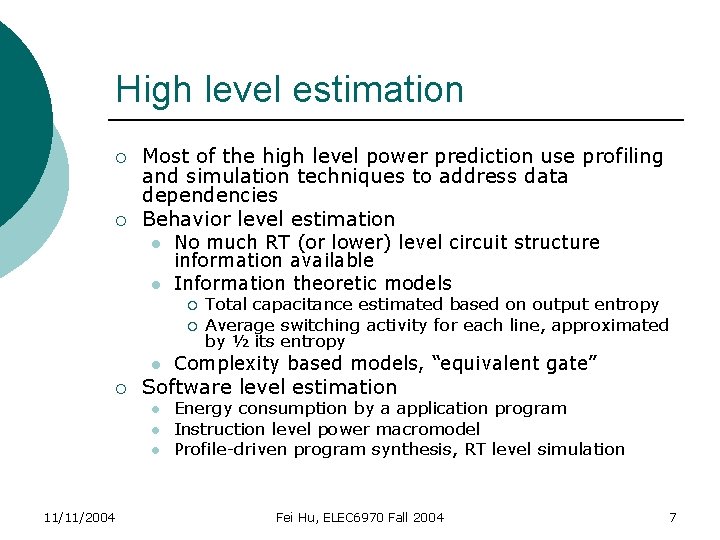
High level estimation ¡ ¡ Most of the high level power prediction use profiling and simulation techniques to address data dependencies Behavior level estimation l l No much RT (or lower) level circuit structure information available Information theoretic models ¡ ¡ l ¡ Complexity based models, “equivalent gate” Software level estimation l l l 11/11/2004 Total capacitance estimated based on output entropy Average switching activity for each line, approximated by ½ its entropy Energy consumption by a application program Instruction level power macromodel Profile-driven program synthesis, RT level simulation Fei Hu, ELEC 6970 Fall 2004 7

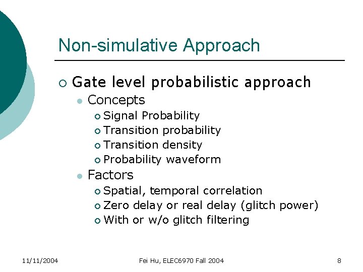
Non-simulative Approach ¡ Gate level probabilistic approach l Concepts Signal Probability ¡ Transition probability ¡ Transition density ¡ Probability waveform ¡ l Factors Spatial, temporal correlation ¡ Zero delay or real delay (glitch power) ¡ With or w/o glitch filtering ¡ 11/11/2004 Fei Hu, ELEC 6970 Fall 2004 8

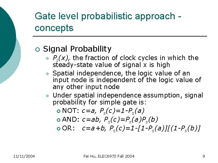
Gate level probabilistic approach concepts ¡ Signal Probability l l l 11/11/2004 Ps(x), the fraction of clock cycles in which the steady-state value of signal x is high Spatial independence, the logic value of an input node is independent of the logic value of any other input node Under spatial independence assumption, signal probability for simple gate is: ¡ NOT: c=a, Ps(c)=1 -Ps(a) ¡ AND: c=ab, Ps(c)=Ps(a)Ps(b) ¡ OR: c=a+b, Ps(c)=1 -[1 -Ps(a)][(1 -Ps(b)] Fei Hu, ELEC 6970 Fall 2004 9

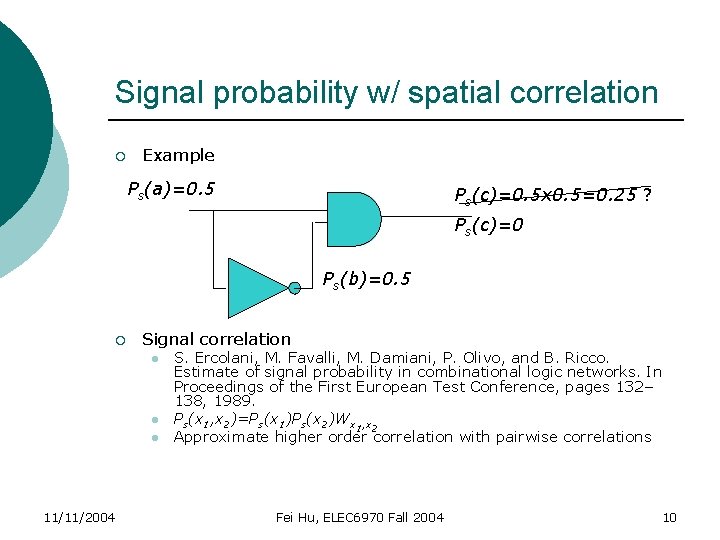
Signal probability w/ spatial correlation ¡ Example Ps(a)=0. 5 Ps(c)=0. 5 x 0. 5=0. 25 ? Ps(c)=0 Ps(b)=0. 5 ¡ Signal correlation l l l 11/11/2004 S. Ercolani, M. Favalli, M. Damiani, P. Olivo, and B. Ricco. Estimate of signal probability in combinational logic networks. In Proceedings of the First European Test Conference, pages 132– 138, 1989. Ps(x 1, x 2)=Ps(x 1)Ps(x 2)Wx 1, x 2 Approximate higher order correlation with pairwise correlations Fei Hu, ELEC 6970 Fall 2004 10

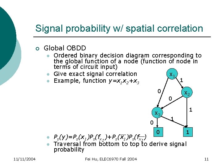
Signal probability w/ spatial correlation ¡ Global OBDD l l l Ordered binary decision diagram corresponding to the global function of a node (function of node in terms of circuit input) Give exact signal correlation x 1 1 Example, function y=x 1 x 2+x 3 0 0 x 3 0 l l 11/11/2004 0 x 2 1 1 1 Ps(y)=Ps(x 1)Ps(fx 1)+Ps(x 1)Ps(fx 1) Traversal from bottom to top to derive signal probability Fei Hu, ELEC 6970 Fall 2004 11

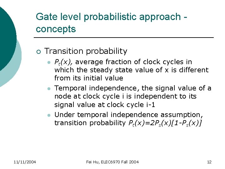
Gate level probabilistic approach concepts ¡ Transition probability l l l 11/11/2004 Pt(x), average fraction of clock cycles in which the steady state value of x is different from its initial value Temporal independence, the signal value of a node at clock cycle i is independent to its signal value at clock cycle i-1 Under temporal independence assumption, transition probability Pt(x)=2 Ps(x)[1 -Ps(x)] Fei Hu, ELEC 6970 Fall 2004 12

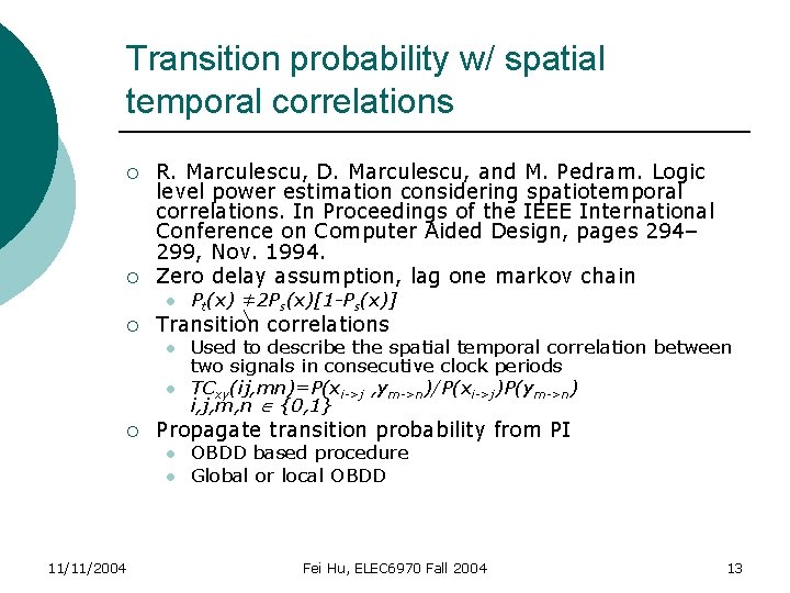
Transition probability w/ spatial temporal correlations ¡ ¡ R. Marculescu, D. Marculescu, and M. Pedram. Logic level power estimation considering spatiotemporal correlations. In Proceedings of the IEEE International Conference on Computer Aided Design, pages 294– 299, Nov. 1994. Zero delay assumption, lag one markov chain l ¡ Transition correlations l l ¡ Used to describe the spatial temporal correlation between two signals in consecutive clock periods TCxy(ij, mn)=P(xi->j , ym->n)/P(xi->j)P(ym->n) i, j, m, n {0, 1} Propagate transition probability from PI l l 11/11/2004 Pt(x) ≠ 2 Ps(x)[1 -Ps(x)] OBDD based procedure Global or local OBDD Fei Hu, ELEC 6970 Fall 2004 13

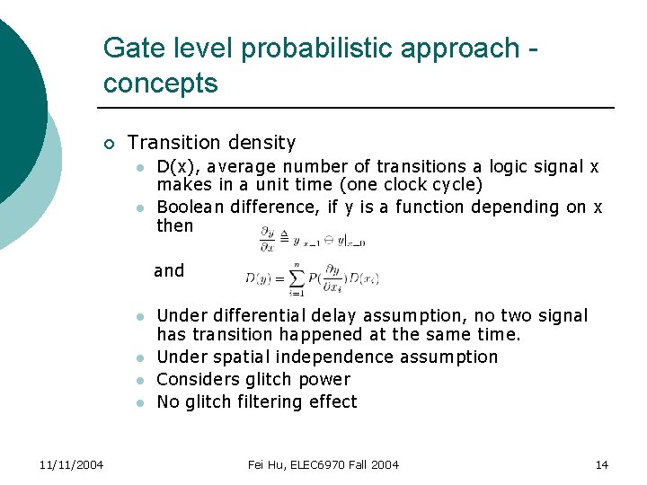
Gate level probabilistic approach concepts ¡ Transition density l l D(x), average number of transitions a logic signal x makes in a unit time (one clock cycle) Boolean difference, if y is a function depending on x then and l l 11/11/2004 Under differential delay assumption, no two signal has transition happened at the same time. Under spatial independence assumption Considers glitch power No glitch filtering effect Fei Hu, ELEC 6970 Fall 2004 14

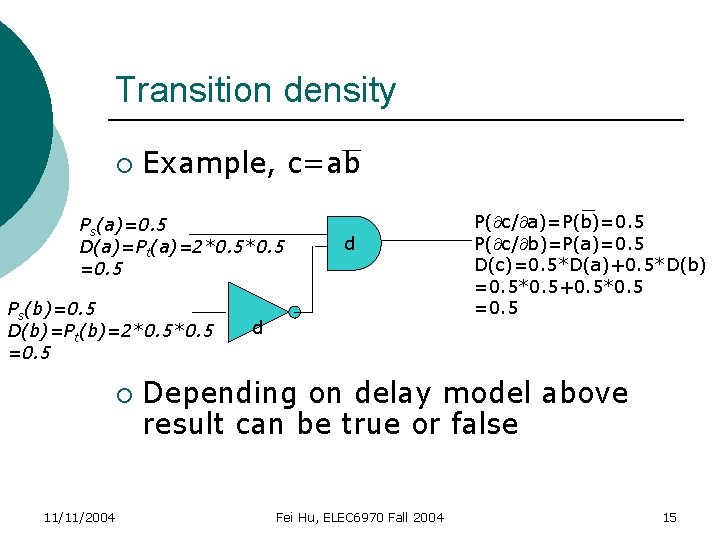
Transition density ¡ Example, c=ab Ps(a)=0. 5 D(a)=Pt(a)=2*0. 5 =0. 5 Ps(b)=0. 5 D(b)=Pt(b)=2*0. 5 =0. 5 ¡ 11/11/2004 d d P( c/ a)=P(b)=0. 5 P( c/ b)=P(a)=0. 5 D(c)=0. 5*D(a)+0. 5*D(b) =0. 5*0. 5+0. 5*0. 5 =0. 5 Depending on delay model above result can be true or false Fei Hu, ELEC 6970 Fall 2004 15

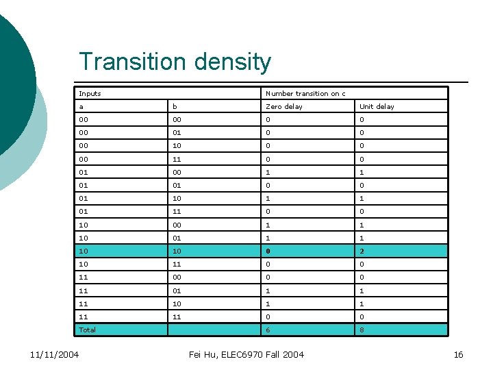
Transition density Inputs a b Zero delay Unit delay 00 00 01 0 0 00 10 0 0 00 11 0 0 01 00 1 1 01 01 0 0 01 10 1 1 01 11 0 0 10 00 1 1 10 01 1 1 10 10 0 2 10 11 00 0 0 11 01 1 1 11 10 1 1 11 11 0 0 6 8 Total 11/11/2004 Number transition on c Fei Hu, ELEC 6970 Fall 2004 16

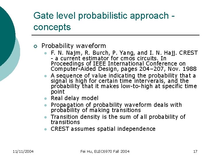
Gate level probabilistic approach concepts ¡ Probability waveform l l l 11/11/2004 F. N. Najm, R. Burch, P. Yang, and I. N. Hajj. CREST - a current estimator for cmos circuits. In Proceedings of IEEE International Conference on Computer-Aided Design, pages 204– 207, Nov. 1988 A sequence of value indicating the probability that a signal is high for certain time interverals, and the probability that it makes low-to-high at specific time point Real delay model Propagation of probability waveform deals with probability of making transitions Transition density is the sum of all probability of transitions CREST assumes spatial independence Fei Hu, ELEC 6970 Fall 2004 17

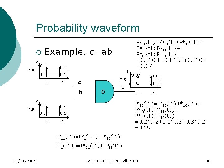
Probability waveform ¡ P 0. 5 Example, c=ab 0. 1 0. 2 0. 1 t 2 P 0. 5 0. 1 0. 2 0. 1 t 1 0. 5 a b P Pc 01(t 1)=Pa 01(t 1) Pb 01(t 1)+ Pa 01(t 1) Pb 11(t 1)+ Pa 11(t 1) Pb 01(t 1) =0. 1*0. 1+0. 1*0. 3+0. 3*0. 1 =0. 07 0 c 0. 07 0. 16 t 1 0. 16 0. 07 t 2 Pc 10(t 1)=Pa 10(t 1) Pb 10(t 1)+ Pa 10(t 1) Pb 11(t 1)+ Pa 11(t 1) Pb 10(t 1) =0. 2*0. 2+0. 2*0. 3+0. 3*0. 2 =0. 16 t 2 Pc 11(t 1)=Pc 1(t 1 -)- Pc 10(t 1) Pc 1(t 1+)=Pc 01(t 1)+Pc 11(t 1) 11/11/2004 Fei Hu, ELEC 6970 Fall 2004 18

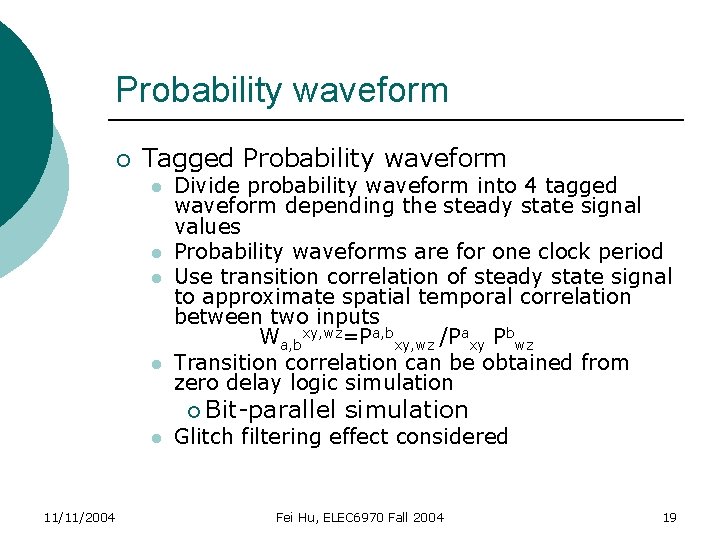
Probability waveform ¡ Tagged Probability waveform l l Divide probability waveform into 4 tagged waveform depending the steady state signal values Probability waveforms are for one clock period Use transition correlation of steady state signal to approximate spatial temporal correlation between two inputs Wa, bxy, wz=Pa, bxy, wz /Paxy Pbwz Transition correlation can be obtained from zero delay logic simulation ¡ Bit-parallel simulation l 11/11/2004 Glitch filtering effect considered Fei Hu, ELEC 6970 Fall 2004 19

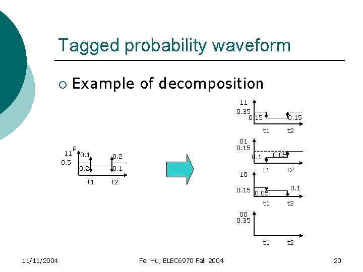
Tagged probability waveform ¡ Example of decomposition 11 0. 35 0. 15 t 1 11 0. 5 P 01 0. 15 0. 1 0. 2 0. 1 t 1 0. 05 0. 1 10 t 2 t 1 0. 15 0. 05 t 2 0. 1 t 2 t 1 t 2 00 0. 35 11/11/2004 Fei Hu, ELEC 6970 Fall 2004 20

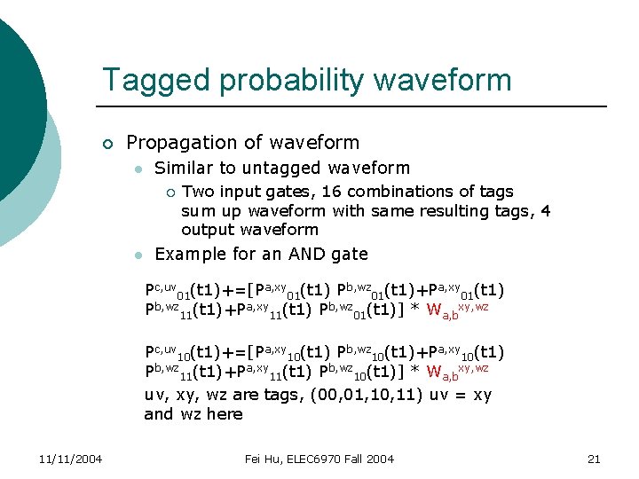
Tagged probability waveform ¡ Propagation of waveform l Similar to untagged waveform ¡ l Two input gates, 16 combinations of tags sum up waveform with same resulting tags, 4 output waveform Example for an AND gate Pc, uv 01(t 1)+=[Pa, xy 01(t 1) Pb, wz 01(t 1)+Pa, xy 01(t 1) Pb, wz 11(t 1)+Pa, xy 11(t 1) Pb, wz 01(t 1)] * Wa, bxy, wz Pc, uv 10(t 1)+=[Pa, xy 10(t 1) Pb, wz 10(t 1)+Pa, xy 10(t 1) Pb, wz 11(t 1)+Pa, xy 11(t 1) Pb, wz 10(t 1)] * Wa, bxy, wz uv, xy, wz are tags, (00, 01, 10, 11) uv = xy and wz here 11/11/2004 Fei Hu, ELEC 6970 Fall 2004 21

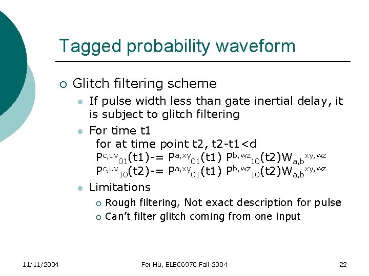
Tagged probability waveform ¡ Glitch filtering scheme l l l If pulse width less than gate inertial delay, it is subject to glitch filtering For time t 1 for at time point t 2, t 2 -t 1<d Pc, uv 01(t 1)-= Pa, xy 01(t 1) Pb, wz 10(t 2)Wa, bxy, wz Pc, uv (t 2)-= Pa, xy (t 1) Pb, wz (t 2)W xy, wz 10 01 10 a, b Limitations ¡ ¡ 11/11/2004 Rough filtering, Not exact description for pulse Can’t filter glitch coming from one input Fei Hu, ELEC 6970 Fall 2004 22

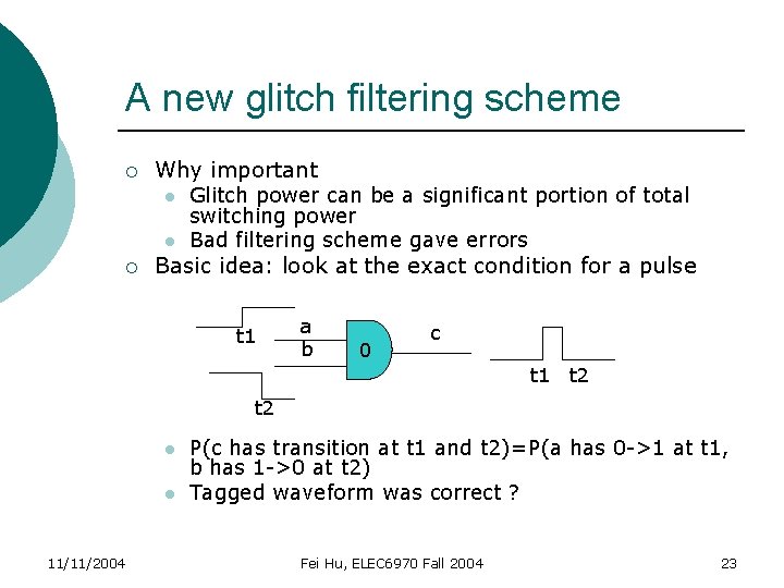
A new glitch filtering scheme ¡ Why important l l ¡ Glitch power can be a significant portion of total switching power Bad filtering scheme gave errors Basic idea: look at the exact condition for a pulse t 1 a b 0 c t 1 t 2 l l 11/11/2004 P(c has transition at t 1 and t 2)=P(a has 0 ->1 at t 1, b has 1 ->0 at t 2) Tagged waveform was correct ? Fei Hu, ELEC 6970 Fall 2004 23

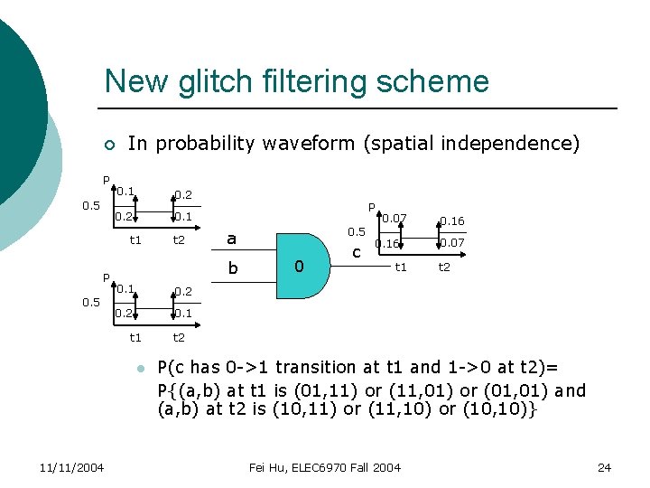
New glitch filtering scheme ¡ P 0. 5 In probability waveform (spatial independence) 0. 1 0. 2 0. 1 t 1 P 0. 5 0. 1 0. 2 0. 1 l 0. 5 a b t 1 11/11/2004 t 2 P 0 c 0. 07 0. 16 t 1 0. 16 0. 07 t 2 P(c has 0 ->1 transition at t 1 and 1 ->0 at t 2)= P{(a, b) at t 1 is (01, 11) or (11, 01) or (01, 01) and (a, b) at t 2 is (10, 11) or (11, 10) or (10, 10)} Fei Hu, ELEC 6970 Fall 2004 24

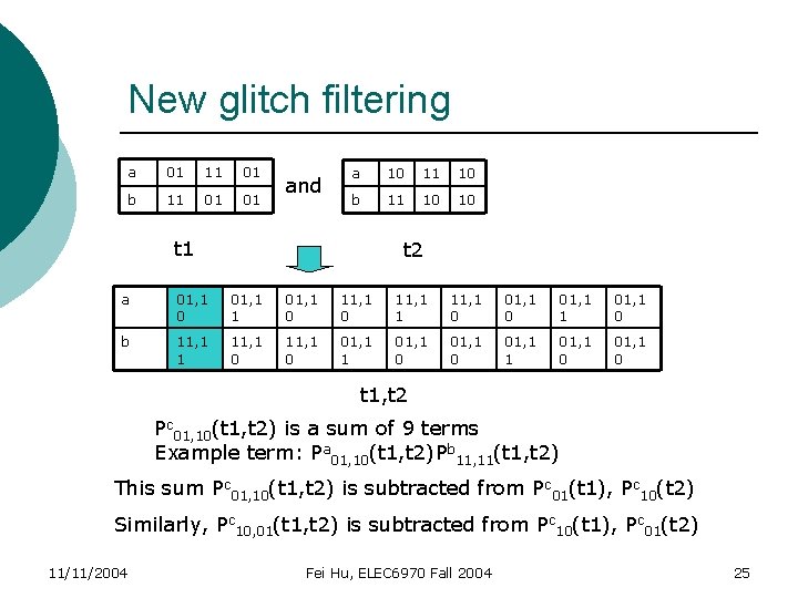
New glitch filtering a 01 11 01 b 11 01 01 and a 10 11 10 b 11 10 10 t 1 t 2 a 01, 1 0 01, 1 1 01, 1 0 11, 1 1 11, 1 0 01, 1 1 01, 1 0 b 11, 1 1 11, 1 0 01, 1 1 01, 1 0 t 1, t 2 Pc 01, 10(t 1, t 2) is a sum of 9 terms Example term: Pa 01, 10(t 1, t 2)Pb 11, 11(t 1, t 2) This sum Pc 01, 10(t 1, t 2) is subtracted from Pc 01(t 1), Pc 10(t 2) Similarly, Pc 10, 01(t 1, t 2) is subtracted from Pc 10(t 1), Pc 01(t 2) 11/11/2004 Fei Hu, ELEC 6970 Fall 2004 25

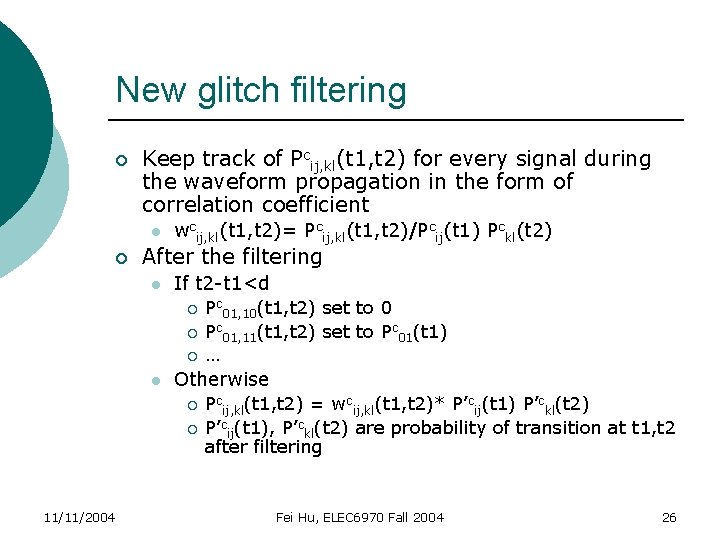
New glitch filtering ¡ Keep track of Pcij, kl(t 1, t 2) for every signal during the waveform propagation in the form of correlation coefficient l ¡ wcij, kl(t 1, t 2)= Pcij, kl(t 1, t 2)/Pcij(t 1) Pckl(t 2) After the filtering l If t 2 -t 1<d ¡ ¡ ¡ l Otherwise ¡ ¡ 11/11/2004 Pc 01, 10(t 1, t 2) set to 0 Pc 01, 11(t 1, t 2) set to Pc 01(t 1) … Pcij, kl(t 1, t 2) = wcij, kl(t 1, t 2)* P’cij(t 1) P’ckl(t 2) P’cij(t 1), P’ckl(t 2) are probability of transition at t 1, t 2 after filtering Fei Hu, ELEC 6970 Fall 2004 26

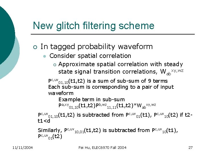
New glitch filtering scheme ¡ In tagged probability waveform l Consider spatial correlation ¡ Approximate spatial correlation with steady state signal transition correlations, Wabxy, wz Pc, uv 01, 10(t 1, t 2) is a sum of sub-sum of 9 terms Each sub-sum is corresponding to a pair of input waveform Example term in sub-sum Pa, xy 01, 10(t 1, t 2)Pb, wz 11, 11(t 1, t 2)*Wabxy, wz Pc, uv 01, 10(t 1, t 2) is subtracted from Pc, uv 01(t 1), Pc, uv 10(t 2) if t 2 t 1<d Similarly, Pc, uv 10, 01(t 1, t 2) is subtracted from Pc, uv 10(t 1), Pc, uv 01(t 2) 11/11/2004 Fei Hu, ELEC 6970 Fall 2004 27

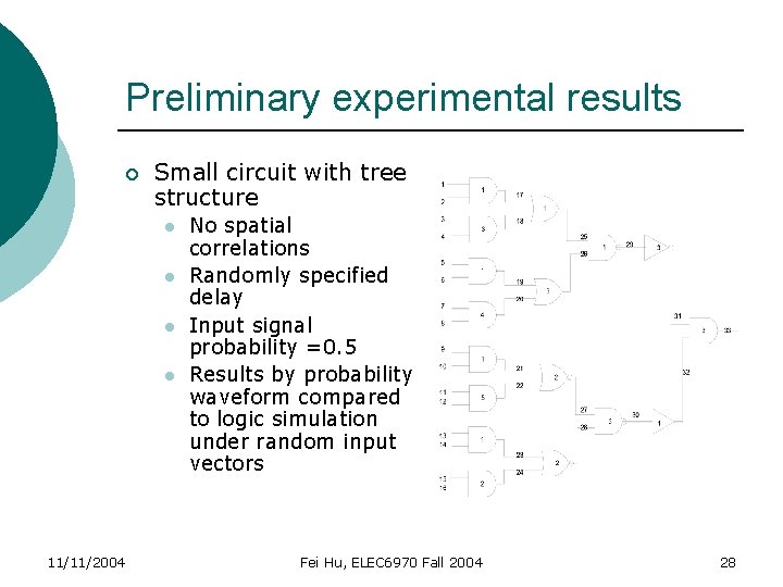
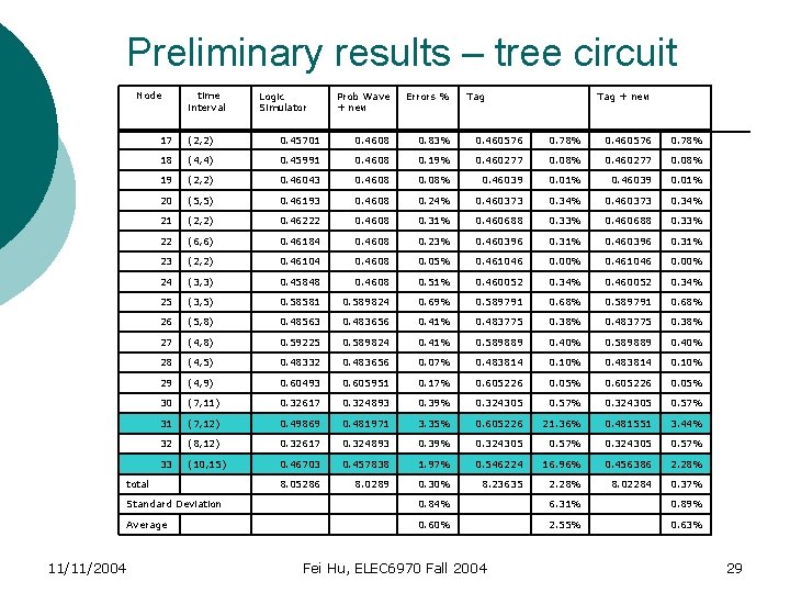
Preliminary experimental results ¡ Small circuit with tree structure l l 11/11/2004 No spatial correlations Randomly specified delay Input signal probability =0. 5 Results by probability waveform compared to logic simulation under random input vectors Fei Hu, ELEC 6970 Fall 2004 28

Preliminary results – tree circuit Node Logic Simulator Prob Wave + new Errors % Tag + new 17 (2, 2) 0. 45701 0. 4608 0. 83% 0. 460576 0. 78% 18 (4, 4) 0. 45991 0. 4608 0. 19% 0. 460277 0. 08% 19 (2, 2) 0. 46043 0. 4608 0. 08% 0. 46039 0. 01% 20 (5, 5) 0. 46193 0. 4608 0. 24% 0. 460373 0. 34% 21 (2, 2) 0. 46222 0. 4608 0. 31% 0. 460688 0. 33% 22 (6, 6) 0. 46184 0. 4608 0. 23% 0. 460396 0. 31% 23 (2, 2) 0. 46104 0. 4608 0. 05% 0. 461046 0. 00% 24 (3, 3) 0. 45848 0. 4608 0. 51% 0. 460052 0. 34% 25 (3, 5) 0. 58581 0. 589824 0. 69% 0. 589791 0. 68% 26 (5, 8) 0. 48563 0. 483656 0. 41% 0. 483775 0. 38% 27 (4, 8) 0. 59225 0. 589824 0. 41% 0. 589889 0. 40% 28 (4, 5) 0. 48332 0. 483656 0. 07% 0. 483814 0. 10% 29 (4, 9) 0. 60493 0. 605951 0. 17% 0. 605226 0. 05% 30 (7, 11) 0. 32617 0. 324893 0. 39% 0. 324305 0. 57% 31 (7, 12) 0. 49869 0. 481971 3. 35% 0. 605226 21. 36% 0. 481551 3. 44% 32 (8, 12) 0. 32617 0. 324893 0. 39% 0. 324305 0. 57% 33 (10, 15) 0. 46703 0. 457838 1. 97% 0. 546224 16. 96% 0. 456386 2. 28% 8. 05286 8. 0289 0. 30% 8. 23635 2. 28% 8. 02284 0. 37% total 11/11/2004 time interval Standard Deviation 0. 84% 6. 31% 0. 89% Average 0. 60% 2. 55% 0. 63% Fei Hu, ELEC 6970 Fall 2004 29

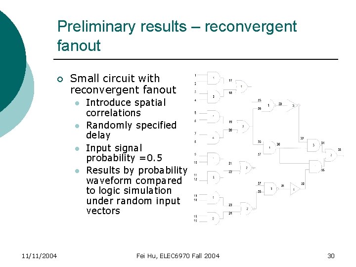
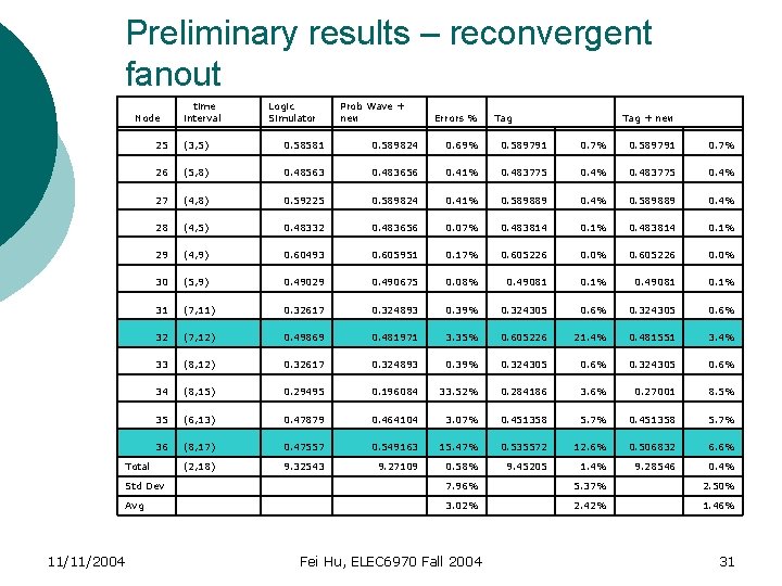
Preliminary results – reconvergent fanout ¡ Small circuit with reconvergent fanout l l 11/11/2004 Introduce spatial correlations Randomly specified delay Input signal probability =0. 5 Results by probability waveform compared to logic simulation under random input vectors Fei Hu, ELEC 6970 Fall 2004 30

Preliminary results – reconvergent fanout Node 11/11/2004 time interval Logic Simulator Prob Wave + new Errors % Tag + new 25 (3, 5) 0. 58581 0. 589824 0. 69% 0. 589791 0. 7% 26 (5, 8) 0. 48563 0. 483656 0. 41% 0. 483775 0. 4% 27 (4, 8) 0. 59225 0. 589824 0. 41% 0. 589889 0. 4% 28 (4, 5) 0. 48332 0. 483656 0. 07% 0. 483814 0. 1% 29 (4, 9) 0. 60493 0. 605951 0. 17% 0. 605226 0. 0% 30 (5, 9) 0. 49029 0. 490675 0. 08% 0. 49081 0. 1% 31 (7, 11) 0. 32617 0. 324893 0. 39% 0. 324305 0. 6% 32 (7, 12) 0. 49869 0. 481971 3. 35% 0. 605226 21. 4% 0. 481551 3. 4% 33 (8, 12) 0. 32617 0. 324893 0. 39% 0. 324305 0. 6% 34 (8, 15) 0. 29495 0. 196084 33. 52% 0. 284186 3. 6% 0. 27001 8. 5% 35 (6, 13) 0. 47879 0. 464104 3. 07% 0. 451358 5. 7% 36 (8, 17) 0. 47557 0. 549163 15. 47% 0. 535572 12. 6% 0. 506832 6. 6% Total (2, 18) 9. 32543 9. 27109 0. 58% 9. 45205 1. 4% 9. 28546 0. 4% Std Dev 7. 96% 5. 37% 2. 50% Avg 3. 02% 2. 42% 1. 46% Fei Hu, ELEC 6970 Fall 2004 31

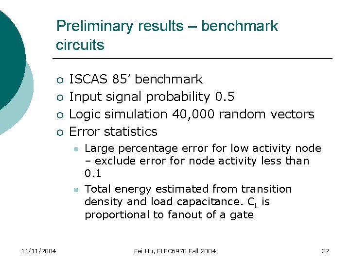
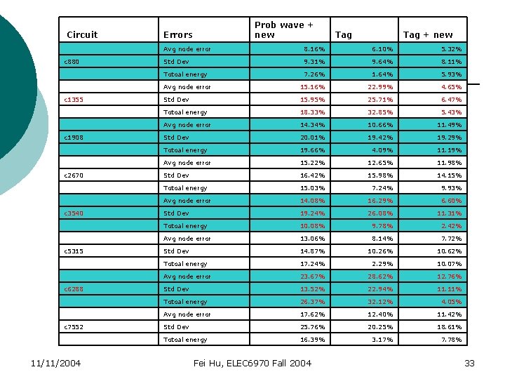
Preliminary results – benchmark circuits ¡ ¡ ISCAS 85’ benchmark Input signal probability 0. 5 Logic simulation 40, 000 random vectors Error statistics l l 11/11/2004 Large percentage error for low activity node – exclude error for node activity less than 0. 1 Total energy estimated from transition density and load capacitance. CL is proportional to fanout of a gate Fei Hu, ELEC 6970 Fall 2004 32

Prob wave + new Circuit Errors Avg node error 8. 16% 6. 10% 5. 32% c 880 Std Dev 9. 31% 9. 64% 8. 11% Totoal energy 7. 26% 1. 64% 5. 93% Avg node error 15. 16% 22. 99% 4. 65% c 1355 Std Dev 15. 95% 25. 71% 6. 47% Totoal energy 18. 33% 32. 85% 5. 43% Avg node error 14. 34% 10. 66% 11. 49% c 1908 Std Dev 20. 01% 19. 42% 19. 29% Totoal energy 19. 66% 4. 09% 11. 19% Avg node error 15. 22% 12. 65% 11. 98% c 2670 Std Dev 16. 42% 15. 98% 14. 15% Totoal energy 15. 03% 7. 24% 9. 93% Avg node error 14. 08% 16. 29% 6. 60% c 3540 Std Dev 19. 24% 26. 08% 11. 31% Totoal energy 10. 08% 9. 78% 2. 42% Avg node error 13. 06% 8. 14% 7. 72% c 5315 Std Dev 14. 87% 10. 26% 10. 62% Totoal energy 17. 24% 2. 29% 10. 07% Avg node error 23. 67% 28. 62% 12. 76% c 6288 Std Dev 13. 52% 22. 94% 11. 11% Totoal energy 26. 37% 32. 12% 4. 05% Avg node error 17. 62% 12. 40% 11. 42% c 7552 Std Dev 25. 76% 20. 25% 18. 61% Totoal energy 16. 39% 3. 17% 7. 78% 11/11/2004 Fei Hu, ELEC 6970 Fall 2004 Tag + new 33

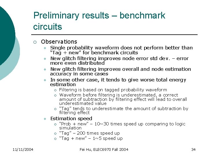
Preliminary results – benchmark circuits ¡ Observations l l Single probability waveform does not perform better than “Tag + new” for benchmark circuits New glitch filtering improves node error std dev. – error more even distributed New glitch filtering improves overall and node estimation accuracy in some cases In some other case, it tends to give worse total energy estimation ¡ ¡ ¡ l Estimation speed ¡ ¡ ¡ 11/11/2004 Filtering is based on tagged probability waveform Waveform before filtering is underestimated, a correct amount of subtraction by filtering effect will lead to overall underestimated value “Tag” tends to underestimate the amount of subtraction by filtering effect “Prob + new” – 10~30 times speed up comparing to logic simulation “Tag” – 200 times speed up “Tag + new” – 1~5 speed up Fei Hu, ELEC 6970 Fall 2004 34

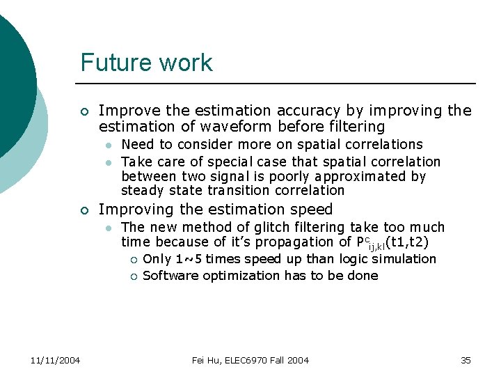
Future work ¡ Improve the estimation accuracy by improving the estimation of waveform before filtering l l ¡ Need to consider more on spatial correlations Take care of special case that spatial correlation between two signal is poorly approximated by steady state transition correlation Improving the estimation speed l The new method of glitch filtering take too much time because of it’s propagation of Pcij, kl(t 1, t 2) ¡ ¡ 11/11/2004 Only 1~5 times speed up than logic simulation Software optimization has to be done Fei Hu, ELEC 6970 Fall 2004 35

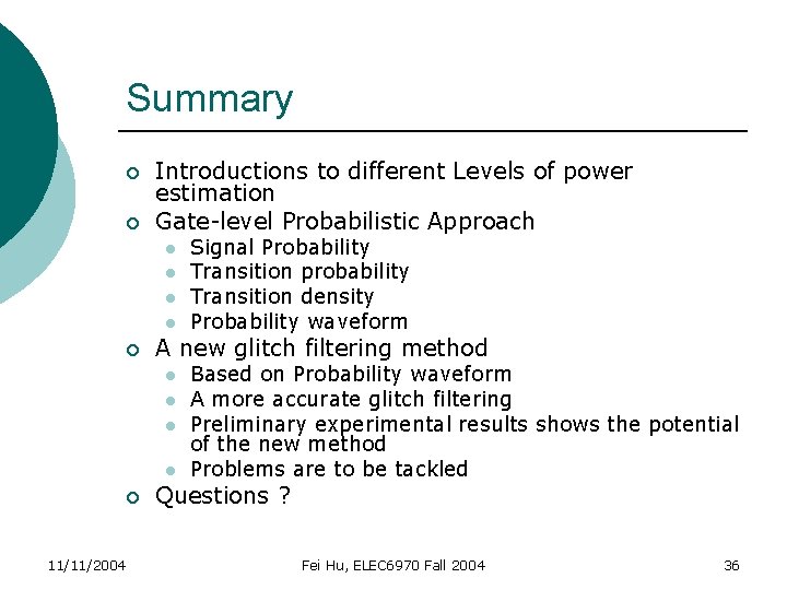
Summary ¡ ¡ Introductions to different Levels of power estimation Gate-level Probabilistic Approach l l ¡ A new glitch filtering method l l ¡ 11/11/2004 Signal Probability Transition probability Transition density Probability waveform Based on Probability waveform A more accurate glitch filtering Preliminary experimental results shows the potential of the new method Problems are to be tackled Questions ? Fei Hu, ELEC 6970 Fall 2004 36

Thank You ! For questions and comments, please contact me at hufei 01@auburn. edu 11/11/2004 Fei Hu, ELEC 6970 Fall 2004 37