POWER DISTRIBUTION Interconnect properties Not all metal layers

POWER DISTRIBUTION

Interconnect properties • Not all metal layers have the same properties: – Hard to fabricate small-pitch metal on higher layers. • Match the uses of each layer to its performance and power properties.

Levels of interconnect global 6 X 2 X local 1 X

Resistance vs. size • Increasing width struggles scaling in resistance. – Constant scaling increases resistance quadratically. • n. X layers are larger, can support fewer wires per square centimeter. • Use higher layers for global power and signals.

Wire design • Long global signals usually require repeaters. – The transistors are on the silicon layer---must use vias to go all the way down and back up. • Thermal gradients can exist horizontally and to some extent vertically.

Power distribution • Must size wires to be able to handle current— requires designing topology of VDD/VSS networks. • Want to keep power network in metal— requires designing planar wiring. • Power distribution problems: – IR drops from steady state current. – L di/dt drops from transient current.

Power Distribution Network • Ohmic drops that degrade the signal level are especially important in the power distribution network where current levels can easily reach amperes. • Such IR drops – affect reliability – impact the performance as even a small drop in VDD can cause a significant increase in delay

• Design the techniques for power distribution networks to Reduce the maximum distance between the supply pins and the circuit supply connections by adopting a structured layout of the power distribution network • route power and ground vertically (or horizontally) interdigitized on the same layer bringing power in from two sides of the die • use two metal layers for power distribution bringing power in from four sides of the die • use two solid metal planes for distribution of VDD and GND – Size the power network appropriately

Interdigitated power and ground lines VDD VSS

Power tree design • Each branch must be able to supply required current to all of its subsidiary branches: • Trees are interdigitated to supply both sides of power supply.

Planar power/ground routing theorem • Draw a dividing line through each cell such that all VDD terminals are on one side and all VSS terminals on the other. • If floorplan places all cells with VDD on same side, there exists a routing for both VDD and VSS which does not require them to cross. VSS VDD cell VSS VDD

Planar routing theorem example cut line VSS VDD B VDD VSS no cut line C VDD VSS A VDD VSS no connection cut line VDD VSS

Power supply noise • Variations in power supply voltage manifest themselves as noise into the logic gates. • Power supply wiring resistance creates voltage variations with current surges. • Voltage drops on power lines depend on dynamic behavior of circuit.

Tackling power supply noise • Must measure current required by each block at varying times. • May need to redesign power/ground network to reduce resistance at high current loads. • Worst case, may have to move some activity to another clock cycle to reduce peak current.

Power distribution grids • Upper layers carry global power to subsystems. • Lower layers distribute to smaller blocks. • Physical design: – Within a layer, interdigitate VDD/VSS. – Between layers, put power lines orthogonally.

Decoupling capacitors

Clock distribution • Goals: – deliver clock to all memory elements with acceptable skew; – deliver clock edges with acceptable sharpness. • Clocking network design is one of the greatest challenges in the design of a large chip.

Clock delay varies with position

H-tree f

Clock distribution tree • Clocks are generally distributed via wiring trees. • Want to use low-resistance interconnect to minimize delay. • Use multiple drivers to distribute driver requirements—use optimal sizing principles to design buffers. • Clock lines can create significant crosstalk.

Clock distribution tree example

Floorplanning tips • Develop a wiring plan. Think about how layers will be used to distribute important wires. • Sweep small components into larger blocks. A floorplan with a single NAND gate in the middle will be hard to work with. • Design wiring that looks simple. If it looks complicated, it is complicated.

Floorplanning tips, cont’d. • Design planar wiring. Planarity is the essence of simplicity. It isn’t always possible, but do it where feasible (and where it doesn’t introduce unacceptable delay). • Draw separate wiring plans for power and clocking. These are important design tasks which should be tackled early.

Cross talk Unwanted coupling with adjacent signal wires injects noise into a signal depending on the transient values of the other signals routed in the neighborhood

Power optimization • Glitches cause unnecessary power consumption. • Logic network design helps control power consumption: – minimizing capacitance; – eliminating unnecessary glitches.

Glitching example • Gate network:

Glitching example behavior • NOR gate produces 0 output at beginning and end: – beginning: bottom input is 1; – end: NAND output is 1; • Difference in delay between application of primary inputs and generation of new NAND output causes glitch.

Adder chain glitching bad good

Explanation • Unbalanced chain has signals arriving at different times at each adder. • A glitch downstream propagates all the way upstream. • Balanced tree introduces multiple glitches simultaneously, reducing total glitch activity.

Signal probabilities • Glitching behavior can be characterized by signal probabilities. • Transition probabilities can be computed from signal probabilities if clock cycles are assumed to be independent. • Some primary inputs may have non-standard signal probabilities— control signal may be activated only occasionally.

Delay-independent probabilities • Compute output probabilities of primitive functions: – PNOT = 1 - Pin – POR = 1 - Pi) – PAND = Pi • Can compute output probabilities of re convergent fanout-free networks by traversing tree.

Factorization techniques • In example, a has high transition probability, b and c low probabilities. • Reduce number of logic levels through which high-probability signals must travel in order to reduce propagation of glitches.


Wires and vias • • Wire and via structures. Wire parasitics. Transistor parasitics. Fabrication theory and practice.

Wires and vias metal 3 metal 2 vias metal 1 poly n+ p-tub poly n+

Metal interconnect • Many layers of metal interconnect are possible. – 12 layers of metal are common. • Lower layers have smaller features, higher layers have larger features. • Can’t directly go from a layer to any other layer.

Copper interconnect • Much better electrical characteristics. • Copper is poisonous to semiconductors---must be isolated from silicon. – Bottom layer of interconnect is aluminum.

Metal migration • Current-carrying capacity of metal wire depends on cross-section. • Height is fixed, so width determines current limit. • Metal migration: when current is too high, electron flow pushes around metal grains. • Higher resistance increases metal migration, leading to destruction of wire.

Metal migration problems and solutions • Marginal wires will fail after a small operating period. • Normal wires must be sized to accommodate maximum current flow: Imax = 1. 5 m. A/ m of metal width. • Mainly applies to VDD/VSS lines.

wiring capacitance • The wiring capacitance depends upon the length and width of the connecting wires and is a function of the fan-out from the driving gate and the number of fan-out gates. • Wiring capacitance is growing in importance with the scaling of technology.
 dielectrics (insulators) such as polymide or even")
Dealing with Capacitance • Low capacitance (low-k) dielectrics (insulators) such as polymide or even air instead of Si. O 2 – family of materials that are low-k dielectrics – must also be suitable thermally and mechanically and – compatible with (copper) interconnect • Copper interconnect allows wires to be thinner without increasing their resistance, thereby decreasing interwire capacitance • SOI (silicon on insulator) to reduce junction capacitance 42
 substrate")
Diffusion wire capacitance • Capacitances formed by p-n junctions: sidewall capacitances n+ (ND) substrate (NA) bottomwall capacitance depletion region

Depletion region capacitance • Zero-bias depletion capacitance: – Cj 0 = si/xd. • Depletion region width: – xd 0 = sqrt[(1/NA + 1/ND)2 si. Vbi/q]. • Junction capacitance is function of voltage across junction: – Cj(Vr) = Cj 0/sqrt(1 + Vr/Vbi)

Poly/metal wire capacitance • Two components: – parallel plate; – fringe plate

• Fringe capacitance is the capacitance due to the stray electric fields at the edges of a capacitor. • Think of the parallel plate capacitor, where the electric field lines in the center are straight. • The edges of the plates have fringing fields. • The capacitance due to the field at the edges is the fringe capacitance. • In the case of interconnect capacitance, the metal lines on the chip will cross over each other and form parallel plate capacitors, with edges.

Metal coupling capacitances • Can couple to adjacent wires on same layer, wires on above/below layers: metal 2 metal 1

Example: parasitic capacitance measurement • n-diffusion: bottomwall=2 f. F, sidewall=2 f. F. • metal: plate=0. 15 f. F, 1. 5 m fringe=0. 72 f. F. 3 m 0. 75 m 1 m 2. 5 m

Wire resistance • Resistance of any size square is constant:

Wire Spacing Comparisons Intel P 858 Al, 0. 18 m Intel P 856. 5 Al, 0. 25 m - 0. 07 - 0. 05 - 0. 12 M 4 - 0. 33 M 3 - 0. 33 M 2 - 1. 11 Scale: 2, 160 nm M 6 M 5 - 0. 08 M 1 M 5 - 0. 17 M 4 - 0. 49 M 3 - 0. 49 M 2 - 1. 00 IBM CMOS-8 S CU, 0. 18 m M 1 - 0. 10 M 7 - 0. 10 M 6 - 0. 50 M 5 - 0. 50 M 4 - 0. 50 M 3 - 0. 70 M 2 - 0. 97 M 1 From MPR, 2000

Skin effect • At low frequencies, most of copper conductor’s cross section carries current. • As frequency increases, current moves to skin of conductor. – Back EMF induces counter-current in body of conductor. • Skin effect most important at gigahertz frequencies.

• The skin effect causes the effective resistance of the conductor to increase at higher frequencies where the skin depth is smaller, thus reducing the effective cross-section of the conductor.

Skin effect, cont’d • Isolated conductor: • Conductor and ground: Low frequency High frequency

Skin depth • Skin depth is depth at which conductor’s current is reduced to 1/3 = 37% of surface value: – d = 1/sqrt(p f s) – f = signal frequency – = magnetic permeability – s = wire conducitvity

Effect on resistance • Low frequency resistance of wire: – Rdc = 1/ s wt • High frequency resistance with skin effect: – Rhf = 1/2 s d (w + t) • Resistance per unit length: – Rac = sqrt(Rdc 2 + k Rhf 2) • Typically k = 1. 2.

Transistor gate parasitics • Gate-source/drain overlap capacitance: gate source drain overlap

Transistor source/drain parasitics • Source/drain have significant capacitance, resistance. • Measured same way as for wires.

source/drain overlap capacitances. • During fabrication, the dopants in the source/drain regions diffuse in all directions, including under the gate as shown in Figure. • The source/drain overlap region tends to be a larger fraction of the channel area in deep submicron devices. • The overlap region is independent of the transistor length, so it is usually given in units of Farads per unit gate width. • Then the total source overlap capacitance for a transistor would be

• The substrates underneath the transistors must be connected to a power supply: the ptub (which contains n-type transistors) to VSS and the n-tub to VDD. These connections are made by special vias called tub ties.

Parasitic: silicon-controlled rectifier

• The parasitic bipolar transistors and resistors create a parasitic silicon-controlled rectifier, or SCR. • The SCR has two modes of operation. • When both bipolar transistors are off, the SCR conducts essentially no current between its two terminals. • As the voltage across the SCR is raised, it may eventually turn on and conducts a great deal of current with very little voltage drop.

• The SCR formed by the n- and p-tubs, when turned on, forms a high-current, low-voltage connection between VDD and VSS. • Its effect is to short together the power supply terminals. • When the SCR is on, the current flowing through it floods the tubs and prevents the transistors from operating properly. • In some cases, the chip can be restored to normal operation by disconnecting and then reconnecting the power supply; in other cases the high currents cause permanent damage to the chip.

Manufacturing problems • • Photoresist shrinkage, tearing. Variations in material deposition. Variations in temperature. Variations in oxide thickness. Impurities. Variations between lots. Variations across a wafer.

Transistor problems • Varaiations in threshold voltage: – oxide thickness; – ion implanatation; – poly variations. • Changes in source/drain diffusion overlap. • Variations in substrate.

Wiring problems • Diffusion: changes in doping -> variations in resistance, capacitance. • Poly, metal: variations in height, width -> variations in resistance, capacitance. • Shorts and opens:

Oxide problems • Variations in height. • Lack of planarity -> step coverage. metal 2 metal 1

Via problems • Via may not be cut all the way through. • Undersize via has too much resistance. • Via may be too large and create short.

Routing

• Routing – Complete the interconnections between modules. • Factors like critical path, clock skew, wire spacing, etc. , are considered. • Divided in to global routing and detailed routing Feedthrough v Type 1 standard cel 1 Type 2 standard cell

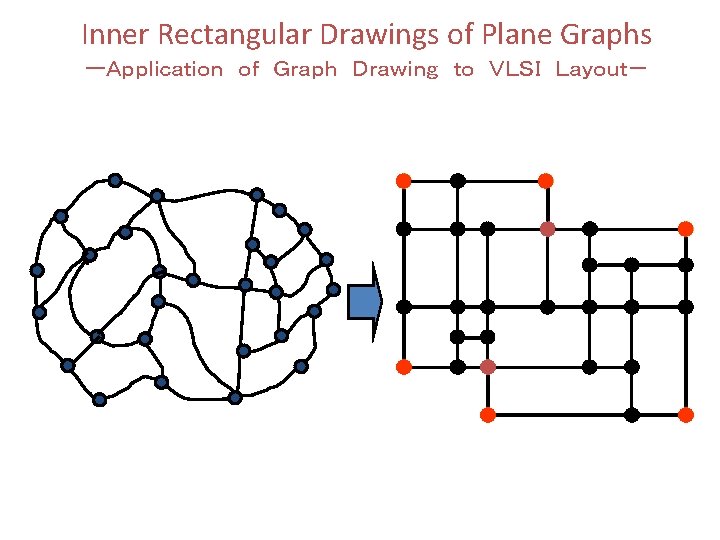
Construct a decision graph Gd Labels of some of the inner angles of G can be immediately determined 2 3 3 1 1 2 2 3 2 2 2 3 1 3 3 2 a plane graph G 3 1 3 2 3

Construct a decision graph Gd 2 3 3 3 1 2 2 3 2 2 2 3 1 3 3 2 a plane graph G 3 1 3 2 3

Construct a decision graph Gd 2 3 3 3 1 2 2 2 3 1 3 3 2 a plane graph G 3 1 3 2 3

Construct a decision graph Gd 2 3 3 3 1 2 2 2 1 1 3 2 1 1 2 2 3 3 2 2 1 1 2 2 3 1 3 3 2 a plane graph G 3 1 3 2 3

Construct a decision graph Gd 2 3 3 3 1 2 2 2 1 1 3 1 1 2 2 3 2 1 1 3 1 3 2 2 3 1 3 3 2 a plane graph G 3 2 3

Construct a decision graph Gd 2 3 3 1 1 2 2 2 1 1 3 1 1 2 3 1 1 1 2 1 1 3 1 3 2 2 3 1 3 3 2 a plane graph G 3 2 3

Construct a decision graph Gd 2 3 3 1 1 2 2 2 1 1 3 1 1 2 3 1 1 1 2 1 1 3 1 3 2 2 3 1 3 3 2 a plane graph G 3 2 3

Construct a decision graph Gd 3 2 1 1 2 2 2 3 11 11 2 2 3 2 11 11 3 2 2 3 1 3 3 2 a plane graph G 3 2 3

Construct a decision graph Gd 3 2 2 1 3 1 1 1 1 2 2 2 3 11 11 2 2 2 3 2 11 11 3 2 2 3 1 3 3 2 a plane graph G 3 2 3

Construct a decision graph Gd 3 2 2 1 1 2 3 1 1 2 2 11 11 2 1 1 3 3 2 a plane graph G 3 1 1 2 2 11 11 2 2 1 1 2 1 3 2 2 3 1 3 2 1 3 1 1 2 3

Construct a decision graph Gd outer vertex of degree 3 2 2 3 1 1 1 1 2 2 11 11 2 3 1 1 2 1 3 1 1 2 a plane graph G 3 3 1 1 1 2 2 1 11 11 2 2 1 1 3 2 2 3 3 1 2 1 3 1 1 2 3

Construct a decision graph Gd 2 2 3 1 1 1 1 2 2 11 11 2 3 1 2 1 3 1 1 2 a plane graph G 3 3 1 1 1 2 2 1 1 11 11 2 2 1 1 3 2 2 3 3 1 2 1 3 1 1 2 3

Construct a decision graph Gd 2 2 3 1 1 2 1 1 1 3 1 1 2 2 1 1 2 1 3 1 1 2 a plane graph G 2 2 3 11 11 1 2 3 1 3 2 2 3 1 1 1 2 2 1 1 11 11 3 1 1 1 2 1 3

Construct a decision graph Gd 2 2 3 1 1 1 1 2 2 11 11 1 21 3 1 1 2 1 3 1 1 2 a plane graph G 2 2 3 1 3 2 2 3 1 1 1 2 2 1 1 11 11 3 1 1 1 2 1 3

Construct a decision graph Gd 2 2 3 2 1 1 21 3 3 1 1 1 2 2 11 11 1 a plane graph G 1 1 2 1 1 3 1 1 2 1 11 1 3 2 2 2 3 1 3 3 1 1 1 2 2 2 1 11 3 1 1 2 1 1 3 1 1 1 2 1 3

Construct a decision graph Gd 2 2 3 2 1 1 21 3 3 1 1 1 2 2 11 11 1 1 2 1 1 1 3 2 a plane graph G 2 2 3 1 1 2 1 1 3 1 1 2 1 3 3 1 1 1 2 2 2 1 11 3 1 1 2 1 1 3 1 1 1 2 1 3

Construct a decision graph Gd 2 2 3 2 1 1 21 3 3 1 1 1 2 2 11 11 1 1 2 1 1 1 3 2 a plane graph G 2 2 3 1 1 2 1 1 3 1 1 2 1 3 3 1 1 1 2 2 2 1 11 1 3 3 1 1 2 1 3

Routing • Connect the various standard cells using wires • Input: – Cell locations, netlist • Output: – Geometric layout of each net connecting various standard cells • Two-step process – Global routing – Detailed routing 88

Global routing 1. In global routing, connections are completed between proper blocks of the circuit disregarding exact geometric details of each wire and pin. 2. For each wire GR finds a lists of channels which are to be used as a passageways for that wire. In other words, GR specifies different regions in the routing space through which a wire should be routed.

Detailed routing • DR completes point-to-point connections between pins on the blocks. • GR is converted into exact routing by specifying geometric information such as location and spacing of wires and their layer assignments. • It includes channel and switchbox routing.

Global routing vs detailed routing* 91 * Sung Kyu Lim

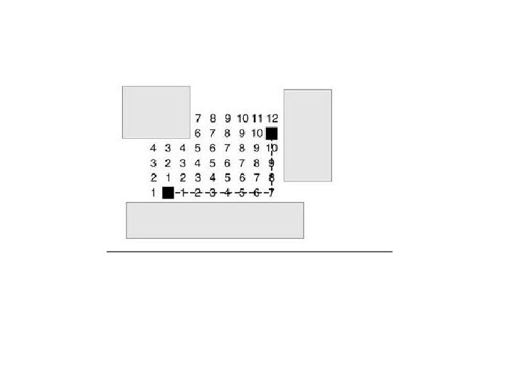
Net Ordering in Area Routing Effect of net ordering on routability A B A´ B´ B´ Optimal routing of net B Optimal routing of net A Nets A and B can be routed only with detours © 2011 Springer Verlag A´ A B 92

Net Ordering in Area Routing Effect of net ordering on total wirelength A A B B A´ Routing net A first A´ Routing net B first © 2011 Springer Verlag B´ B´ 93
 method for finding a short route. • Works")
Line probe routing • Heuristic(experience based) method for finding a short route. • Works with arbitrary combination of obstacles. • Does not explore all possible paths—not optimal.

Line probe example line 1 A A line 2

Maze algorithm • find the shortest path for a single wire between a set of points, if any path exists. • Maze runner is a connection routing method that represents the entire routing space as a grid. • Parts of this grid are blocked by components, specialised areas, or already present wiring. • The grid size corresponds to the wiring pitch of the area. • The goal is to find a chain of grid cells that go from point A to point B.

• Initialisation • Select start point, mark with 0 - i : = 0 • REPEAT - Mark all unlabeled neighbors of points marked with i+1 - i : = i+1 UNTIL ((target reached) or (no points can be marked)) • go to the target point REPEAT - go to next node that has a lower mark than the actual node - add this node to path UNTIL (start point reached) • Block the path for future wirings - Delete all marks

Maze Search 2 2 2 3 3 3 2 2 2 3 2 1 1 1 2 1 S 1 2 3 2 1 S 1 2 1 1 1 2 3 2 1 1 1 2 2 2 3 3 1 T Expansion (1) 1 T Expansion (2) 3 T Backtracing © 2011 Springer Verlag 2 3 98

Maze Search S T 99

Maze routing • Mainly for single-layer routing • Strengths – Finds a connection between two terminals if it exists • Weakness – Large memory required as dense layout – Slow • Application – global routing, detailed routing 101

Routing algorithms • Global routing – Maze routing – Cong/Prea’s algorithm – Spanning tree algorithm – Steiner tree algorithm • Detailed routing – 2 -L Channel routing: Basic left-edge algorithm – Y-K algorithm 102

Specialized routing 103

Power routing 104

Cadence • Virtuoso Layout Suite • Provides the complete physical layout environment of the industrystandard Virtuoso custom design platform, a comprehensive solution for front-to-back custom-analog, digital, RF, and mixedsignal design. • Virtuoso Chip Assembly Router • Performs automated and interactive block and chip authoring for custom-digital, mixed-signal, and analog designs—at any level of the hierarchy. • Cadence Space-Based Router • Offers the performance and capacity to handle designs with growing complexity and increasing digital and analog/mixed-signal content.
- Slides: 105