Power and Performance Optimization of Static CMOS Circuits




![Techniques to Eliminate Glitches ? path delay difference < gate inertial delay [1] path Techniques to Eliminate Glitches ? path delay difference < gate inertial delay [1] path](https://slidetodoc.com/presentation_image_h2/3510c79da1264fe4a6e4dbc5d5f340e9/image-10.jpg)



![Statistical Delay Modeling Deterministic Statistical – normal distribution [ref] Let Mean Xi is a Statistical Delay Modeling Deterministic Statistical – normal distribution [ref] Let Mean Xi is a](https://slidetodoc.com/presentation_image_h2/3510c79da1264fe4a6e4dbc5d5f340e9/image-28.jpg)




- Slides: 49

Power and Performance Optimization of Static CMOS Circuits with Process Variation Yuanlin Lu Department of ECE, Auburn University, Auburn, AL 36849 Ph. D. Dissertation Committee: Dr. Vishwani D. Agrawal Dr. Fa Foster Dai Dr. Charles Stroud Dr. Douglas Leonard (Outsider Reader) May 25, 2007

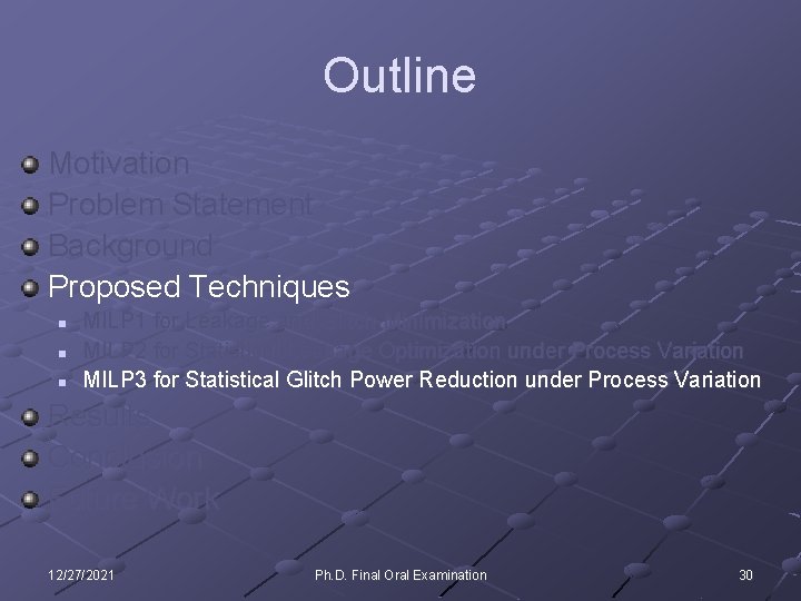
Outline Motivation Problem Statement Background Proposed Techniques n n n MILP 1 for Leakage and Glitch Minimization MILP 2 for Statistical Leakage Optimization under Process Variation MILP 3 for Statistical Glitch Power Reduction under Process Variation Results Conclusion Suggestions for Future Work 12/27/2021 Ph. D. Final Oral Examination 2

Motivation Leakage power has become a dominant contributor to the total power consumption n 65 nm, leakage is ~ 50% of total power consumption Glitches consume 20%-70% of dynamic power Variation of process parameters increases with technology scaling n both average and standard deviation of leakage power increase n some glitch elimination technique (path balancing) is not effective n both power yield and timing yield are degraded 12/27/2021 Ph. D. Final Oral Examination 3

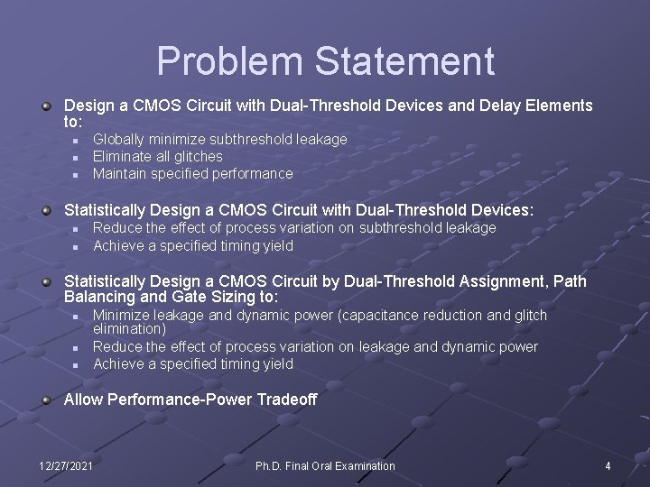
Problem Statement Design a CMOS Circuit with Dual-Threshold Devices and Delay Elements to: n n n Globally minimize subthreshold leakage Eliminate all glitches Maintain specified performance Statistically Design a CMOS Circuit with Dual-Threshold Devices: n n Reduce the effect of process variation on subthreshold leakage Achieve a specified timing yield Statistically Design a CMOS Circuit by Dual-Threshold Assignment, Path Balancing and Gate Sizing to: n n n Minimize leakage and dynamic power (capacitance reduction and glitch elimination) Reduce the effect of process variation on leakage and dynamic power Achieve a specified timing yield Allow Performance-Power Tradeoff 12/27/2021 Ph. D. Final Oral Examination 4

Outline Motivation Problem Statement Background Proposed Techniques Results Conclusion Future Work 12/27/2021 Ph. D. Final Oral Examination 5

Power Consumption in CMOS Circuit CL Dynamic Switching Power + Short Circuit Power + Subthreshold Leakage Power + Gate Leakage Power 12/27/2021 Ph. D. Final Oral Examination 6

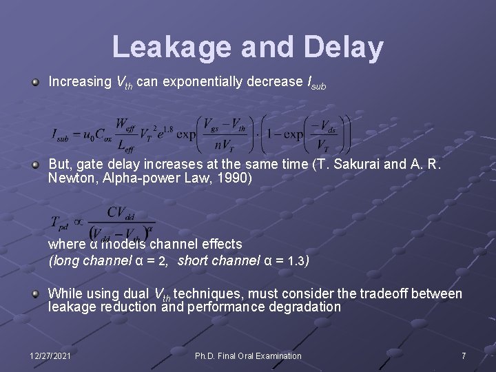
Leakage and Delay Increasing Vth can exponentially decrease Isub But, gate delay increases at the same time (T. Sakurai and A. R. Newton, Alpha-power Law, 1990) where α models channel effects (long channel α = 2, short channel α = 1. 3) While using dual Vth techniques, must consider the tradeoff between leakage reduction and performance degradation 12/27/2021 Ph. D. Final Oral Examination 7

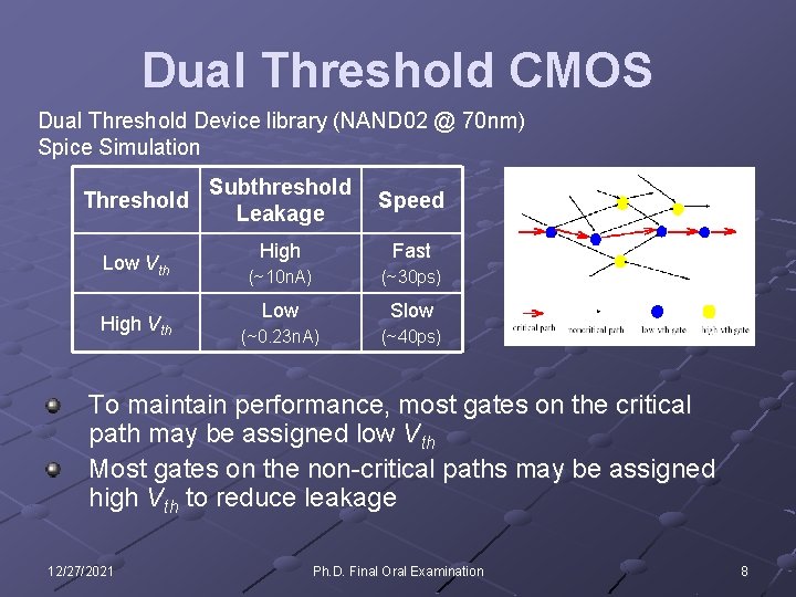
Dual Threshold CMOS Dual Threshold Device library (NAND 02 @ 70 nm) Spice Simulation Threshold Low Vth High Vth Subthreshold Leakage Speed High Fast (~10 n. A) (~30 ps) Low Slow (~0. 23 n. A) (~40 ps) To maintain performance, most gates on the critical path may be assigned low Vth Most gates on the non-critical paths may be assigned high Vth to reduce leakage 12/27/2021 Ph. D. Final Oral Examination 8

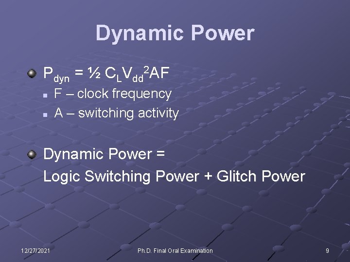
Dynamic Power Pdyn = ½ CLVdd 2 AF n n F – clock frequency A – switching activity Dynamic Power = Logic Switching Power + Glitch Power 12/27/2021 Ph. D. Final Oral Examination 9
![Techniques to Eliminate Glitches path delay difference gate inertial delay 1 path Techniques to Eliminate Glitches ? path delay difference < gate inertial delay [1] path](https://slidetodoc.com/presentation_image_h2/3510c79da1264fe4a6e4dbc5d5f340e9/image-10.jpg)
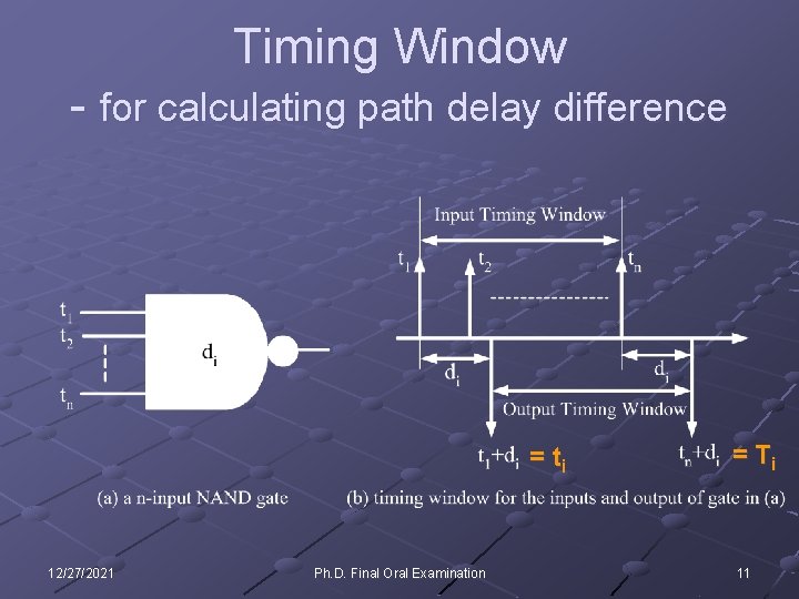
Techniques to Eliminate Glitches ? path delay difference < gate inertial delay [1] path delay difference < gate inertial delay Hazard Filtering (Gate/Transistor Sizing) n n Increase gate inertial delay Sizing gate to change gate delay Path Balancing n n 1→ 3 2 2 1. 5 Decrease path delay difference Insert delay elements on the shorter delay signal path 1 2 2 → 0. 5 [1] V. D. Agrawal, International Conference on VLSI Design, 1997 12/27/2021 Ph. D. Final Oral Examination 10

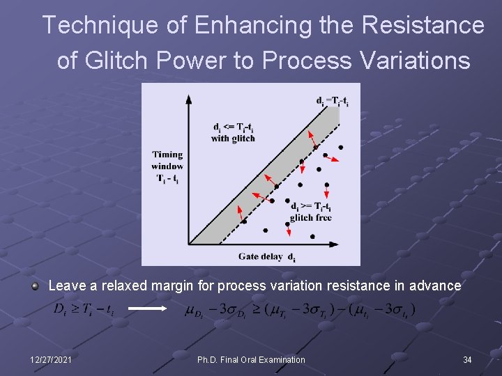
Timing Window - for calculating path delay difference = ti 12/27/2021 Ph. D. Final Oral Examination = Ti 11

Previous Work on Leakage Minimization and Glitch Power Reduction Leakage Power Minimization by Dual-Vth CMOS Devices n Heuristic Algorithms (locally optimum solutions) Q. Wang and S. B. K. Vrudhula, "Static Power Optimization of Deep Submicron CMOS Circuits for Dual VT Technology, " Proc. ICCAD, 1998, pp. 490 -496. L. Wei, Z. Chen, M. Johnson and K. Roy, “Design and Optimization of Low Voltage High Performance Dual Threshold CMOS Circuits, ” Proc. DAC, 1998, pp. 489 -494. n Integer Linear Programming (globally optimum solutions) D. Nguyen, A. Davare, M. Orshansky, D. Chinney, B. Thompson and K. Keutzer, “Minimization of Dynamic and Static Power Through Joint Assignment of Threshold Voltages and Sizing Optimization, ” Proc. ISLPED, 2003, pp. 158 -163. F. Gao and J. P. Hayes, “Gate Sizing and Vt Assignment for Active-Mode Leakage Power Reduction, ” Proc. ICCD, 2004, pp. 258 -264 Glitch Power Elimination by Linear Programming T. Raja, V. D. Agrawal and M. L. Bushnell, “Minimum Dynamic Power CMOS Circuit Design by a Reduced Constraint Set Linear Program, ” Proc. 16 th International Conference on VLSI Design, 2003, pp. 527 -532. 12/27/2021 Ph. D. Final Oral Examination 12

Outline Motivation Problem Statement Background Proposed Techniques n n n MILP 1 for Leakage and Glitch Minimization MILP 2 for Statistical Leakage Optimization under Process Variation MILP 3 for Statistical Glitch Power Reduction under Process Variation Results Conclusion Future Work 12/27/2021 Ph. D. Final Oral Examination 13

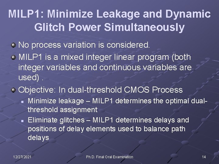
MILP 1: Minimize Leakage and Dynamic Glitch Power Simultaneously No process variation is considered. MILP 1 is a mixed integer linear program (both integer variables and continuous variables are used). Objective: In dual-threshold CMOS Process n n Minimize leakage – MILP 1 determines the optimal dualthreshold assignment Eliminate glitches – MILP 1 determines delays and positions of delay elements used to balance path delays 12/27/2021 Ph. D. Final Oral Examination 14

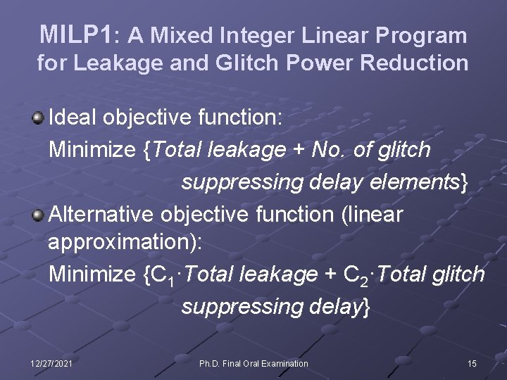
MILP 1: A Mixed Integer Linear Program for Leakage and Glitch Power Reduction Ideal objective function: Minimize {Total leakage + No. of glitch suppressing delay elements} Alternative objective function (linear approximation): Minimize {C 1·Total leakage + C 2·Total glitch suppressing delay} 12/27/2021 Ph. D. Final Oral Examination 15

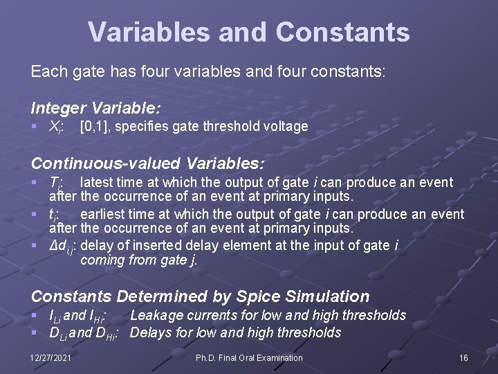
Variables and Constants Each gate has four variables and four constants: Integer Variable: § Xi: [0, 1], specifies gate threshold voltage Continuous-valued Variables: § Ti: latest time at which the output of gate i can produce an event after the occurrence of an event at primary inputs. § ti: earliest time at which the output of gate i can produce an event after the occurrence of an event at primary inputs. § Δdi, j: delay of inserted delay element at the input of gate i coming from gate j. Constants Determined by Spice Simulation § ILi and IHi: Leakage currents for low and high thresholds § DLi and DHi: Delays for low and high thresholds 12/27/2021 Ph. D. Final Oral Examination 16

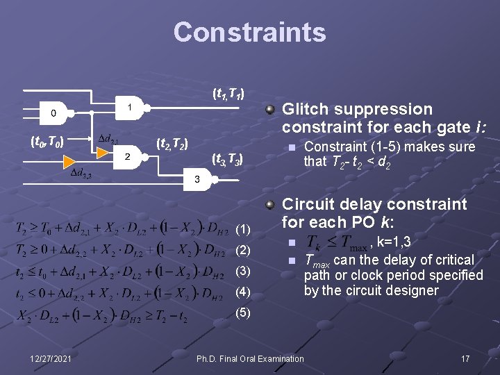
Constraints (t 1, T 1) (t 0, T 0) (t 2, T 2) (t 3, T 3) (1) (2) (3) (4) Glitch suppression constraint for each gate i: n Constraint (1 -5) makes sure that T 2 - t 2 < d 2 Circuit delay constraint for each PO k: , k=1, 3 n Tmax can the delay of critical path or clock period specified by the circuit designer n (5) 12/27/2021 Ph. D. Final Oral Examination 17

Choices for a Delay Element § Two cascaded-inverter buffer - consumes additional short -circuit, subthreshold leakage and dynamic power. § All delay buffers lie on non-critical paths and are assigned high Vth; contribute little to leakage § But they add to dynamic power § Transmission gate (always on) – increases resistance § § Smaller area overhead No subthreshold leakage Minimal capacitance increase Used before § T. Raja, V. D. Agrawal and M. L. Bushnell, “Variable Input Delay CMOS Logic for Low Power Design, ” Proc. 18 th International Conference on VLSI Design, January 2005, pp. 598 -605. § T. Raja, V. D. Agrawal and M. L. Bushnell, “Transistor Sizing of Logic Gates to Maximize Input Delay Variability, ” JOLPE, vol. 2, no. 1, pp. 121 -128, April 2006. 12/27/2021 Ph. D. Final Oral Examination 18

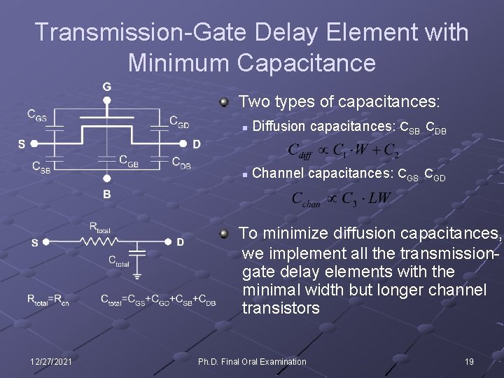
Transmission-Gate Delay Element with Minimum Capacitance Two types of capacitances: n Diffusion capacitances: CSB CDB n Channel capacitances: CGS CGD To minimize diffusion capacitances, we implement all the transmissiongate delay elements with the minimal width but longer channel transistors 12/27/2021 Ph. D. Final Oral Examination 19

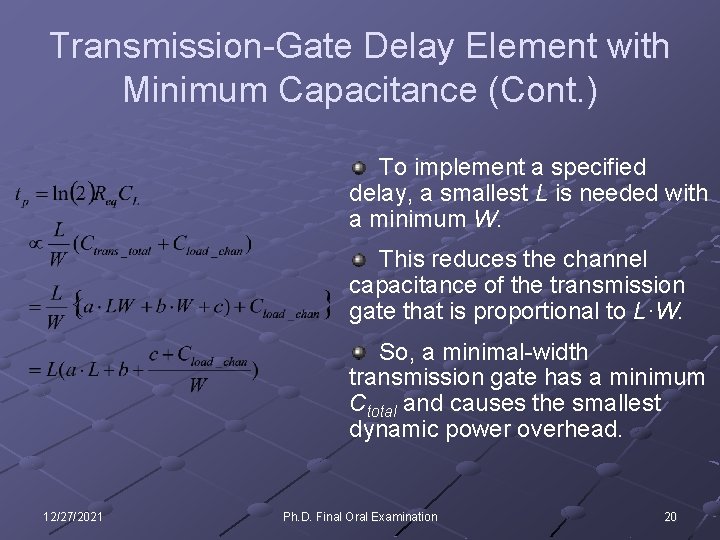
Transmission-Gate Delay Element with Minimum Capacitance (Cont. ) To implement a specified delay, a smallest L is needed with a minimum W. This reduces the channel capacitance of the transmission gate that is proportional to L·W. So, a minimal-width transmission gate has a minimum Ctotal and causes the smallest dynamic power overhead. 12/27/2021 Ph. D. Final Oral Examination 20

Outline Motivation Problem Statement Background Proposed Techniques n n n MILP 1 for Leakage and Glitch Minimization MILP 2 for Statistical Leakage Optimization under Process Variation MILP 3 for Statistical Glitch Power Reduction under Process Variation Results Conclusion Future Work 12/27/2021 Ph. D. Final Oral Examination 21

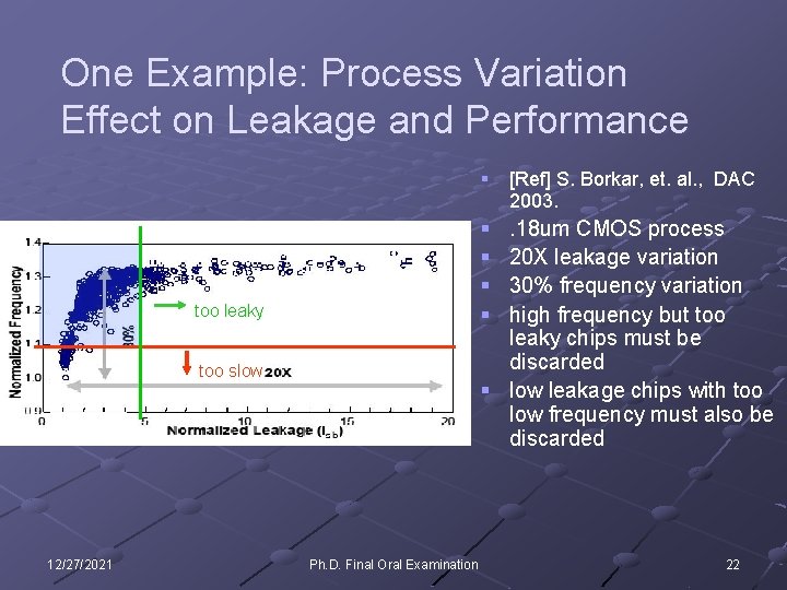
One Example: Process Variation Effect on Leakage and Performance § § § . 18 um CMOS process 20 X leakage variation 30% frequency variation high frequency but too leaky chips must be discarded § low leakage chips with too low frequency must also be discarded too leaky too slow 12/27/2021 [Ref] S. Borkar, et. al. , DAC 2003. Ph. D. Final Oral Examination 22

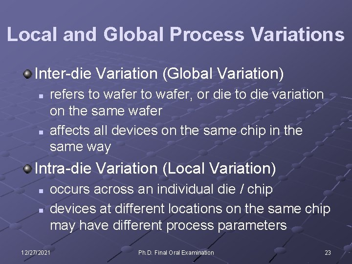
Local and Global Process Variations Inter-die Variation (Global Variation) n n refers to wafer, or die to die variation on the same wafer affects all devices on the same chip in the same way Intra-die Variation (Local Variation) n n occurs across an individual die / chip devices at different locations on the same chip may have different process parameters 12/27/2021 Ph. D. Final Oral Examination 23

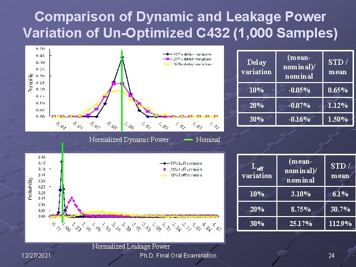
Comparison of Dynamic and Leakage Power Variation of Un-Optimized C 432 (1, 000 Samples) Normalized Dynamic Power Delay variation (meannominal)/ nominal STD / mean 10% -0. 05% 0. 65% 20% -0. 07% 1. 12% 30% -0. 16% 1. 50% Leff variation (meannominal)/ nominal STD / mean 10% 3. 10% 6. 1% 20% 8. 75% 30. 7% 30% 25. 17% 112. 9% Nominal Normalized Leakage Power 12/27/2021 Ph. D. Final Oral Examination 24

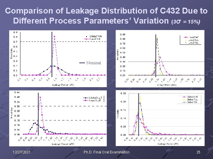
Comparison of Leakage Distribution of C 432 Due to Different Process Parameters’ Variation (3σ = 15%) Nominal 12/27/2021 Ph. D. Final Oral Examination 25

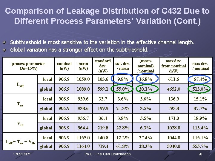
Comparison of Leakage Distribution of C 432 Due to Different Process Parameters’ Variation (Cont. ) Subthreshold is most sensitive to the variation in the effective channel length. Global variation has a stronger effect on the subthreshold. nominal (n. W) mean (n. W) standard dev. (n. W) std. dev. / mean (meannominal) / nominal max dev. from nominal (n. W) max dev. / nominal local 906. 9 1059. 0 103. 6 9. 8% 16. 8% 611. 6 67. 4% global 906. 9 1089. 0 599. 1 55. 0% 20. 1% 4652. 0 513. 0% local 906. 9 939. 6 33. 7 3. 6% 136. 9 15. 1% global 906. 9 938. 6 199. 9 21. 3% 3. 5% 795. 8 87. 7% local 906. 9 956. 7 36. 4 3. 8% 5. 5% 171. 0 18. 9% global 906. 9 964. 4 219. 8 22. 8% 6. 3% 1028. 0 113. 4% local 906. 9 1155. 0 140. 8 12. 2% 27. 4% 1044. 0 115. 1% global 906. 9 1164. 0 719. 4 61. 8% 28. 3% 5040. 0 555. 7% process parameter (3σ=15%) Leff Tox Vth Leff + Tox + Vth 12/27/2021 Ph. D. Final Oral Examination 26

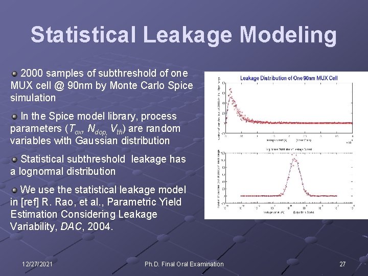
Statistical Leakage Modeling 2000 samples of subthreshold of one MUX cell @ 90 nm by Monte Carlo Spice simulation In the Spice model library, process parameters (Tox, Ndop, Vth) are random variables with Gaussian distribution Statistical subthreshold leakage has a lognormal distribution We use the statistical leakage model in [ref] R. Rao, et al. , Parametric Yield Estimation Considering Leakage Variability, DAC, 2004. 12/27/2021 Ph. D. Final Oral Examination 27
![Statistical Delay Modeling Deterministic Statistical normal distribution ref Let Mean Xi is a Statistical Delay Modeling Deterministic Statistical – normal distribution [ref] Let Mean Xi is a](https://slidetodoc.com/presentation_image_h2/3510c79da1264fe4a6e4dbc5d5f340e9/image-28.jpg)
Statistical Delay Modeling Deterministic Statistical – normal distribution [ref] Let Mean Xi is a process parameter, Xi 0 is the nominal value of Xi Standard Deviation Let {X 1, X 2, X 3} = {Leff, Tox, Ndop} [ref] A. Davoodi and A. Srivastava, ISLPED, 2005. 12/27/2021 Ph. D. Final Oral Examination 28

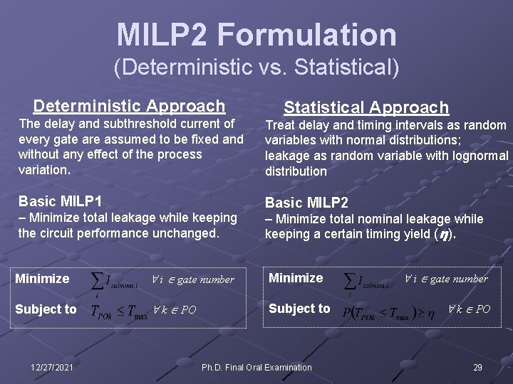
MILP 2 Formulation (Deterministic vs. Statistical) Deterministic Approach Statistical Approach The delay and subthreshold current of every gate are assumed to be fixed and without any effect of the process variation. Treat delay and timing intervals as random variables with normal distributions; leakage as random variable with lognormal distribution Basic MILP 1 Basic MILP 2 – Minimize total leakage while keeping the circuit performance unchanged. – Minimize total nominal leakage while keeping a certain timing yield (η). Minimize " i Î gate number Minimize Subject to " k Î PO Subject to 12/27/2021 Ph. D. Final Oral Examination " i Î gate number " k Î PO 29

Outline Motivation Problem Statement Background Proposed Techniques n n n MILP 1 for Leakage and Glitch Minimization MILP 2 for Statistical Leakage Optimization under Process Variation MILP 3 for Statistical Glitch Power Reduction under Process Variation Results Conclusion Future Work 12/27/2021 Ph. D. Final Oral Examination 30

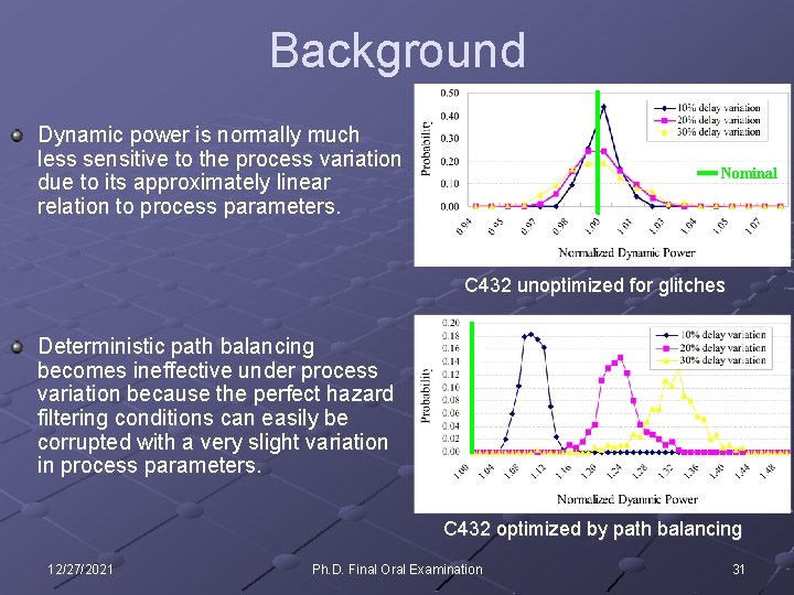
Background Dynamic power is normally much less sensitive to the process variation due to its approximately linear relation to process parameters. Nominal C 432 unoptimized for glitches Deterministic path balancing becomes ineffective under process variation because the perfect hazard filtering conditions can easily be corrupted with a very slight variation in process parameters. C 432 optimized by path balancing 12/27/2021 Ph. D. Final Oral Examination 31

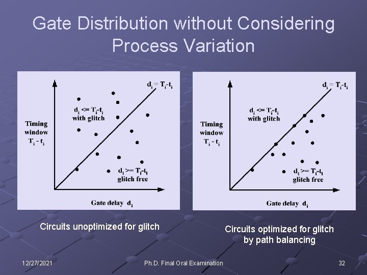
Gate Distribution without Considering Process Variation Circuits unoptimized for glitch 12/27/2021 Ph. D. Final Oral Examination Circuits optimized for glitch by path balancing 32

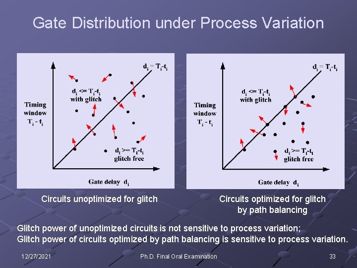
Gate Distribution under Process Variation Circuits unoptimized for glitch Circuits optimized for glitch by path balancing Glitch power of unoptimized circuits is not sensitive to process variation; Glitch power of circuits optimized by path balancing is sensitive to process variation. 12/27/2021 Ph. D. Final Oral Examination 33

Technique of Enhancing the Resistance of Glitch Power to Process Variations Leave a relaxed margin for process variation resistance in advance 12/27/2021 Ph. D. Final Oral Examination 34

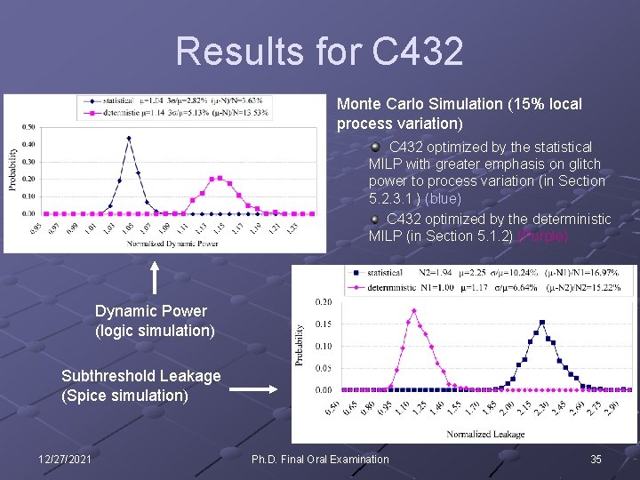
Results for C 432 Monte Carlo Simulation (15% local process variation) C 432 optimized by the statistical MILP with greater emphasis on glitch power to process variation (in Section 5. 2. 3. 1 ) (blue) C 432 optimized by the deterministic MILP (in Section 5. 1. 2) (Purple) Dynamic Power (logic simulation) Subthreshold Leakage (Spice simulation) 12/27/2021 Ph. D. Final Oral Examination 35

Outline Motivation Problem Statement Background Proposed Techniques Results Conclusion Future Work 12/27/2021 Ph. D. Final Oral Examination 36

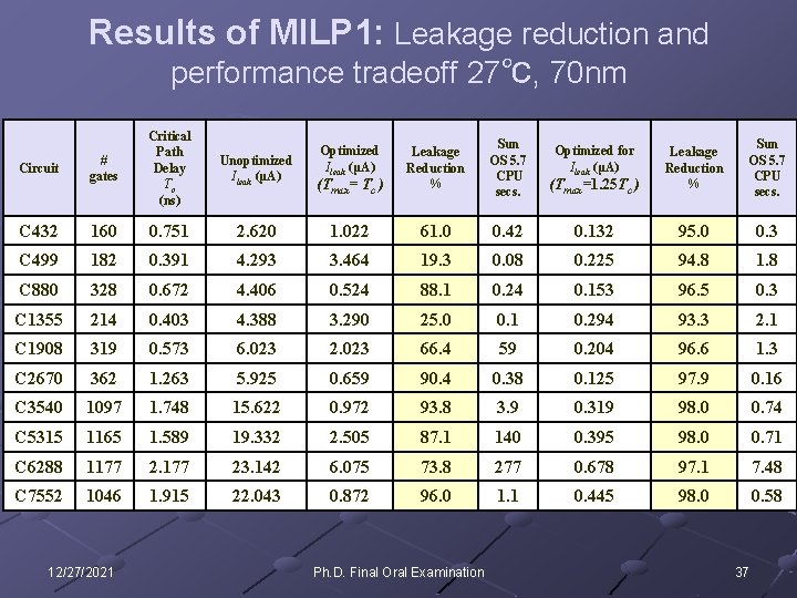
Results of MILP 1: Leakage reduction and performance tradeoff 27℃, 70 nm # gates Critical Path Delay Tc (ns) Unoptimized Ileak (μA) C 432 160 0. 751 C 499 182 C 880 Optimized Ileak (μA) (Tmax= Tc ) Leakage Reduction % Sun OS 5. 7 CPU secs. Optimized for Ileak (μA) (Tmax=1. 25 Tc ) Leakage Reduction % Sun OS 5. 7 CPU secs. 2. 620 1. 022 61. 0 0. 42 0. 132 95. 0 0. 391 4. 293 3. 464 19. 3 0. 08 0. 225 94. 8 1. 8 328 0. 672 4. 406 0. 524 88. 1 0. 24 0. 153 96. 5 0. 3 C 1355 214 0. 403 4. 388 3. 290 25. 0 0. 1 0. 294 93. 3 2. 1 C 1908 319 0. 573 6. 023 2. 023 66. 4 59 0. 204 96. 6 1. 3 C 2670 362 1. 263 5. 925 0. 659 90. 4 0. 38 0. 125 97. 9 0. 16 C 3540 1097 1. 748 15. 622 0. 972 93. 8 3. 9 0. 319 98. 0 0. 74 C 5315 1165 1. 589 19. 332 2. 505 87. 1 140 0. 395 98. 0 0. 71 C 6288 1177 23. 142 6. 075 73. 8 277 0. 678 97. 1 7. 48 C 7552 1046 1. 915 22. 043 0. 872 96. 0 1. 1 0. 445 98. 0 0. 58 Circuit 12/27/2021 Ph. D. Final Oral Examination 37

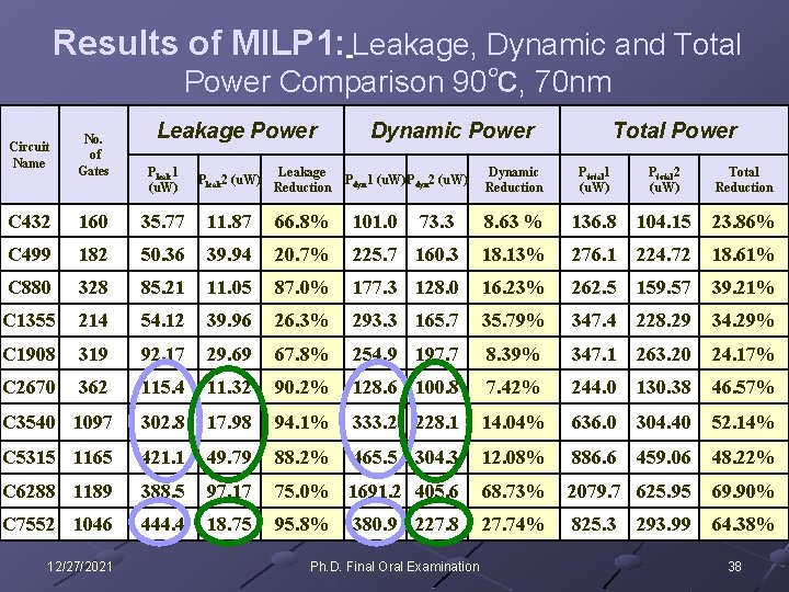
Results of MILP 1: Leakage, Dynamic and Total Power Comparison 90℃, 70 nm Circuit Name No. of Gates Leakage Power Pleak 1 (u. W) Pleak 2 (u. W) Leakage Reduction Dynamic Power Pdyn 1 (u. W)Pdyn 2 (u. W) Total Power Dynamic Reduction Ptotal 1 (u. W) Ptotal 2 (u. W) Total Reduction C 432 160 35. 77 11. 87 66. 8% 101. 0 73. 3 8. 63 % 136. 8 104. 15 23. 86% C 499 182 50. 36 39. 94 20. 7% 225. 7 160. 3 18. 13% 276. 1 224. 72 18. 61% C 880 328 85. 21 11. 05 87. 0% 177. 3 128. 0 16. 23% 262. 5 159. 57 39. 21% C 1355 214 54. 12 39. 96 26. 3% 293. 3 165. 7 35. 79% 347. 4 228. 29 34. 29% C 1908 319 92. 17 29. 69 67. 8% 254. 9 197. 7 8. 39% 347. 1 263. 20 24. 17% C 2670 362 115. 4 11. 32 90. 2% 128. 6 100. 8 7. 42% 244. 0 130. 38 46. 57% C 3540 1097 302. 8 17. 98 94. 1% 333. 2 228. 1 14. 04% 636. 0 304. 40 52. 14% C 5315 1165 421. 1 49. 79 88. 2% 465. 5 304. 3 12. 08% 886. 6 459. 06 48. 22% C 6288 1189 388. 5 97. 17 75. 0% 1691. 2 405. 6 68. 73% 2079. 7 625. 95 69. 90% C 7552 1046 444. 4 18. 75 95. 8% 27. 74% 825. 3 64. 38% 12/27/2021 380. 9 227. 8 Ph. D. Final Oral Examination 293. 99 38

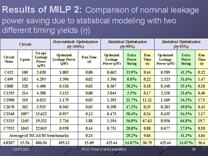
Results of MILP 2: Comparison of nominal leakage power saving due to statistical modeling with two different timing yields (η). Deterministic Optimization (η=100%) Circuit Statistical Optimization (η=99%) Statistical Optimization (η=95%) Circuit Name # gates Un-opt. Leakage Power (μW) C 432 160 2. 620 1. 003 0. 00 0. 662 33. 9% 0. 44 0. 589 41. 3% 0. 32 C 499 182 4. 293 3. 396 0. 02 3. 396 0. 0% 0. 22 2. 323 31. 6% 1. 47 C 880 328 4. 406 0. 526 0. 02 0. 367 30. 2% 0. 18 0. 340 35. 4% 0. 18 C 1355 214 4. 388 3. 153 0. 00 3. 044 3. 5% 0. 17 2. 158 31. 6% 0. 48 C 1908 319 6. 023 1. 179 0. 03 1. 392 21. 7% 11. 21 1. 169 34. 3% 17. 5 C 2670 362 5. 925 0. 565 0. 03 0. 298 47. 2% 0. 35 0. 283 49. 8% 0. 43 C 3540 1097 15. 622 0. 957 0. 13 0. 475 50. 4% 0. 24 0. 435 54. 5% 1. 17 C 5315 1165 19. 332 2. 716 1. 88 1. 194 56. 0% 67. 63 0. 956 64. 8% 19. 7 C 7552 1045 22. 043 0. 938 0. 44 0. 751 20. 0% 0. 88 0. 677 27. 9% 0. 58 Average of ISCAS’ 85 benchmarks 0. 24 29. 2% 9. 04 41. 3% 4. 64 14. 07% 36. 79 14. 07% 36. 4 ARM 7 15. 5 k 12/27/2021 686. 56 Optimized Leakage Power (μW) Run Time (s) Optimized Leakage Power (μW) Extra Power Saving Run Time (s) 495. 12 15. 69 425. 44 Ph. D. Final Oral Examination 425. 44 39

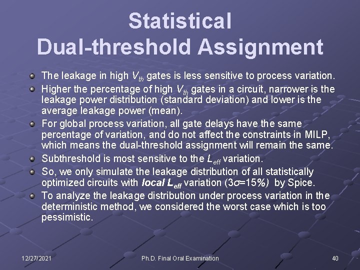
Statistical Dual-threshold Assignment The leakage in high Vth gates is less sensitive to process variation. Higher the percentage of high Vth gates in a circuit, narrower is the leakage power distribution (standard deviation) and lower is the average leakage power (mean). For global process variation, all gate delays have the same percentage of variation, and do not affect the constraints in MILP, which means the dual-threshold assignment will remain the same. Subthreshold is most sensitive to the Leff variation. So, we only simulate the leakage distribution of all statistically optimized circuits with local Leff variation (3σ=15%) by Spice. To analyze the leakage distribution under process variation in the deterministic method, we considered the worst case which is too pessimistic. 12/27/2021 Ph. D. Final Oral Examination 40

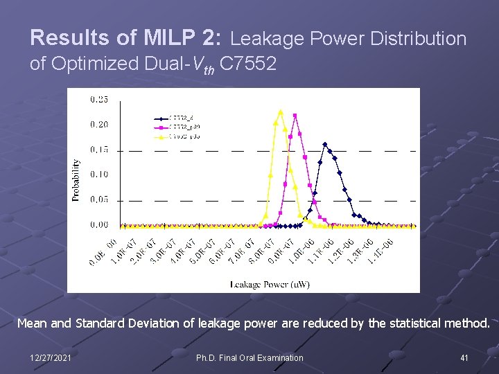
Results of MILP 2: Leakage Power Distribution of Optimized Dual-Vth C 7552 Mean and Standard Deviation of leakage power are reduced by the statistical method. 12/27/2021 Ph. D. Final Oral Examination 41

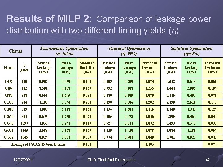
Results of MILP 2: Comparison of leakage power distribution with two different timing yields (η). Circuit Deterministic Optimization (η=100%) Statistical Optimization (η=99%) Statistical Optimization (η=95%) Name # gates Nominal Leakage (u. W) Mean Leakage (u. W) Standard Deviation (uw) Nominal Leakage (u. W) Mean Leakage (u. W) Standard Deviation (u. W) C 432 160 0. 907 1. 059 0. 104 0. 603 0. 709 0. 074 0. 522 0. 614 0. 069 C 499 182 3. 592 4. 283 0. 255 2. 464 2. 905 0. 197 C 880 328 0. 551 0. 645 0. 086 0. 430 0. 509 0. 080 0. 415 0. 491 0. 079 C 1355 214 3. 198 3. 744 0. 200 3. 090 3. 606 0. 202 2. 199 2. 610 0. 175 C 1908 319 1. 803 2. 123 0. 170 1. 356 1. 601 0. 116 1. 140 1. 341 0. 127 C 2670 362 0. 635 0. 750 0. 078 0. 405 0. 473 0. 046 0. 395 0. 461 0. 043 C 3540 1097 1. 055 1. 243 0. 119 0. 527 0. 611 0. 032 0. 493 0. 575 0. 031 C 5315 1165 2. 688 3. 128 0. 165 1. 229 1. 420 0. 088 1. 034 1. 188 0. 067 C 7552 1045 0. 924 1. 073 0. 069 0. 774 0. 903 0. 049 0. 701 0. 823 0. 045 Average of ISCAS’ 85 benchmarks 12/27/2021 0. 138 Ph. D. Final Oral Examination 0. 105 0. 093 42

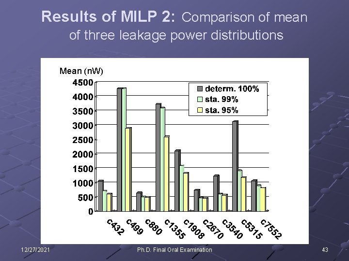
Results of MILP 2: Comparison of mean of three leakage power distributions Mean (n. W) 12/27/2021 Ph. D. Final Oral Examination 43

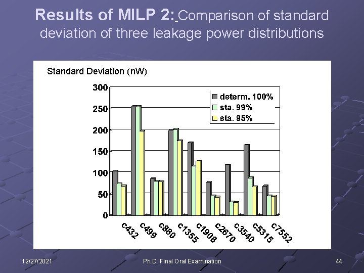
Results of MILP 2: Comparison of standard deviation of three leakage power distributions Standard Deviation (n. W) 12/27/2021 Ph. D. Final Oral Examination 44

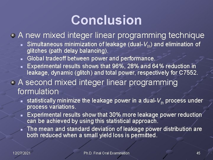
Conclusion A new mixed integer linear programming technique n n n Simultaneous minimization of leakage (dual-Vth) and elimination of glitches (path delay balancing). Global tradeoff between power and performance. Experimental results shows that 96%, 28% and 64% reduction in leakage, dynamic (glitch) and total power, respectively for C 7552. A second mixed integer linear programming formulation n statistically minimize the leakage power in a dual-Vth process under process variations. Experimental results show that 30% more leakage power reduction can be achieved by using this statistical approach. The mean and standard deviation of leakage power distribution are both reduced when a small yield loss is permitted. 12/27/2021 Ph. D. Final Oral Examination 45

Conclusion (cont. ) A third mixed integer linear programming formulation n n Statistically minimize the total power, the leakage or the dynamic power in a dual-Vth process under process variations The effect of process variation on glitch power is minimized. 12/27/2021 Ph. D. Final Oral Examination 46

Future Work Gate leakage MILP complexity n for SOC, MILP constraints can be generated for its submodules at a lower level, may not guarantee a global optimization, but still would get a reasonable result within acceptable run time. n adopt relaxed LP that uses the LP solution as the starting point and then round off the variables An approximate optimal solution with acceptable run time can be achieved. 12/27/2021 Ph. D. Final Oral Examination 47

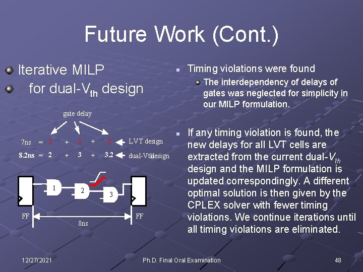
Future Work (Cont. ) Iterative MILP for dual-Vth design n Timing violations were found The interdependency of delays of gates was neglected for simplicity in our MILP formulation. gate delay n = 2 + 3 8. 2 ns = 2 + 3. 2 7 ns 1 FF 12/27/2021 2 8 ns LVT design dual-Vthdesign 3 FF If any timing violation is found, the new delays for all LVT cells are extracted from the current dual-Vth design and the MILP formulation is updated correspondingly. A different optimal solution is then given by the CPLEX solver with fewer timing violations. We continue iterations until all timing violations are eliminated. Ph. D. Final Oral Examination 48

Thank You All ! Questions?