Power and Performance Optimization of CMOS Static Circuits
![Transistor Leakage Mechanisms [1] § § § § I 2, I 5, I 6 Transistor Leakage Mechanisms [1] § § § § I 2, I 5, I 6](https://slidetodoc.com/presentation_image_h2/9dd1c3e5798cd2e196c8ee60cf14a589/image-6.jpg)
![Techniques to Eliminate Glitches ? path delay difference < gate inertial delay [1] path Techniques to Eliminate Glitches ? path delay difference < gate inertial delay [1] path](https://slidetodoc.com/presentation_image_h2/9dd1c3e5798cd2e196c8ee60cf14a589/image-11.jpg)
![Statistical Leakage Modeling Deterministic Statistical – lognormal distribution [ref] Statistical of Total Leakage – Statistical Leakage Modeling Deterministic Statistical – lognormal distribution [ref] Statistical of Total Leakage –](https://slidetodoc.com/presentation_image_h2/9dd1c3e5798cd2e196c8ee60cf14a589/image-33.jpg)
![Statistical Delay Modeling Deterministic Statistical – normal distribution [ref] Let Xi is a process Statistical Delay Modeling Deterministic Statistical – normal distribution [ref] Let Xi is a process](https://slidetodoc.com/presentation_image_h2/9dd1c3e5798cd2e196c8ee60cf14a589/image-34.jpg)

- Slides: 50

Power and Performance Optimization of CMOS Static Circuits with Process Variation Ph. D. General Oral Examination Yuanlin Lu Advisor: Dr. Vishwani D. Agrawal Committee: Dr. Charles Stroud and Dr. Fa Foster Dai ECE Department, Auburn University Dec. 6, 2006 Ph. D. General Oral Examination 1

Outline § § Motivation Problem Statement Background Proposed Techniques Ø MILP 1 for Leakage and Glitch Minimization Ø MILP 2 for Statistical Leakage Optimization under Process Variation Ø Results § Conclusion § Future Work and Timeline Dec. 6, 2006 Ph. D. General Oral Examination 2

Motivation § Leakage power is becoming a dominant contributor to the total power consumption Ø 65 nm, leakage is ~ 50% of total power consumption § Variation of process parameters increases with technology scaling Ø exponential relation between the leakage current and some key process parameters Ø both average and standard deviation of leakage power increase Ø both power yield and timing yield are degraded Dec. 6, 2006 Ph. D. General Oral Examination 3

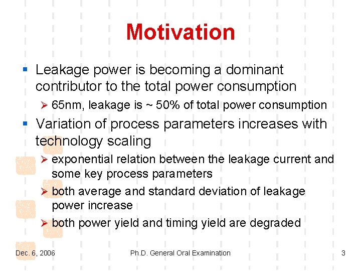
Problem Statement § Design a CMOS Circuit with Dual-Threshold Devices and Delay Elements to: Ø Globally minimize subthreshold leakage Ø Eliminate all glitches Ø Keep specified performance § Statistically Design a CMOS Circuit with Dual. Threshold Devices: Ø Reduce the effect of process variation on subthreshold leakage Ø Achieve a specified timing yield § Allow Performance-Power Tradeoff Dec. 6, 2006 Ph. D. General Oral Examination 4

Outline § § Motivation Problem Statement Background Proposed Techniques Ø MILP 1 for Leakage and Glitch Minimization Ø MILP 2 for Statistical Leakage Optimization under Process Variation Ø Results § Conclusion § Future Work and Timeline Dec. 6, 2006 Ph. D. General Oral Examination 5
![Transistor Leakage Mechanisms 1 I 2 I 5 I 6 Transistor Leakage Mechanisms [1] § § § § I 2, I 5, I 6](https://slidetodoc.com/presentation_image_h2/9dd1c3e5798cd2e196c8ee60cf14a589/image-6.jpg)
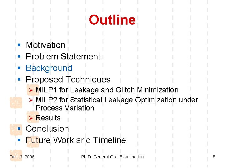
Transistor Leakage Mechanisms [1] § § § § I 2, I 5, I 6 and are off-state leakage mechanisms; I 1 and I 3 occur in both ON and OFF states; I 4 can occur in the off state, but more typically occurs during the transistor bias states in transition. Dec. 6, 2006 I 1 - reverse-biased pn junction leakage; I 2 - subthreshold leakage; weak inversion conduction current between source and drain in an MOS transistor occurs when gate voltage is below Vth. I 3 – gate leakage, the oxide tunneling current; due to the low oxide thickness and the high electric field; I 4 - gate current due to hot-carrier injection; I 5 - GIDL (Gate-Induced Drain Leakage); due to high field effect in the drain junction; I 6 - channel punchthrough current; due to the proximity of the depletion regions of the drain and the source. [1] K. Roy et al, “Leakage Current Mechanisms and Leakage Reduction Techniques in Deep-Sub micrometer CMOS Circuits”, Proceedings of the IEEE, Volume 91, Issue 2, Feb. 2003 pp 305 – 327. Ph. D. General Oral Examination 6

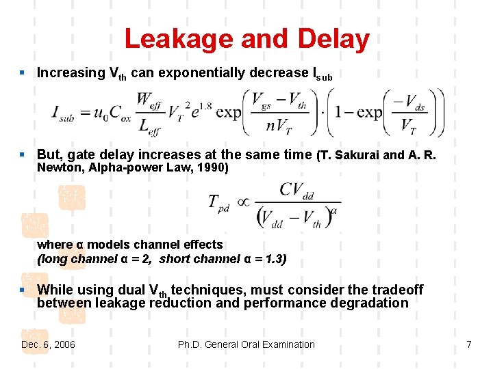
Leakage and Delay § Increasing Vth can exponentially decrease Isub § But, gate delay increases at the same time (T. Sakurai and A. R. Newton, Alpha-power Law, 1990) where α models channel effects (long channel α = 2, short channel α = 1. 3) § While using dual Vth techniques, must consider the tradeoff between leakage reduction and performance degradation Dec. 6, 2006 Ph. D. General Oral Examination 7

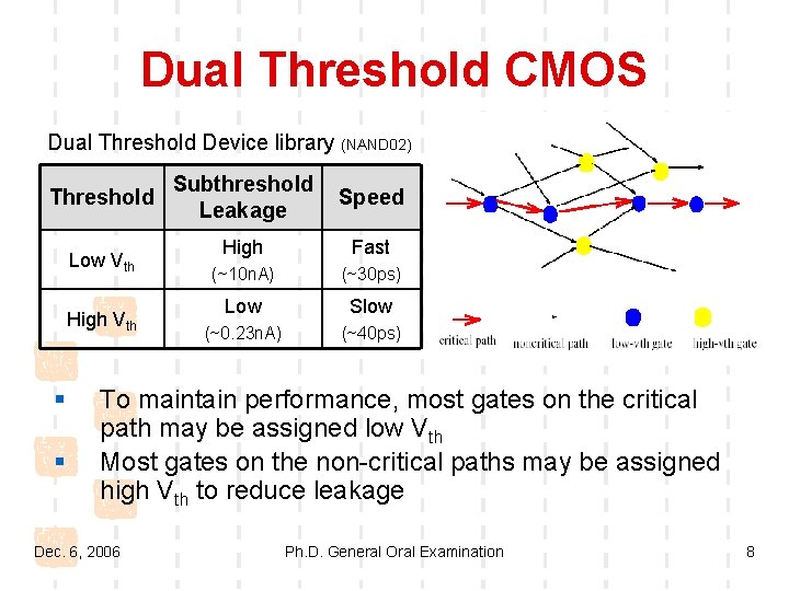
Dual Threshold CMOS Dual Threshold Device library (NAND 02) Threshold Low Vth High Vth § § Subthreshold Leakage Speed High Fast (~10 n. A) (~30 ps) Low Slow (~0. 23 n. A) (~40 ps) To maintain performance, most gates on the critical path may be assigned low Vth Most gates on the non-critical paths may be assigned high Vth to reduce leakage Dec. 6, 2006 Ph. D. General Oral Examination 8

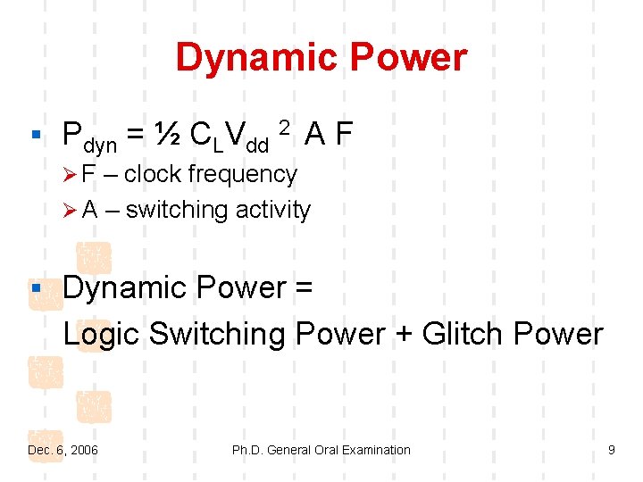
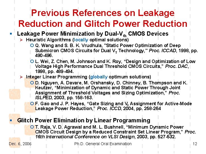
Dynamic Power § Pdyn = ½ CLVdd 2 AF Ø F – clock frequency Ø A – switching activity § Dynamic Power = Logic Switching Power + Glitch Power Dec. 6, 2006 Ph. D. General Oral Examination 9

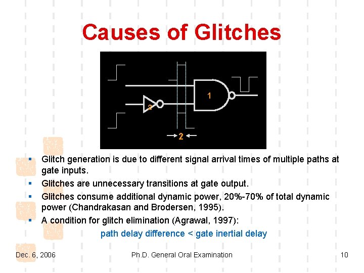
Causes of Glitches 1 2 2 § § Glitch generation is due to different signal arrival times of multiple paths at gate inputs. Glitches are unnecessary transitions at gate output. Glitches consume additional dynamic power, 20%-70% of total dynamic power (Chandrakasan and Brodersen, 1995). A condition for glitch elimination (Agrawal, 1997): path delay difference < gate inertial delay Dec. 6, 2006 Ph. D. General Oral Examination 10
![Techniques to Eliminate Glitches path delay difference gate inertial delay 1 path Techniques to Eliminate Glitches ? path delay difference < gate inertial delay [1] path](https://slidetodoc.com/presentation_image_h2/9dd1c3e5798cd2e196c8ee60cf14a589/image-11.jpg)
Techniques to Eliminate Glitches ? path delay difference < gate inertial delay [1] path delay difference < gate inertial delay § Gate/Transistor Sizing Ø Increase gate inertial delay Ø Gate sizing to change gate delay 1→ 3 2 2 § Path Balancing Ø Decrease path delay difference 1. 5 Ø Insert delay elements on the earlier arrival signal path [1] V. D. Agrawal, International Conference on VLSI Design, 1997 Dec. 6, 2006 Ph. D. General Oral Examination 1 2 2 → 0. 5 11

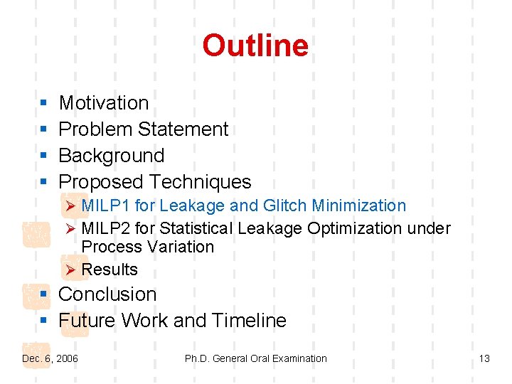
Previous References on Leakage Reduction and Glitch Power Reduction § Leakage Power Minimization by Dual-Vth CMOS Devices Ø Heuristic Algorithms (locally optimal solutions) ¡ Q. Wang and S. B. K. Vrudhula, "Static Power Optimization of Deep Submicron CMOS Circuits for Dual VT Technology, " Proc. ICCAD, 1998, pp. 490 -496. ¡ L. Wei, Z. Chen, M. Johnson and K. Roy, “Design and Optimization of Low Voltage High Performance Dual Threshold CMOS Circuits, ” Proc. DAC, 1998, pp. 489 -494. Ø Integer Linear Programming (globally optimum solutions) ¡ D. Nguyen, A. Davare, M. Orshansky, D. Chinney, B. Thompson and K. Keutzer, “Minimization of Dynamic and Static Power Through Joint Assignment of Threshold Voltages and Sizing Optimization, ” Proc. ISLPED, 2003, pp. 158 -163. ¡ F. Gao and J. P. Hayes, “Gate Sizing and Vt Assignment for Active-Mode Leakage Power Reduction, ” Proc. ICCD, 2004, pp. 258 -264 § Glitch Power Elimination by Linear Programming ¡ T. Raja, V. D. Agrawal and M. L. Bushnell, “Minimum Dynamic Power CMOS Circuit Design by a Reduced Constraint Set Linear Program, ” Proc. 16 th International Conference on VLSI Design, 2003, pp. 527 -532. Dec. 6, 2006 Ph. D. General Oral Examination 12

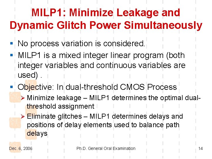
Outline § § Motivation Problem Statement Background Proposed Techniques Ø MILP 1 for Leakage and Glitch Minimization Ø MILP 2 for Statistical Leakage Optimization under Process Variation Ø Results § Conclusion § Future Work and Timeline Dec. 6, 2006 Ph. D. General Oral Examination 13

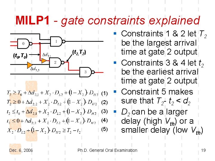
MILP 1: Minimize Leakage and Dynamic Glitch Power Simultaneously § No process variation is considered. § MILP 1 is a mixed integer linear program (both integer variables and continuous variables are used). § Objective: In dual-threshold CMOS Process Ø Minimize leakage – MILP 1 determines the optimal dual- threshold assignment Ø Eliminate glitches – MILP 1 determines delays and positions of delay elements used to balance path delays Dec. 6, 2006 Ph. D. General Oral Examination 14

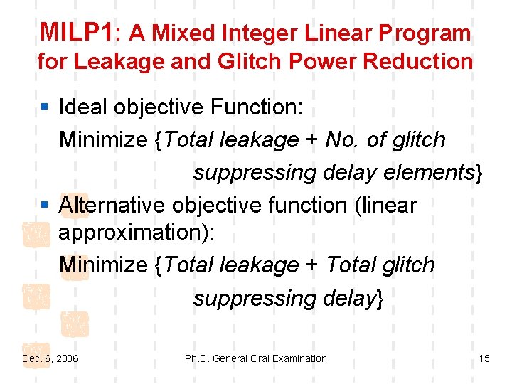
MILP 1: A Mixed Integer Linear Program for Leakage and Glitch Power Reduction § Ideal objective Function: Minimize {Total leakage + No. of glitch suppressing delay elements} § Alternative objective function (linear approximation): Minimize {Total leakage + Total glitch suppressing delay} Dec. 6, 2006 Ph. D. General Oral Examination 15

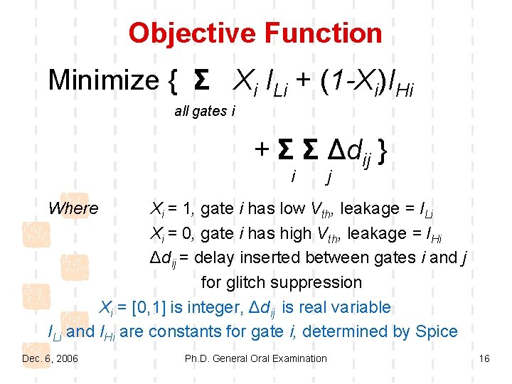
Objective Function Minimize { Σ Xi ILi + (1 -Xi)IHi all gates i + Σ Σ Δdij } i j Where Xi = 1, gate i has low Vth, leakage = ILi Xi = 0, gate i has high Vth, leakage = IHi Δdij = delay inserted between gates i and j for glitch suppression Xi = [0, 1] is integer, Δdij is real variable ILi and IHi are constants for gate i, determined by Spice Dec. 6, 2006 Ph. D. General Oral Examination 16

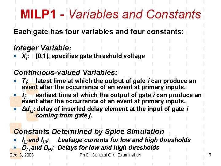
MILP 1 - Variables and Constants Each gate has four variables and four constants: Integer Variable: § Xi: [0, 1], specifies gate threshold voltage Continuous-valued Variables: § Ti: latest time at which the output of gate i can produce an event after the occurrence of an event at primary inputs. § ti: earliest time at which the output of gate i can produce an event after the occurrence of an event at primary inputs. § Δdi, j: delay of inserted delay element at the input of gate i coming from gate j. Constants Determined by Spice Simulation § ILi and IHi: Leakage currents for low and high thresholds § DLi and DHi: Delays for low and high thresholds Dec. 6, 2006 Ph. D. General Oral Examination 17

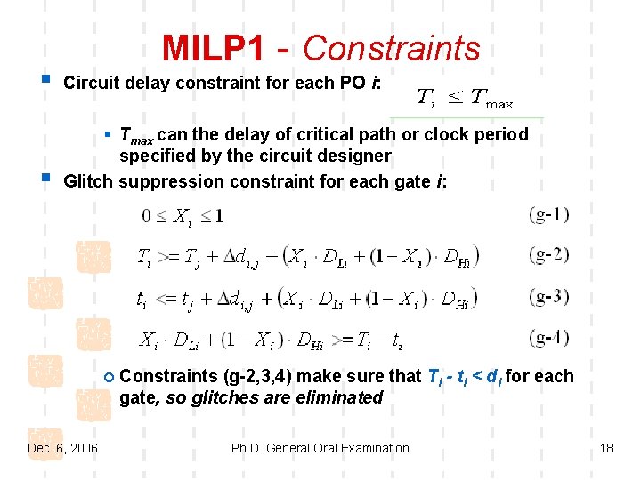
MILP 1 - Constraints § Circuit delay constraint for each PO i: § § Tmax can the delay of critical path or clock period specified by the circuit designer Glitch suppression constraint for each gate i: ¡ Constraints (g-2, 3, 4) make sure that Ti - ti < di for each gate, so glitches are eliminated Dec. 6, 2006 Ph. D. General Oral Examination 18

MILP 1 - gate constraints explained (t 0, T 0) (t 2, T 2) (1) (2) (3) (4) (5) Dec. 6, 2006 § Constraints 1 & 2 let T 2 be the largest arrival time at gate 2 output § Constraints 3 & 4 let t 2 be the earliest arrival time at gate 2 output § Constraint 5 makes sure that T 2 - t 2 < d 2 § D 2 can be a larger delay (high Vth) or a smaller delay (low Vth) Ph. D. General Oral Examination 19

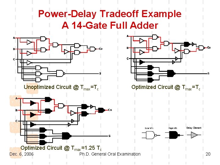
Power-Delay Tradeoff Example A 14 -Gate Full Adder Unoptimized Circuit @ Tmax=Tc Optimized Circuit @ Tmax=1. 25 Tc Dec. 6, 2006 Optimized Circuit @ Tmax=Tc Ph. D. General Oral Examination 20

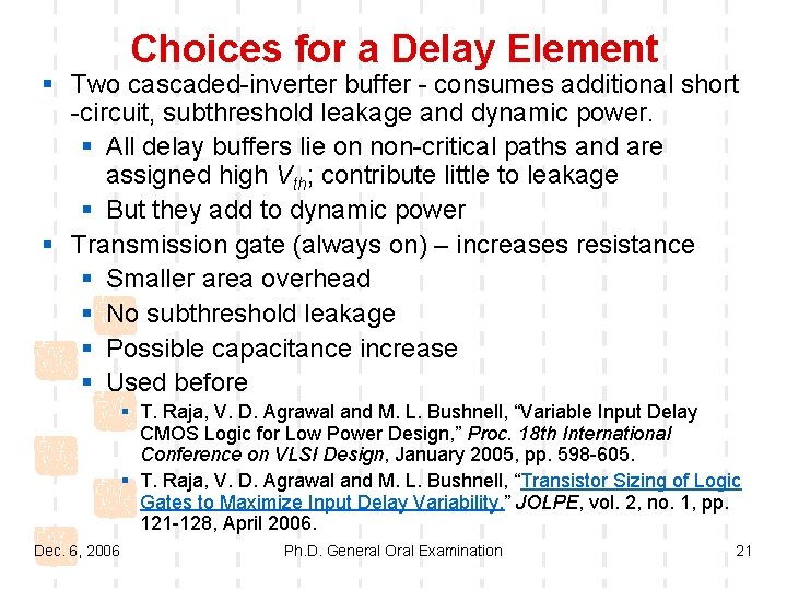
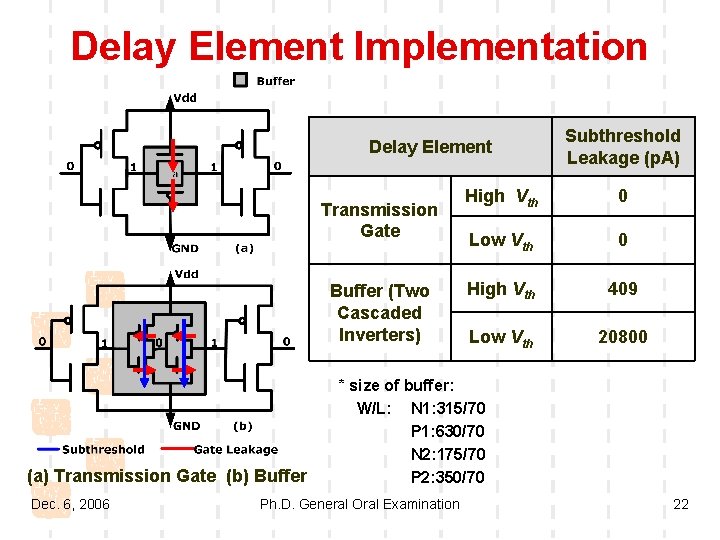
Choices for a Delay Element § Two cascaded-inverter buffer - consumes additional short -circuit, subthreshold leakage and dynamic power. § All delay buffers lie on non-critical paths and are assigned high Vth; contribute little to leakage § But they add to dynamic power § Transmission gate (always on) – increases resistance § Smaller area overhead § No subthreshold leakage § Possible capacitance increase § Used before § T. Raja, V. D. Agrawal and M. L. Bushnell, “Variable Input Delay CMOS Logic for Low Power Design, ” Proc. 18 th International Conference on VLSI Design, January 2005, pp. 598 -605. § T. Raja, V. D. Agrawal and M. L. Bushnell, “Transistor Sizing of Logic Gates to Maximize Input Delay Variability, ” JOLPE, vol. 2, no. 1, pp. 121 -128, April 2006. Dec. 6, 2006 Ph. D. General Oral Examination 21

Delay Element Implementation Delay Element Transmission Gate Buffer (Two Cascaded Inverters) (a) Transmission Gate (b) Buffer Dec. 6, 2006 Subthreshold Leakage (p. A) High Vth 0 Low Vth 0 High Vth 409 Low Vth 20800 * size of buffer: W/L: N 1: 315/70 P 1: 630/70 N 2: 175/70 P 2: 350/70 Ph. D. General Oral Examination 22

Outline § § Motivation Background Problem Statement Proposed Techniques Ø MILP 1 for Leakage and Glitch Minimization Ø MILP 2 for Statistical Leakage Optimization under Process Variation Ø Results § Conclusion § Future Work and Timeline Dec. 6, 2006 Ph. D. General Oral Examination 23

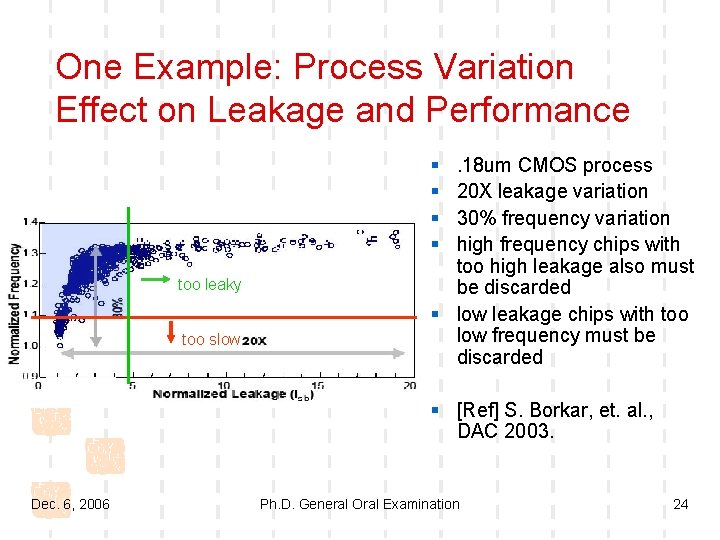
One Example: Process Variation Effect on Leakage and Performance § § too leaky too slow . 18 um CMOS process 20 X leakage variation 30% frequency variation high frequency chips with too high leakage also must be discarded § low leakage chips with too low frequency must be discarded § [Ref] S. Borkar, et. al. , DAC 2003. Dec. 6, 2006 Ph. D. General Oral Examination 24

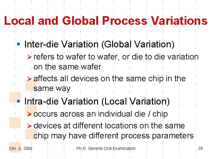
Local and Global Process Variations § Inter-die Variation (Global Variation) Ø refers to wafer, or die to die variation on the same wafer Ø affects all devices on the same chip in the same way § Intra-die Variation (Local Variation) Ø occurs across an individual die / chip Ø devices at different locations on the same chip may have different process parameters Dec. 6, 2006 Ph. D. General Oral Examination 25

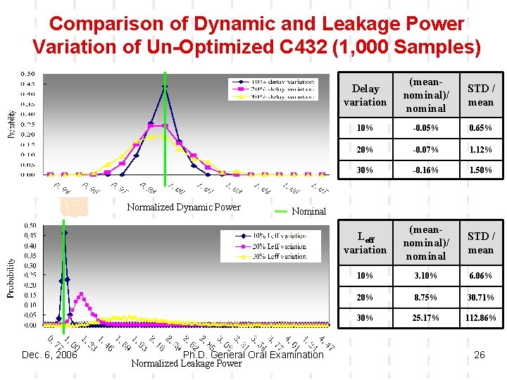
Comparison of Dynamic and Leakage Power Variation of Un-Optimized C 432 (1, 000 Samples) Normalized Dynamic Power Dec. 6, 2006 Delay variation (meannominal)/ nominal STD / mean 10% -0. 05% 0. 65% 20% -0. 07% 1. 12% 30% -0. 16% 1. 50% Leff variation (meannominal)/ nominal STD / mean 10% 3. 10% 6. 06% 20% 8. 75% 30. 71% 30% 25. 17% 112. 86% Nominal Ph. D. General Oral Examination Normalized Leakage Power 26

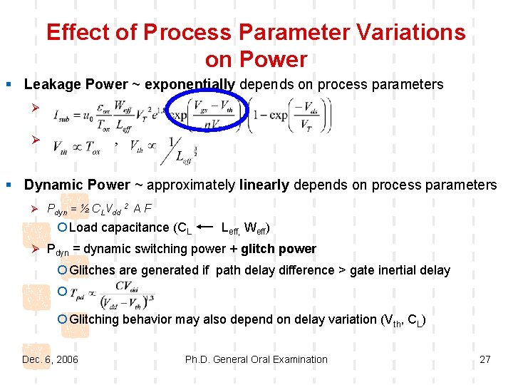
Effect of Process Parameter Variations on Power § Leakage Power ~ exponentially depends on process parameters Ø , Ø § Dynamic Power ~ approximately linearly depends on process parameters Ø Pdyn = ½ CLVdd 2 AF ¡ Load capacitance (CL Leff, Weff) Ø Pdyn = dynamic switching power + glitch power ¡ Glitches are generated if path delay difference > gate inertial delay ¡ ¡ Glitching behavior may also depend on delay variation (Vth, CL) Dec. 6, 2006 Ph. D. General Oral Examination 27

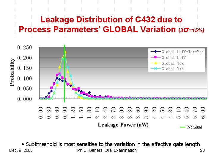
Leakage Distribution of C 432 due to Process Parameters' GLOBAL Variation (3σ=15%) Nominal • Subthreshold is most sensitive to the variation in the effective gate length. Dec. 6, 2006 Ph. D. General Oral Examination 28

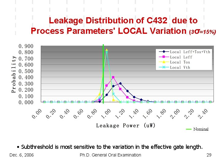
Leakage Distribution of C 432 due to Process Parameters' LOCAL Variation (3σ=15%) Nominal • Subthreshold is most sensitive to the variation in the effective gate length. Dec. 6, 2006 Ph. D. General Oral Examination 29

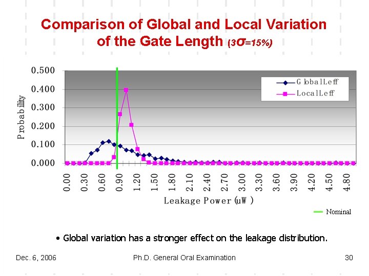
Comparison of Global and Local Variation of the Gate Length (3σ=15%) Nominal • Global variation has a stronger effect on the leakage distribution. Dec. 6, 2006 Ph. D. General Oral Examination 30

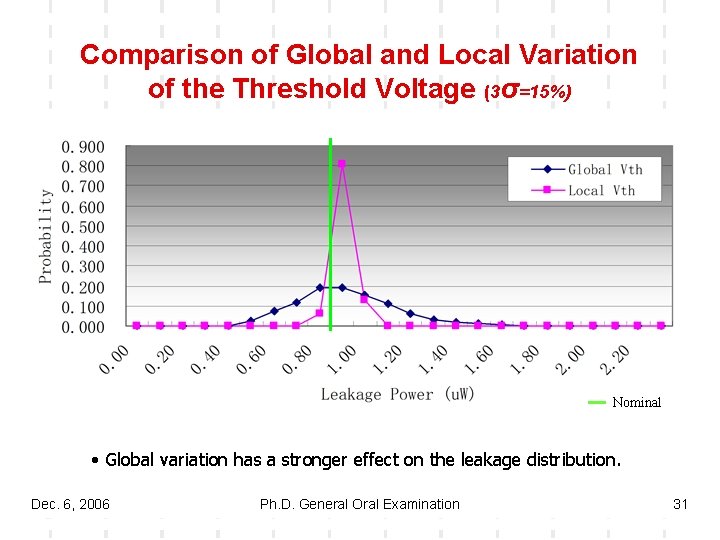
Comparison of Global and Local Variation of the Threshold Voltage (3σ=15%) Nominal • Global variation has a stronger effect on the leakage distribution. Dec. 6, 2006 Ph. D. General Oral Examination 31

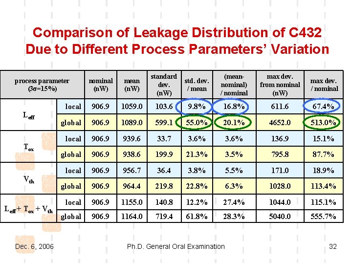
Comparison of Leakage Distribution of C 432 Due to Different Process Parameters’ Variation nominal (n. W) mean (n. W) standard dev. (n. W) std. dev. / mean (meannominal) / nominal max dev. from nominal (n. W) max dev. / nominal local 906. 9 1059. 0 103. 6 9. 8% 16. 8% 611. 6 67. 4% global 906. 9 1089. 0 599. 1 55. 0% 20. 1% 4652. 0 513. 0% local 906. 9 939. 6 33. 7 3. 6% 136. 9 15. 1% global 906. 9 938. 6 199. 9 21. 3% 3. 5% 795. 8 87. 7% local 906. 9 956. 7 36. 4 3. 8% 5. 5% 171. 0 18. 9% global 906. 9 964. 4 219. 8 22. 8% 6. 3% 1028. 0 113. 4% local 906. 9 1155. 0 140. 8 12. 2% 27. 4% 1044. 0 115. 1% global 906. 9 1164. 0 719. 4 61. 8% 28. 3% 5040. 0 555. 7% process parameter (3σ=15%) Leff Tox Vth Leff + Tox + Vth Dec. 6, 2006 Ph. D. General Oral Examination 32
![Statistical Leakage Modeling Deterministic Statistical lognormal distribution ref Statistical of Total Leakage Statistical Leakage Modeling Deterministic Statistical – lognormal distribution [ref] Statistical of Total Leakage –](https://slidetodoc.com/presentation_image_h2/9dd1c3e5798cd2e196c8ee60cf14a589/image-33.jpg)
Statistical Leakage Modeling Deterministic Statistical – lognormal distribution [ref] Statistical of Total Leakage – approximately lognormal distribution [ref] R. Rao, et. al. DAC 2004. Dec. 6, 2006 Ph. D. General Oral Examination 33
![Statistical Delay Modeling Deterministic Statistical normal distribution ref Let Xi is a process Statistical Delay Modeling Deterministic Statistical – normal distribution [ref] Let Xi is a process](https://slidetodoc.com/presentation_image_h2/9dd1c3e5798cd2e196c8ee60cf14a589/image-34.jpg)
Statistical Delay Modeling Deterministic Statistical – normal distribution [ref] Let Xi is a process parameter, Xi 0 is the nominal value of Xi Mean Standard Deviation Let {X 1, X 2, X 3} = {Leff, Tox, Ndop} Dec. 6, 2006 [ref] A. Davoodi and A. Srivastava, ISLPED, 2005. Ph. D. General Oral Examination 34

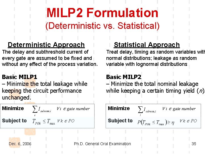
MILP 2 Formulation (Deterministic vs. Statistical) Deterministic Approach Statistical Approach The delay and subthreshold current of every gate are assumed to be fixed and without any effect of the process variation. Treat delay, timing as random variables with normal distributions; leakage as random variable with lognormal distributions Basic MILP 1 – Minimize the total leakage while keeping the circuit performance unchanged. Basic MILP 2 – Minimize the total nominal leakage while keeping a certain timing yield (n). Minimize " i Î gate number Minimize Subject to " k Î PO Subject to Dec. 6, 2006 Ph. D. General Oral Examination " i Î gate number " k Î PO 35

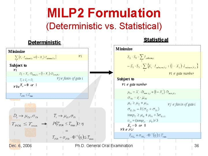
MILP 2 Formulation (Deterministic vs. Statistical) Statistical Deterministic Minimize "i Subject to "i " i Î gate number " jÎ fanin of gate i Subject to " i Î gate number " kÎPO " j Î fan in of gate i = Dec. 6, 2006 " k Î PO Ph. D. General Oral Examination 36

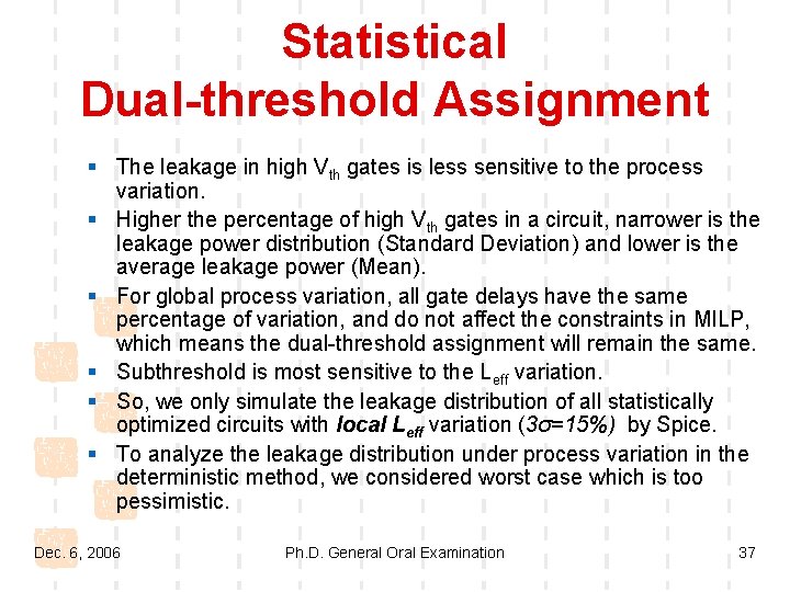
Statistical Dual-threshold Assignment § The leakage in high Vth gates is less sensitive to the process variation. § Higher the percentage of high Vth gates in a circuit, narrower is the leakage power distribution (Standard Deviation) and lower is the average leakage power (Mean). § For global process variation, all gate delays have the same percentage of variation, and do not affect the constraints in MILP, which means the dual-threshold assignment will remain the same. § Subthreshold is most sensitive to the Leff variation. § So, we only simulate the leakage distribution of all statistically optimized circuits with local Leff variation (3σ=15%) by Spice. § To analyze the leakage distribution under process variation in the deterministic method, we considered worst case which is too pessimistic. Dec. 6, 2006 Ph. D. General Oral Examination 37

Outline § § Motivation Problem Statement Background Proposed Techniques Ø MILP 1 for Leakage and Glitch Minimization Ø MILP 2 for Statistical Leakage Optimization under Process Variation Ø Results § Conclusion § Future Work and Timeline Dec. 6, 2006 Ph. D. General Oral Examination 38

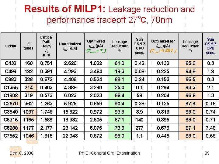
Results of MILP 1: Leakage reduction and performance tradeoff 27℃, 70 nm Circuit # gates Critical Path Delay Tc (ns) C 432 160 0. 751 2. 620 1. 022 61. 0 0. 42 0. 132 95. 0 0. 3 C 499 182 0. 391 4. 293 3. 464 19. 3 0. 08 0. 225 94. 8 1. 8 C 880 328 0. 672 4. 406 0. 524 88. 1 0. 24 0. 153 96. 5 0. 3 C 1355 214 0. 403 4. 388 3. 290 25. 0 0. 1 0. 294 93. 3 2. 1 C 1908 319 0. 573 6. 023 2. 023 66. 4 59 0. 204 96. 6 1. 3 C 2670 362 1. 263 5. 925 0. 659 90. 4 0. 38 0. 125 97. 9 0. 16 C 3540 1097 1. 748 15. 622 0. 972 93. 8 3. 9 0. 319 98. 0 0. 74 C 5315 1165 1. 589 19. 332 2. 505 87. 1 140 0. 395 98. 0 0. 71 C 6288 1177 23. 142 6. 075 73. 8 277 0. 678 97. 1 7. 48 C 7552 1046 1. 915 22. 043 0. 872 96. 0 1. 1 0. 445 98. 0 0. 58 Dec. 6, 2006 Unoptimized Ileak (μA) Optimized Ileak (μA) (Tmax= Tc ) Leakage Reduction % Sun OS 5. 7 CPU secs. Optimized for Ileak (μA) (Tmax=1. 25 Tc ) Leakage Reduction % Sun OS 5. 7 CPU secs. Ph. D. General Oral Examination 39

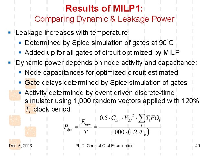
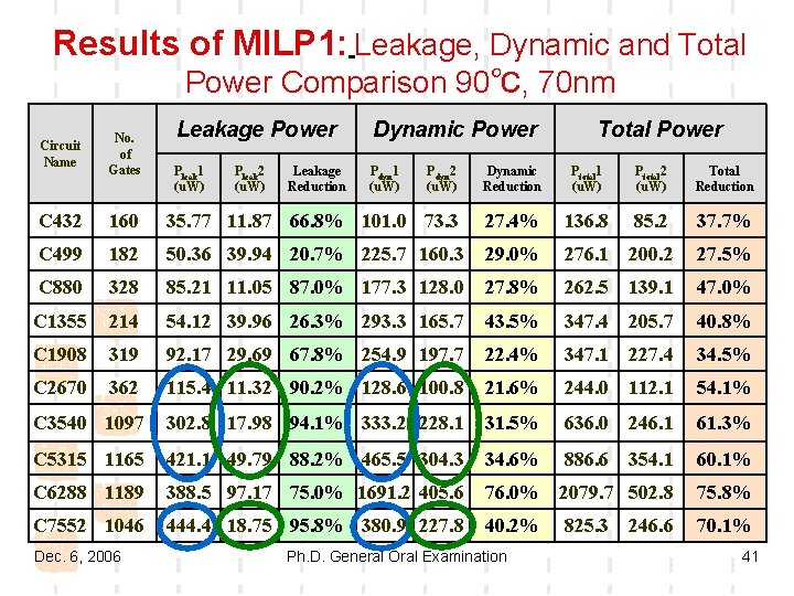
Results of MILP 1: Comparing Dynamic & Leakage Power § Leakage increases with temperature: § Determined by Spice simulation of gates at 90ºC § Added up for all gates of circuit optimized by MILP § Dynamic power depends on node activity and capacitance: § Node capacitances for optimized circuit estimated § Gate delays determined by Spice simulation of gates § Activity determined by event driven discrete-time simulator using 1, 000 random vectors applied with 120% Tc clock period Dec. 6, 2006 Ph. D. General Oral Examination 40

Results of MILP 1: Leakage, Dynamic and Total Power Comparison 90℃, 70 nm Circuit Name No. of Gates C 432 Leakage Power Dynamic Power Pleak 1 (u. W) Pdyn 2 (u. W) Dynamic Reduction Ptotal 1 (u. W) Ptotal 2 (u. W) Total Reduction 160 35. 77 11. 87 66. 8% 101. 0 73. 3 27. 4% 136. 8 85. 2 37. 7% C 499 182 50. 36 39. 94 20. 7% 225. 7 160. 3 29. 0% 276. 1 200. 2 27. 5% C 880 328 85. 21 11. 05 87. 0% 177. 3 128. 0 27. 8% 262. 5 139. 1 47. 0% C 1355 214 54. 12 39. 96 26. 3% 293. 3 165. 7 43. 5% 347. 4 205. 7 40. 8% C 1908 319 92. 17 29. 69 67. 8% 254. 9 197. 7 22. 4% 347. 1 227. 4 34. 5% C 2670 362 115. 4 11. 32 90. 2% 128. 6 100. 8 21. 6% 244. 0 112. 1 54. 1% C 3540 1097 302. 8 17. 98 94. 1% 333. 2 228. 1 31. 5% 636. 0 246. 1 61. 3% C 5315 1165 421. 1 49. 79 88. 2% 465. 5 304. 3 34. 6% 886. 6 354. 1 60. 1% C 6288 1189 388. 5 97. 17 75. 0% 1691. 2 405. 6 76. 0% 2079. 7 502. 8 75. 8% C 7552 1046 444. 4 18. 75 95. 8% 380. 9 227. 8 40. 2% 70. 1% Dec. 6, 2006 Pleak 2 (u. W) Leakage Reduction Total Power Ph. D. General Oral Examination 825. 3 246. 6 41

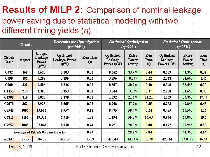
Results of MILP 2: Comparison of nominal leakage power saving due to statistical modeling with two different timing yields (η). Deterministic Optimization (η=100%) Circuit Statistical Optimization (η=99%) Statistical Optimization (η=95%) Circuit Name # gates Un-opt. Leakage Power (μW) C 432 160 2. 620 1. 003 0. 00 0. 662 33. 9% 0. 44 0. 589 41. 3% 0. 32 C 499 182 4. 293 3. 396 0. 02 3. 396 0. 0% 0. 22 2. 323 31. 6% 1. 47 C 880 328 4. 406 0. 526 0. 02 0. 367 30. 2% 0. 18 0. 340 35. 4% 0. 18 C 1355 214 4. 388 3. 153 0. 00 3. 044 3. 5% 0. 17 2. 158 31. 6% 0. 48 C 1908 319 6. 023 1. 179 0. 03 1. 392 21. 7% 11. 21 1. 169 34. 3% 17. 45 C 2670 362 5. 925 0. 565 0. 03 0. 298 47. 2% 0. 35 0. 283 49. 8% 0. 43 C 3540 1097 15. 622 0. 957 0. 13 0. 475 50. 4% 0. 24 0. 435 54. 5% 1. 17 C 5315 1165 19. 332 2. 716 1. 88 1. 194 56. 0% 67. 63 0. 956 64. 8% 19. 7 C 7552 1045 22. 043 0. 938 0. 44 0. 751 20. 0% 0. 88 0. 677 27. 9% 0. 58 29. 2% 9. 04 41. 3% 4. 64 14. 07% 36. 79 14. 07% 36. 44 Optimized Leakage Power (μW) Run Time (s) Optimized Leakage Power (μW) Extra Power Saving Run Time (s) Average of ISCAS’ 85 benchmarks ARM 7 15. 5 k Dec. 6, 2006 686. 56 495. 12 0. 24 15. 69 425. 44 Ph. D. General Oral Examination 425. 44 42

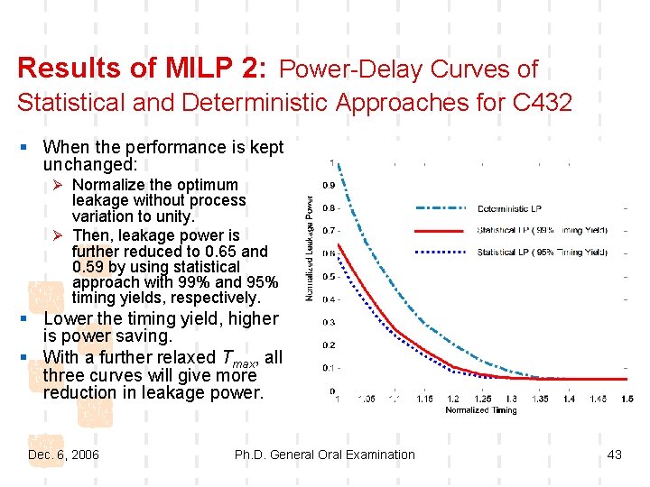
Results of MILP 2: Power-Delay Curves of Statistical and Deterministic Approaches for C 432 § When the performance is kept unchanged: Ø Normalize the optimum leakage without process variation to unity. Ø Then, leakage power is further reduced to 0. 65 and 0. 59 by using statistical approach with 99% and 95% timing yields, respectively. § Lower the timing yield, higher is power saving. § With a further relaxed Tmax, all three curves will give more reduction in leakage power. Dec. 6, 2006 Ph. D. General Oral Examination 43

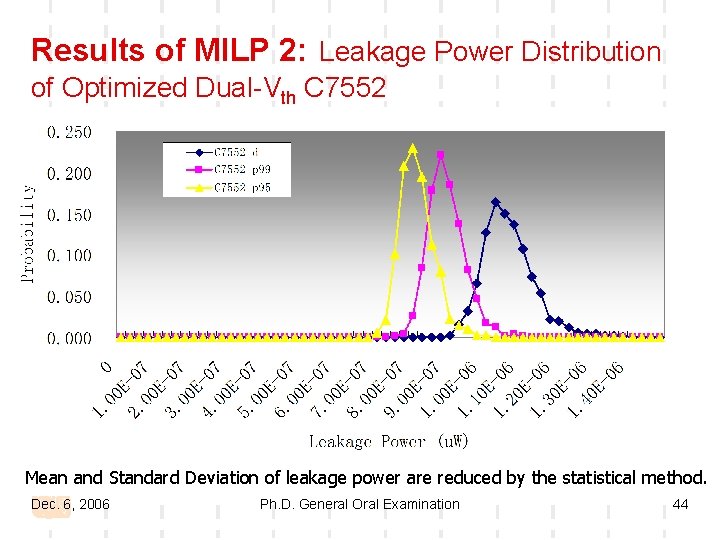
Results of MILP 2: Leakage Power Distribution of Optimized Dual-Vth C 7552 Mean and Standard Deviation of leakage power are reduced by the statistical method. Dec. 6, 2006 Ph. D. General Oral Examination 44

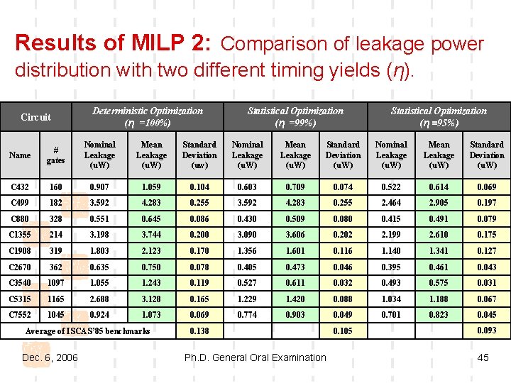
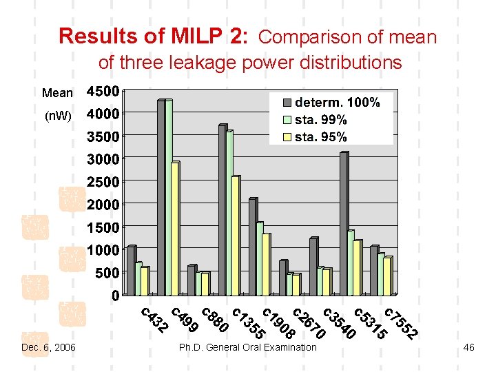
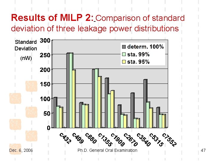
Results of MILP 2: Comparison of leakage power distribution with two different timing yields (η). Circuit Deterministic Optimization (η =100%) Statistical Optimization (η =99%) Statistical Optimization (η =95%) Name # gates Nominal Leakage (u. W) Mean Leakage (u. W) Standard Deviation (uw) Nominal Leakage (u. W) Mean Leakage (u. W) Standard Deviation (u. W) C 432 160 0. 907 1. 059 0. 104 0. 603 0. 709 0. 074 0. 522 0. 614 0. 069 C 499 182 3. 592 4. 283 0. 255 2. 464 2. 905 0. 197 C 880 328 0. 551 0. 645 0. 086 0. 430 0. 509 0. 080 0. 415 0. 491 0. 079 C 1355 214 3. 198 3. 744 0. 200 3. 090 3. 606 0. 202 2. 199 2. 610 0. 175 C 1908 319 1. 803 2. 123 0. 170 1. 356 1. 601 0. 116 1. 140 1. 341 0. 127 C 2670 362 0. 635 0. 750 0. 078 0. 405 0. 473 0. 046 0. 395 0. 461 0. 043 C 3540 1097 1. 055 1. 243 0. 119 0. 527 0. 611 0. 032 0. 493 0. 575 0. 031 C 5315 1165 2. 688 3. 128 0. 165 1. 229 1. 420 0. 088 1. 034 1. 188 0. 067 C 7552 1045 0. 924 1. 073 0. 069 0. 774 0. 903 0. 049 0. 701 0. 823 0. 045 Average of ISCAS’ 85 benchmarks Dec. 6, 2006 0. 138 Ph. D. General Oral Examination 0. 105 0. 093 45

Results of MILP 2: Comparison of mean of three leakage power distributions Mean (n. W) Dec. 6, 2006 Ph. D. General Oral Examination 46

Results of MILP 2: Comparison of standard deviation of three leakage power distributions Standard Deviation (n. W) Dec. 6, 2006 Ph. D. General Oral Examination 47

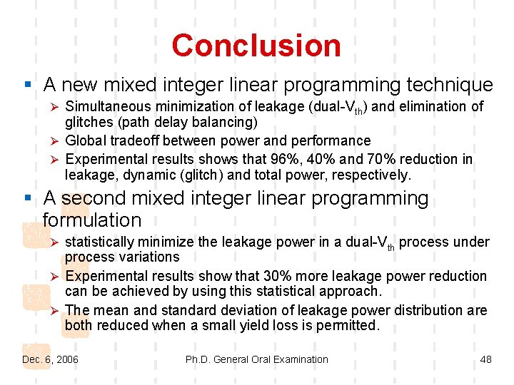
Conclusion § A new mixed integer linear programming technique Ø Simultaneous minimization of leakage (dual-Vth) and elimination of glitches (path delay balancing) Ø Global tradeoff between power and performance Ø Experimental results shows that 96%, 40% and 70% reduction in leakage, dynamic (glitch) and total power, respectively. § A second mixed integer linear programming formulation Ø statistically minimize the leakage power in a dual-Vth process under process variations Ø Experimental results show that 30% more leakage power reduction can be achieved by using this statistical approach. Ø The mean and standard deviation of leakage power distribution are both reduced when a small yield loss is permitted. Dec. 6, 2006 Ph. D. General Oral Examination 48

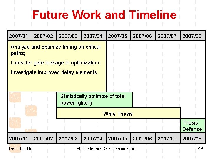
Future Work and Timeline 2007/01 2007/02 2007/03 2007/04 2007/05 2007/06 2007/07 2007/08 Analyze and optimize timing on critical paths; Consider gate leakage in optimization; Investigate improved delay elements. Statistically optimize of total power (glitch) Write Thesis Defense 2007/01 Dec. 6, 2006 2007/02 2007/03 2007/04 2007/05 2007/06 Ph. D. General Oral Examination 2007/07 2007/08 49

Thank You All ! Questions? Dec. 6, 2006 Ph. D. General Oral Examination 50