Power Amplifier Design using ADS PA Workshop Wilfredo


- Slides: 49

Power Amplifier Design using ADS PA Workshop Wilfredo Rivas-Torres Technical Support Application Engineer October 12, 2004 1

Outline • • • Introduction DC and Loadline analysis Bias and Stability Load. Pull Matching using Smith Chart Utility Source. Pull PA Characterization – Did we meet the specification? Optimize/Fine Tune the design Test Design with real world modulated signals Layout ADS Power Amp Design 2

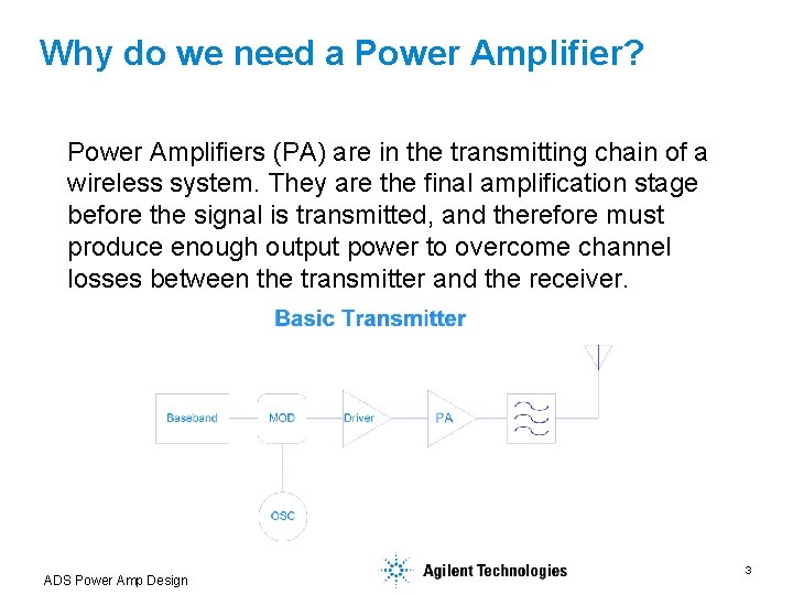
Why do we need a Power Amplifier? Power Amplifiers (PA) are in the transmitting chain of a wireless system. They are the final amplification stage before the signal is transmitted, and therefore must produce enough output power to overcome channel losses between the transmitter and the receiver. ADS Power Amp Design 3

PA requirements • The PA is typically the primary consumer of power in a transmitter. A major design requirement is how efficiently the PA can convert DC power to RF output power. • The design engineer has to often concern himself with the Efficiency of the Power Amplifier. Notice that efficiency translates into either lower operation cost (e. g. cellular basestation) or longer battery life (e. g. wireless handheld). • PA linearity is another important requirement, the input/ output relationship must be linear to preserve the signal integrity. • The design of PAs often involves the tradeoff of efficiency and linearity. ADS Power Amp Design 4

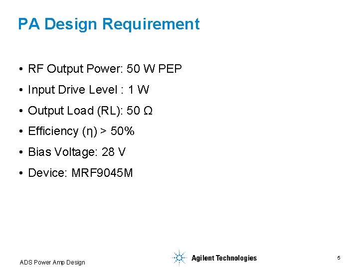
PA Design Requirement • RF Output Power: 50 W PEP • Input Drive Level : 1 W • Output Load (RL): 50 Ω • Efficiency (η) > 50% • Bias Voltage: 28 V • Device: MRF 9045 M ADS Power Amp Design 5

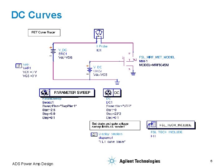
DC Curves ADS Power Amp Design 6

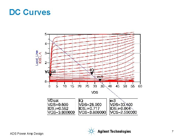
DC Curves ADS Power Amp Design 7

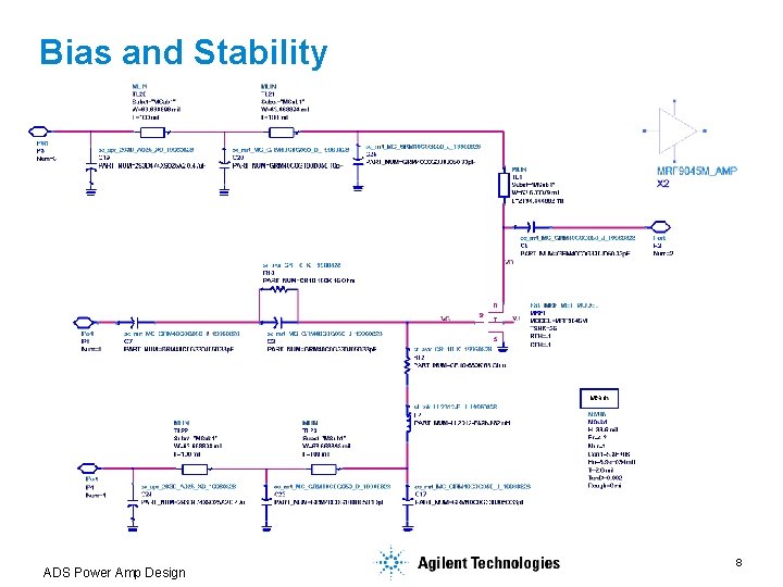
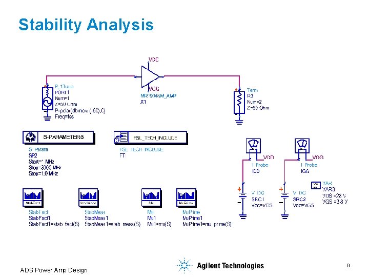
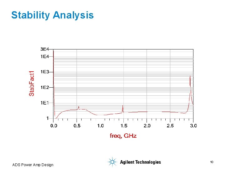
Bias and Stability ADS Power Amp Design 8

Stability Analysis ADS Power Amp Design 9

Stability Analysis ADS Power Amp Design 10

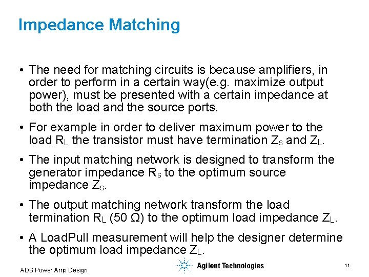
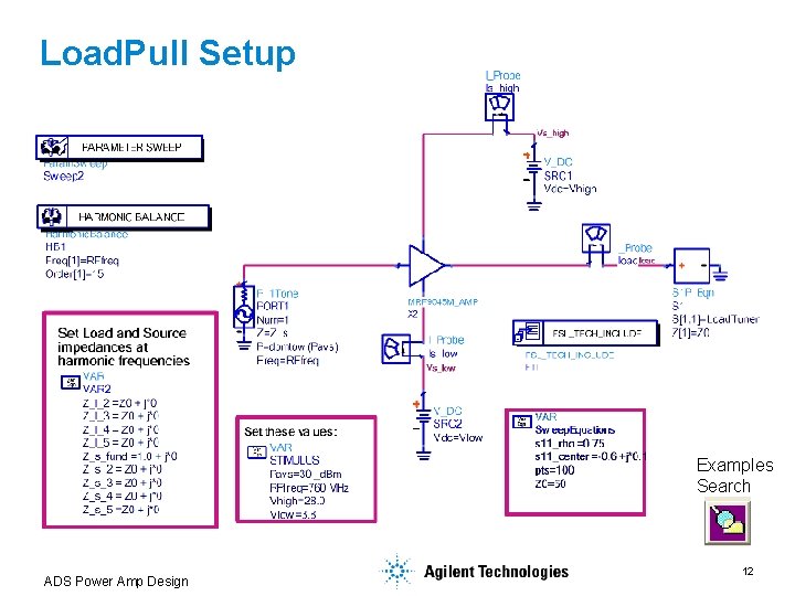
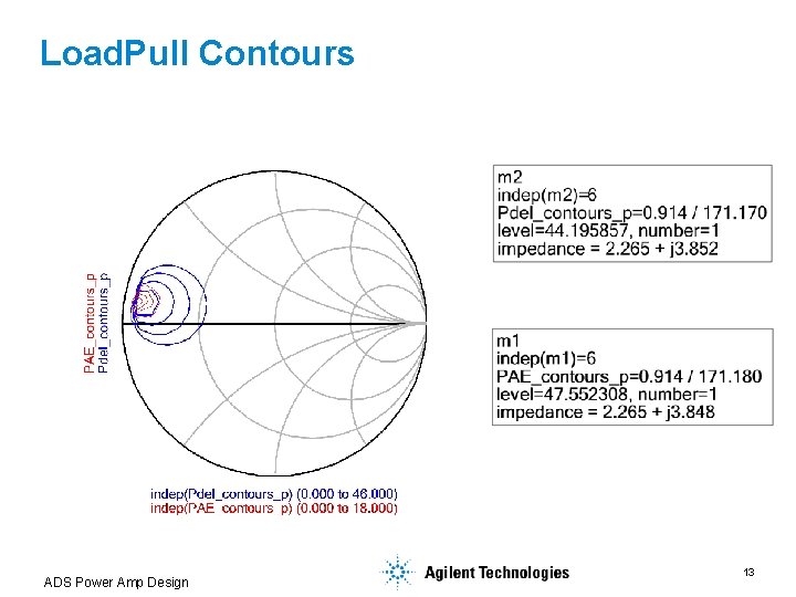
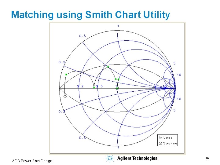
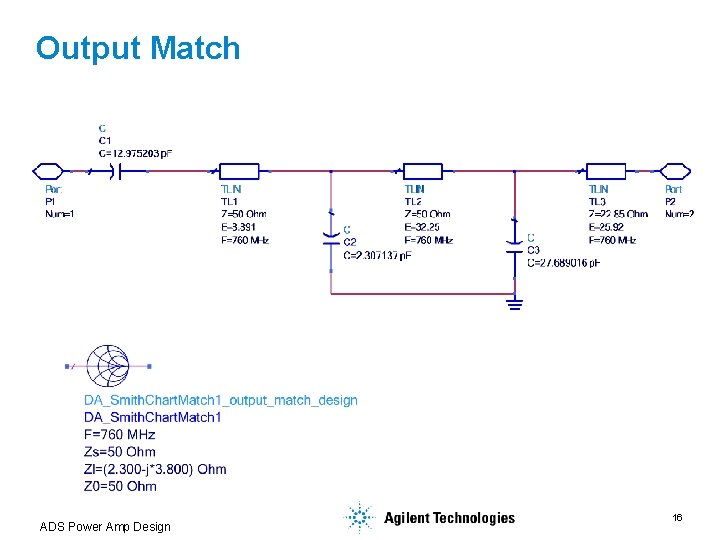
Impedance Matching • The need for matching circuits is because amplifiers, in order to perform in a certain way(e. g. maximize output power), must be presented with a certain impedance at both the load and the source ports. • For example in order to deliver maximum power to the load RL the transistor must have termination Zs and ZL. • The input matching network is designed to transform the generator impedance Rs to the optimum source impedance Zs. • The output matching network transform the load termination RL (50 Ω) to the optimum load impedance ZL. • A Load. Pull measurement will help the designer determine the optimum load impedance ZL. ADS Power Amp Design 11

Load. Pull Setup Examples Search ADS Power Amp Design 12

Load. Pull Contours ADS Power Amp Design 13

Matching using Smith Chart Utility ADS Power Amp Design 14

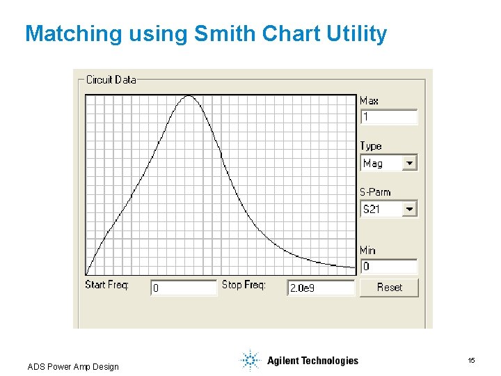
Matching using Smith Chart Utility ADS Power Amp Design 15

Output Match ADS Power Amp Design 16

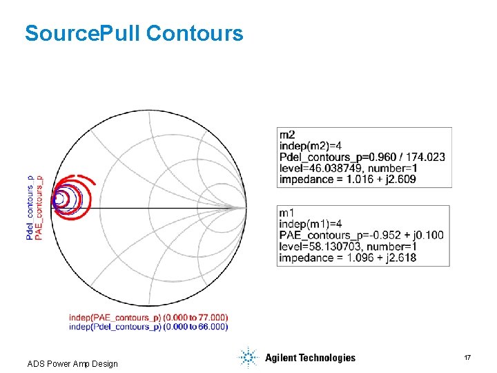
Source. Pull Contours ADS Power Amp Design 17

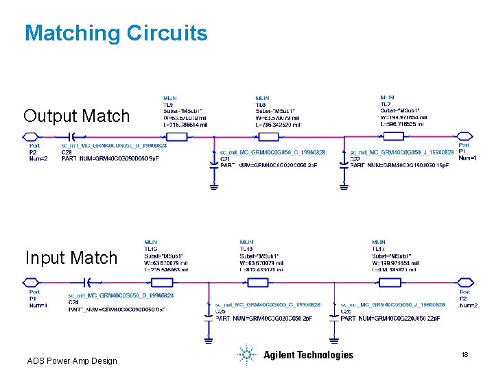
Matching Circuits Output Match Input Match ADS Power Amp Design 18

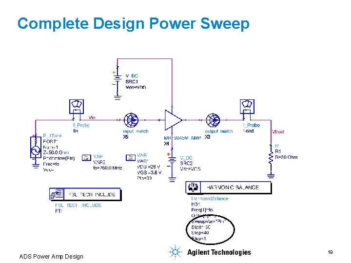
Complete Design Power Sweep ADS Power Amp Design 19

Power Compression Curve ADS Power Amp Design 20

Gain Compression Curve ADS Power Amp Design 21

Power Added Efficiency ADS Power Amp Design 22

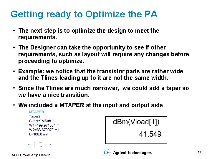
Getting ready to Optimize the PA • The next step is to optimize the design to meet the requirements. • The Designer can take the opportunity to see if other requirements, such as layout will require any changes before proceeding to optimize. • Example: we notice that the transistor pads are rather wide and the Tlines leading up to it are not the same width. • Since the Tlines are much narrower, we could add a taper so we have a nice transition. • We included a MTAPER at the input and output side ADS Power Amp Design 23

Optimization Setup ADS Power Amp Design 24

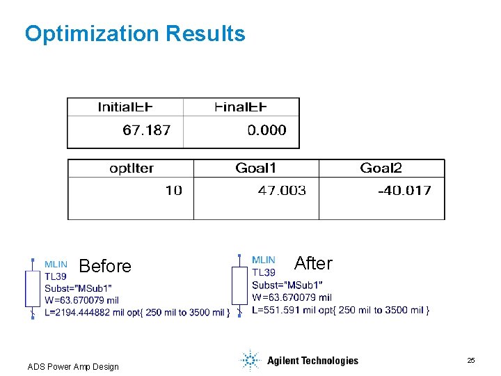
Optimization Results Before ADS Power Amp Design After 25

Optimization Values ADS Power Amp Design 26

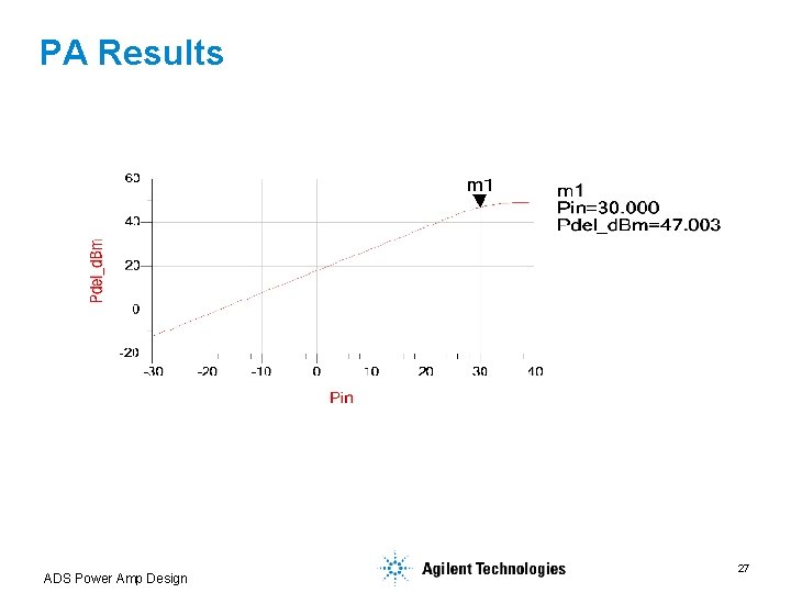
PA Results ADS Power Amp Design 27

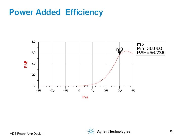
Power Added Efficiency ADS Power Amp Design 28

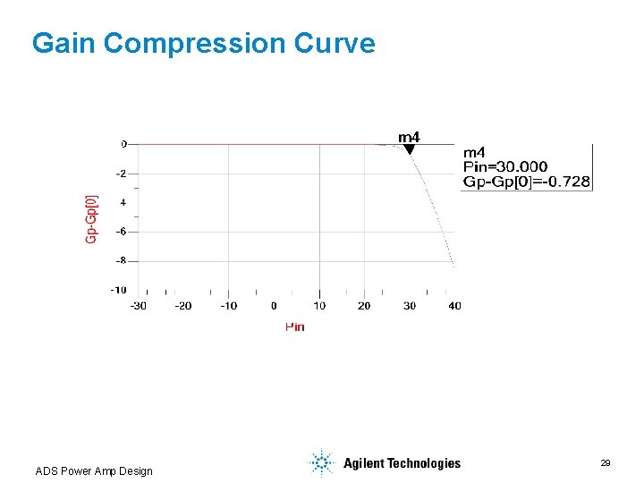
Gain Compression Curve ADS Power Amp Design 29

Complex Modulated Signal ADS Power Amp Design 30

16 QAM Modulated Source ADS Power Amp Design 31

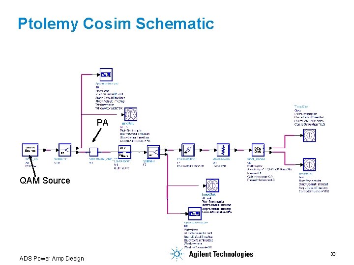
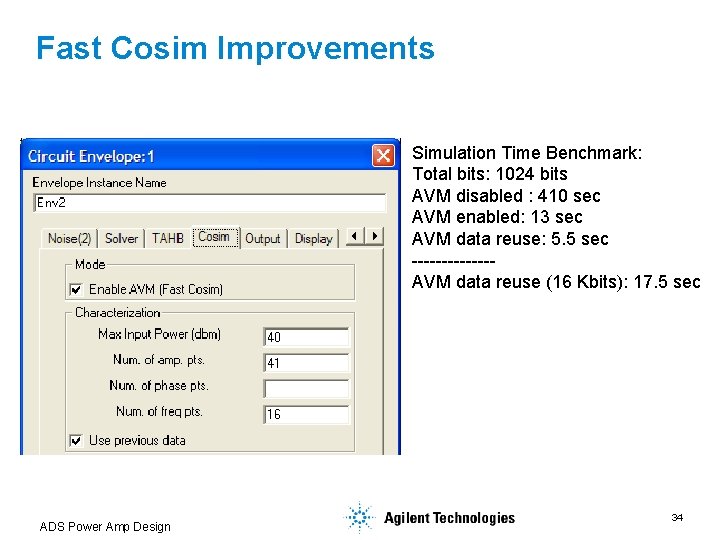
DSP and Analog Circuits Setup • Create a subcircuit with your analog design. • You need to add either Circuit Envelope or Transient controller to the analog circuit. • We use Circuit Envelope specifically with our PA since we have a Modulated Carrier. • Circuit Envelope will also allow the use of Fast Cosim (Automatic Verification Modeling – AVM). This will dramatically increase the simulation speed. • In the DSP schematic we will create the Modulated Carrier, feed it to the PA and collect the signal samples and spectrum. • The DSP schematic contains a Envelope Output Selector component used for interfacing between circuit subnetwork output and the signal processing components. ADS Power Amp Design 32

Ptolemy Cosim Schematic PA QAM Source ADS Power Amp Design 33

Fast Cosim Improvements Simulation Time Benchmark: Total bits: 1024 bits AVM disabled : 410 sec AVM enabled: 13 sec AVM data reuse: 5. 5 sec -------AVM data reuse (16 Kbits): 17. 5 sec ADS Power Amp Design 34

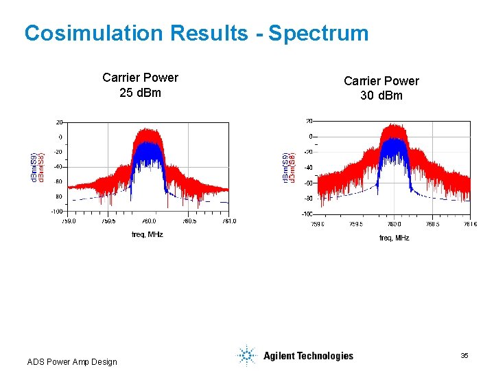
Cosimulation Results - Spectrum Carrier Power 25 d. Bm ADS Power Amp Design Carrier Power 30 d. Bm 35

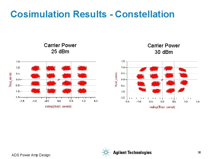
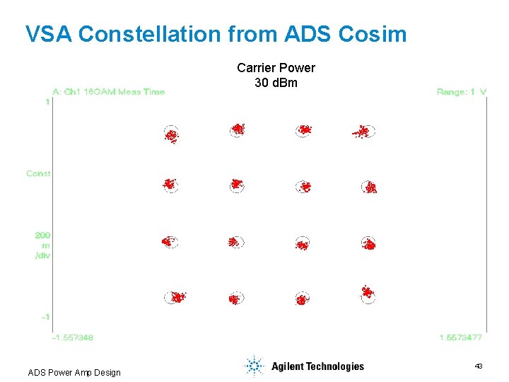
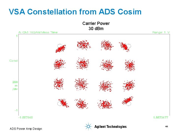
Cosimulation Results - Constellation Carrier Power 25 d. Bm ADS Power Amp Design Carrier Power 30 d. Bm 36

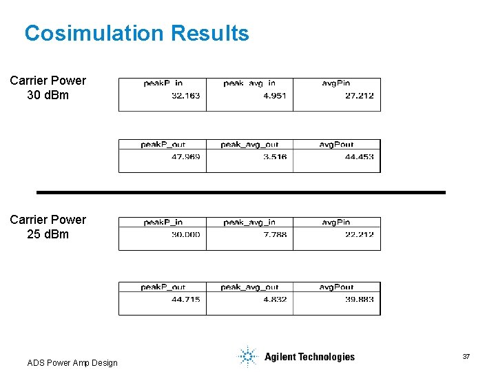
Cosimulation Results Carrier Power 30 d. Bm Carrier Power 25 d. Bm ADS Power Amp Design 37

Cosimulation Results – CCDF Carrier Power 25 d. Bm ADS Power Amp Design Carrier Power 30 d. Bm 38

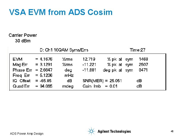
EVM vs. Power Measurement ADS Power Amp Design 39

EVM vs. Power Results ADS Power Amp Design 40

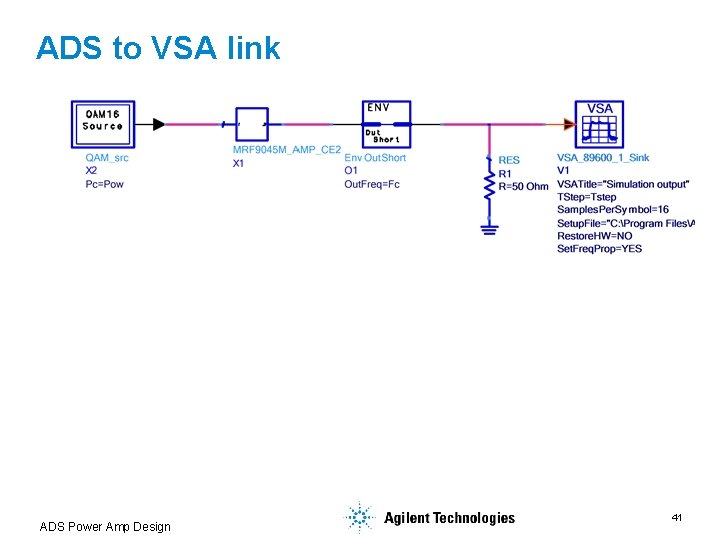
ADS to VSA link ADS Power Amp Design 41

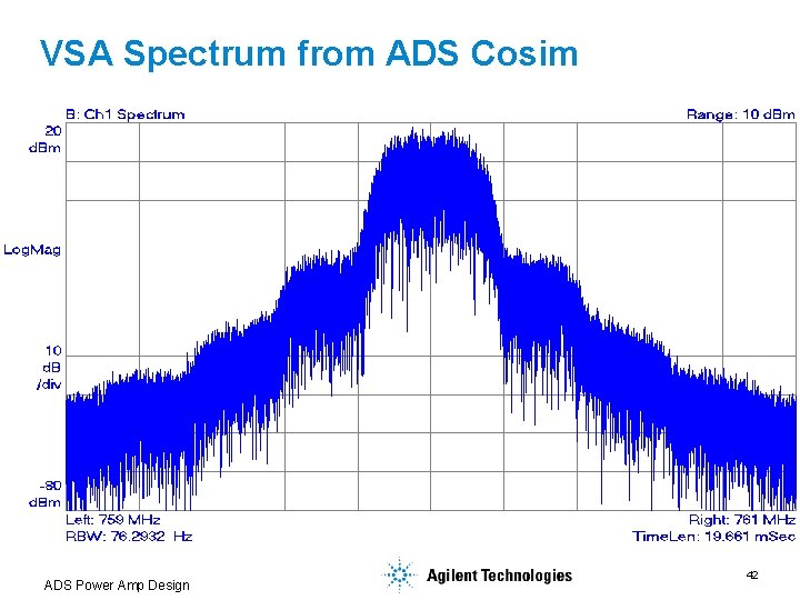
VSA Spectrum from ADS Cosim ADS Power Amp Design 42

VSA Constellation from ADS Cosim Carrier Power 30 d. Bm ADS Power Amp Design 43

VSA Constellation from ADS Cosim Carrier Power 30 d. Bm ADS Power Amp Design 44

VSA EVM from ADS Cosim Carrier Power 30 d. Bm ADS Power Amp Design 45

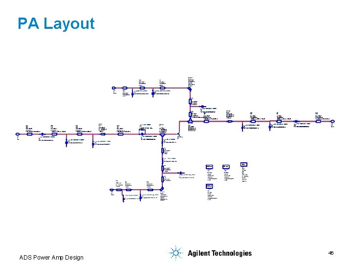
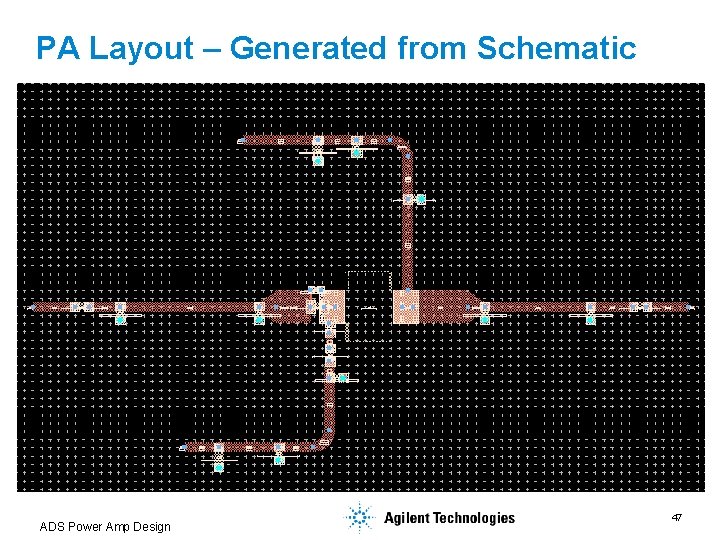
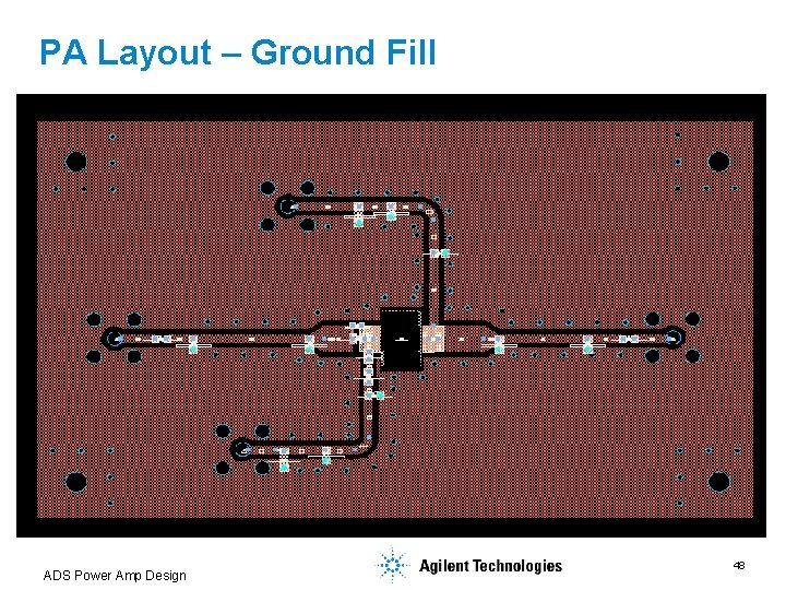
PA Layout ADS Power Amp Design 46

PA Layout – Generated from Schematic ADS Power Amp Design 47

PA Layout – Ground Fill ADS Power Amp Design 48

Other Possibilities • Run an EM Cosimulation – include layout effects in the simulation. Optimize design if necessary. • Run Loadpull for IP 3 or ACPR. The optimum load would then be a compromise between all the requirements. • Use Connection Manager and real PA to validate design and compare vs. simulated results. • Create a behavioral data model that can be used to protect you IP yet give access to your design results. If there is any topic about PA Design and ADS you wish to discuss email me: wilfredo_rivas-torres@agilent. com ADS Power Amp Design 49