PostRouting BEOL Layout Optimization for Improved Time Dependent

Post-Routing BEOL Layout Optimization for Improved Time. Dependent Dielectric Breakdown (TDDB) Reliability Tuck-Boon Chan and Andrew B. Kahng VLSI CAD LABORATORY, UC San Diego VLSI CAD Laboratory, UC San Diego -1 -

Outline n TDDB Reliability n Our work: reducing TDDB Margin – Signal-aware TDDB Analysis – Post-routing Layout Optimization n Experimental Results and Conclusions -2 -
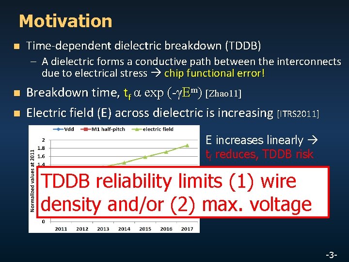
Motivation n Time-dependent dielectric breakdown (TDDB) – A dielectric forms a conductive path between the interconnects due to electrical stress chip functional error! n n Breakdown time, tf α exp (-γEm) [Zhao 11] Electric field (E) across dielectric is increasing [ITRS 2011] E increases linearly tf reduces, TDDB risk TDDB reliability limits (1) wire density and/or (2) max. voltage -3 -
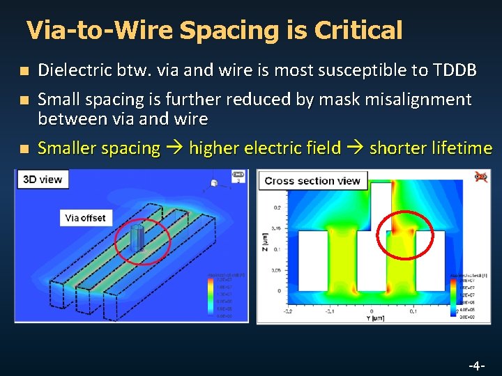
Via-to-Wire Spacing is Critical n n n Dielectric btw. via and wire is most susceptible to TDDB Small spacing is further reduced by mask misalignment between via and wire Smaller spacing higher electric field shorter lifetime -4 -

Our Work (1) n A chip-level TDDB reliability model – Enable signal-aware TDDB analysis -5 -
![TDDB Model n Dielectric breakdown time is modeled as a Weibull distribution [Bashir 10] TDDB Model n Dielectric breakdown time is modeled as a Weibull distribution [Bashir 10]](http://slidetodoc.com/presentation_image_h/96aa91da06062af396509690c80f7997/image-6.jpg)
TDDB Model n Dielectric breakdown time is modeled as a Weibull distribution [Bashir 10] Failure probability Fij(t) = 1 – ( exp(-t/nij )β ) Weibull shape factor Characteristic lifetime nij = A exp(-γ(V/Sij)m ) Supply voltage Spacing -6 -
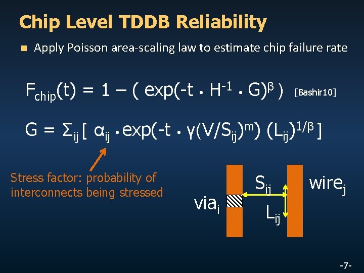
Chip Level TDDB Reliability n Apply Poisson area-scaling law to estimate chip failure rate Fchip(t) = 1 – ( exp(-t H-1 G)β ) [Bashir 10] G = Σij [ αij exp(-t γ(V/Sij)m) (Lij)1/β ] Stress factor: probability of interconnects being stressed viai Sij wirej Lij -7 -
Signal-Aware Analysis n n n Typical TDDB analysis assumes interconnects are under “DC stress” too pessimistic! Obtain stress factors by running cycle-accurate logic simulation too slow Proposed method: Use state probability from vector-less logic simulation much faster -8 -
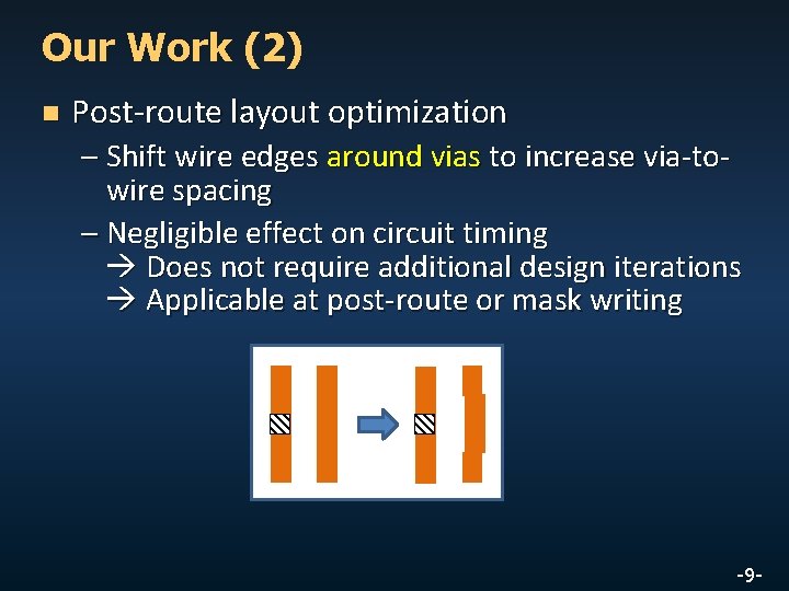
Our Work (2) n Post-route layout optimization – Shift wire edges around vias to increase via-to- wire spacing – Negligible effect on circuit timing Does not require additional design iterations Applicable at post-route or mask writing -9 -
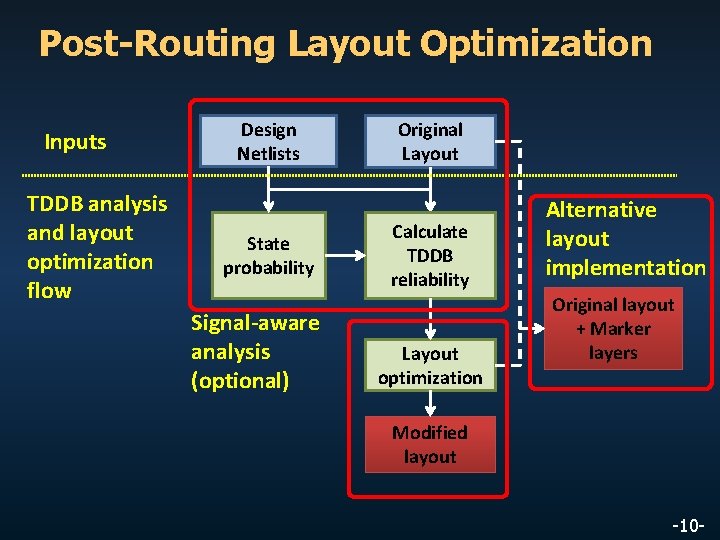
Post-Routing Layout Optimization Inputs TDDB analysis and layout optimization flow Design Netlists State probability Signal-aware analysis (optional) Original Layout Calculate TDDB reliability Layout optimization Alternative layout implementation Original layout + Marker layers Modified layout -10 -
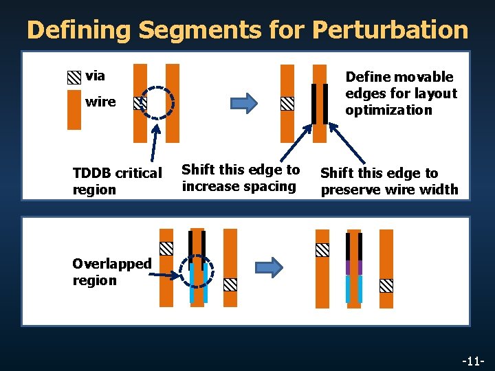
Defining Segments for Perturbation via Define movable edges for layout optimization wire TDDB critical region Shift this edge to increase spacing Shift this edge to preserve wire width Overlapped region -11 -
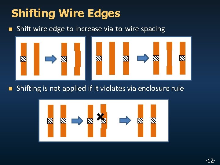
Shifting Wire Edges n Shift wire edge to increase via-to-wire spacing n Shifting is not applied if it violates via enclosure rule -12 -
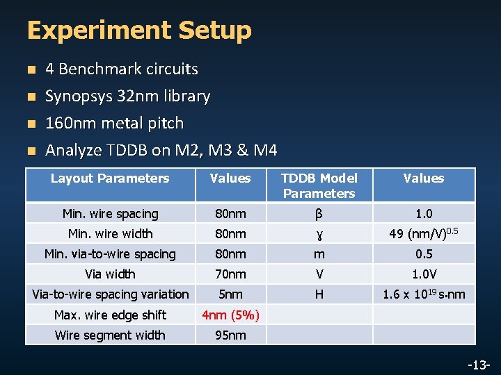
Experiment Setup n n 4 Benchmark circuits Synopsys 32 nm library 160 nm metal pitch Analyze TDDB on M 2, M 3 & M 4 Layout Parameters Values TDDB Model Parameters Values Min. wire spacing 80 nm β 1. 0 Min. wire width 80 nm ɣ 49 (nm/V)0. 5 Min. via-to-wire spacing 80 nm m 0. 5 Via width 70 nm V 1. 0 V Via-to-wire spacing variation 5 nm H 1. 6 х 1019 s nm Max. wire edge shift 4 nm (5%) Wire segment width 95 nm -13 -
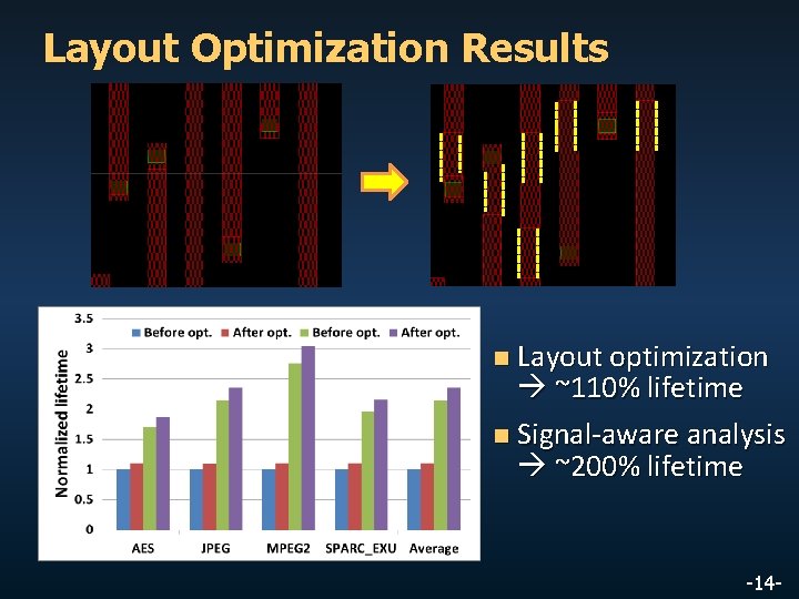
Layout Optimization Results Layout optimization ~110% lifetime n Signal-aware analysis ~200% lifetime n -14 -
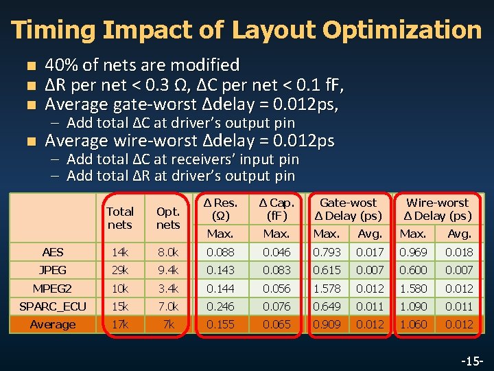
Timing Impact of Layout Optimization n 40% of nets are modified ΔR per net < 0. 3 Ω, ΔC per net < 0. 1 f. F, Average gate-worst Δdelay = 0. 012 ps, n Average wire-worst Δdelay = 0. 012 ps – Add total ΔC at driver’s output pin – Add total ΔC at receivers’ input pin – Add total ΔR at driver’s output pin Δ Res. (Ω) Δ Cap. (f. F) Max. Avg. 8. 0 k 0. 088 0. 046 0. 793 0. 017 0. 969 0. 018 29 k 9. 4 k 0. 143 0. 083 0. 615 0. 007 0. 600 0. 007 MPEG 2 10 k 3. 4 k 0. 144 0. 056 1. 578 0. 012 1. 580 0. 012 SPARC_ECU 15 k 7. 0 k 0. 246 0. 076 0. 649 0. 011 1. 090 0. 011 Average 17 k 7 k 0. 155 0. 065 0. 909 0. 012 1. 060 0. 012 Total nets Opt. nets AES 14 k JPEG Gate-wost Δ Delay (ps) Wire-worst Δ Delay (ps) -15 -
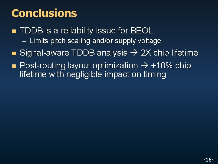
Conclusions n TDDB is a reliability issue for BEOL – Limits pitch scaling and/or supply voltage n n Signal-aware TDDB analysis 2 X chip lifetime Post-routing layout optimization +10% chip lifetime with negligible impact on timing -16 -

Thank you! -17 -
![References n n n n [Achanta 06] R. S. Achanta, J. L. Plawsky and References n n n n [Achanta 06] R. S. Achanta, J. L. Plawsky and](http://slidetodoc.com/presentation_image_h/96aa91da06062af396509690c80f7997/image-18.jpg)
References n n n n [Achanta 06] R. S. Achanta, J. L. Plawsky and W. N. Gill, "A Time Dependent Dielectric Breakdown Model for Field Accelerated Low-k Breakdown Due To Copper Ions”, AIP Applied Physics Letters 91 (23) 2006, pp. 234106 -1 - 234106 -3. [Bashir 10] M. Bashir and L. Milor, “Towards a Chip Level Reliability Simulator for Copper/Low-k Backend Processes”, IEEE Design Automation and Test in Europe, 2010, pp. 279 -282. [Berman 81] A. Berman, “Time-Zero Dielectric Reliability Test By a Ramp Method”, IEEE Intl. Reliability Physics Symposium, 1981, p. 204. [Chen 06] F. Chen, O. Bravo, K. Chanda, P. Mc. Laughlin, T. Sullivam, J. Goill, J. Lloyd, F. Kontra and J. Aitken, “Comprehensive Study of Low-k Si. COH TDDB Phenomena and Its Reliability Lifetime Model Development”, IEEE Intl. Reliability Physics Symposium, 2006, p. 46. [Lee 88] J. Lee, I. C. Chen, and C. Hu, “Modeling and Characterization of Gate Oxide Reliability”, IEEE Intl. Reliability Physics Symposium, 1988, p. 2268 -2278. [Lloyd 05] J. R. Lloyd, E. Liniger, and T. M. Shaw, “Simple model for time-dependent dielectric breakdown in inter- and intralevel low-k dielectrics”, AIP Journal of Applied Physics 98, (084109) (2005), 084109 -1 – 084109 -6. [Zhao 11] L. Zhao, Z. Tőkei, K. Croes, C. J. Wilson, M. Baklanov, G. P. Beyer, and C. Claeys, “Direct Observation of the 1/E Dependence of Time-Dependent Dielectric Breakdown in the Presence of Copper”, AIP Applied Physics Letters 98 (03) (2011), pp. 032107 -1 - 032107 -3. -18 -
- Slides: 18