POSITION SENSITIVE SEMICONDUCTOR DETECTORS QUICK FACTS Gas filled


 Detectors: •")
- Slides: 25
POSITION SENSITIVE SEMICONDUCTOR DETECTORS
QUICK FACTS • Gas filled devices can be used as position sensitive radiation detectors. • Semiconductors also have this ability! • Sometimes they’re preferred because they’re small and have a low biasvoltage. • The also have a greater stopping power, so they’re good for long range radiation!
RESISTIVE CHARGE DIVISION • Essentially made of a 1 D strip of Si or Ge. • One contact has a large series resistance. • The resistive contact is connected to ground at one end, and an amplifier at the other, which outputs the position signal.
Resistive Charge Division
EXAMPLE AND NOTES • Position resolution deteriorates as energy of the incident particle decreases. • Position resolution can be 0. 51. 0% FWHM at room temperature, for active lengths of 50 -100 mm! • This happens because the statistics depend heavily upon the number of charge carriers collected by the resistive strip. • The resistive contact is typically made by metal evaporation or ion implantation. • An example with fission fragments:
Fission Fragments
MICROSTRIP DETECTORS • Subdivide an electrode into multiple strips. • Strips are usually fabricated onto the surface by ion implantation and/or photolithography. • Electron-Hole pairs created in the volume will travel along the electric field lines to the nearest electrode segment. • Thus, strong signals will only come from segments which collected many charge carriers! • To avoid the many independent channels which would be required to measure each strip individually, a charge divider is used to find the strip closest to the interaction! • This approach can give a 10μm resolution for α-particles.
MICROSTRIP DETECTORS • A double sided detector can also be created, if one wishes to measure 2 D coordinates. • However, problems occur on the nside. The Si-Oxide layer which is meant to reduce leakage currents accumulates positive charges at the interface. • This creates a mobile layer of electrons which makes a conductive path between strips. • This problem is fixed by implementing p-type strips between the electrodes to interrupt the electron layer. • 2 D strip detectors are great for XRay imaging, and thick versions are also good for gamma rays (Compton Scattering).
2 D Strip Detector
PAD OR PIXEL DETECTORS • A brute force method of 2 D detection. • Make a checkerboard of small elements on the top electrode. • If they’re a mm or larger, it’s a pad detector. • If they’re less than a mm, you guessed it! It’s a pixel detector. • Note a connection must exist between individual electrodes and readouts. • Advantage: Small size makes for a low capacitance leakage current. • Which in turn reduces noise (considerable reduction in comparison to strip detectors)! • Individual connections to each pixel is hard to achieve. • Most commonly, it’s done with indium bond bumps.
Common Pixel Detector
SEMICONDUCTOR DRIFT DETECTORS • Interestingly enough the drift time of charge carriers can be used to deduce the position as well! • Eventually they’re transported through the potential, to the anode at the edge of the wafer. • Junctions are formed at both faces of a large wafer, each is reverse biased until the detector is fully depleted. • The time required for them to reach the anode then gives a distance between the collection point and creation point. • Electrons created are confined within a potential well, and forced to drift parallel to the wafer surface. • In the linear detector, the second coordinate is determined by segmenting the anode.
Linear Drift Detector
SEMICONDUCTOR DRIFT DETECTORS • A cylindrical detector may be used to minimize the capacitance, due to the small size of the anode. • In general, drift detectors have the advantage of improving energy resolution. • Since, electrons can be drifted over large distances and capacitance can be much smaller that other conventional detectors! • For this reason, drift detectors have gained popularity as X-Ray spectrometers.
Cylindrical Drift Detector
Cylindrical Drift Detector
CHARGE COUPLED DEVICES • Excellent for radiation detection and imaging. • Specifically, they’re great for tracking or imaging high energy minimum ionizing particles. Or, X-Ray spectroscopy, especially low energies. • Typically, a depletion region is created below the front surface, and a potential minimum a few microns below the surface (usually made of metal-oxide-silicon, MOS). • However, the MOS structure can be replaced p-n structures at the surface (Fig. 1), and in some configurations the Si substrate is only partially depleted (Fig. 2). • Other times, the Si can be fully depleted so that radiation can be incident from the back side, without attenuation occurring due to the top structures.
Charge Coupled Devices
Charge Coupled Devices
CHARGE COUPLED DEVICES • How they work: The area is divided into many small pixels through control electrodes and channel stops. • The “drive pulses” then begin to systematically fire (after the exposure time has passed). • Voltages are applied so that each pixel has it’s own potential well. • The top most right pixel is collected first, and then the adjacent pixel in that row. . . So it goes, until all pixels have been collected. • Thus, ionizing radiation created at a pixel should be confined there. • The potential wells continue to collect and hold charges over the exposure time. • Shockingly, CCD’s are very good at not losing charge!
CHARGE COUPLED DEVICES • Some quick facts: • Capacitances can be on the order of pico-Farads, meaning incredibly low noise. • Because of this low noise, CCD’s are even capable of measuring the charge generated by a single particle, or X-Ray. • Throughout the exposure time, electrons can be thermally generated (noise source), which makes it convention to cool CDC’s by 50 -100 degrees less than room temperature. • The collection period has to be much smaller than the exposure time, else smearing can occur.
Charge Coupled Devices
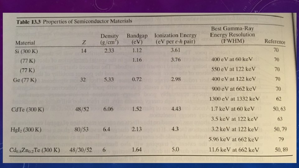
CADMIUM TELLURIDE • Some quick facts about Cd. Te Detectors: • Combines high atomic numbers (48 and 52), which a large enough band gap (1. 52 e. V) to allow for operation near room temperature. • Probability of absorption is 4 -5 times higher than in Ge, and 100 times larger than Si. • Applies best when high gamma ray detection per unit volume is required. • Usually doped purposefully with Cl to compensate for impurities and defects, making it a highly resistive p-type. • Holes have a poor collection efficiency, so energy resolution is poor compared to Ge and Si.
CADMIUM ZINC TELLURIDE • Some quick facts about Cd. Zn. Te (CZT) Detectors: • Significantly higher resistivity than regular Cd. Te. • Depending upon the blending of the elements, the bandgap energies typically range from (1. 53 -1. 64 e. V). • Gamma absorption efficiency is similar to Cd. Te, but the usual higher bandgap reduces the free carrier concentration, and thus the leakage current (compared to Cd. Te). • Of course, CZT can operate at room temperature and still has resolution “problems” when compared to Ge and Si, but usually has better resolution than Cd. Te!