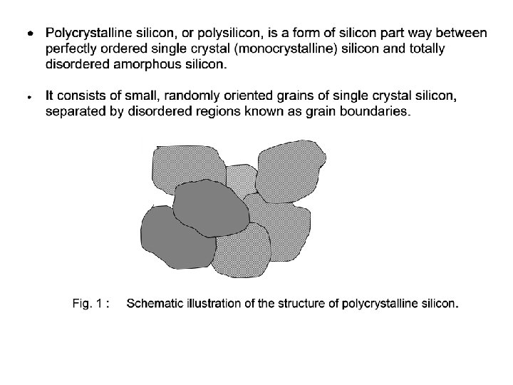
Polysilicon Emitter Bipolar Transistor In this lecture you

Polysilicon Emitter Bipolar Transistor

In this lecture, you will learn about • the structure of the polysilicon bipolar transistor • the gain mechanism of the polysilicon bipolar transistor • the spiking problem, and how to overcome it Read : 1. Neamen, “Semiconductor Physics and Devices”, 3 rd Edition, Mc. Graw. Hill, (2003), pp. 430 -431. 2. P. Ashburn, “Design and Realization of Bipolar Transistors”, Wiley, (1988), pp. 89 - 96.

interfacial oxide polysilicon emitter monocrystalline silicon emitter N+ N+ base p ITUN IRECI IREC Fig. 4 : Components of the hole current in the emitter of a polysilicon emitter transistor
")
polysilicon emitter N+ Hole Concentration single crystal silicon emitter N+ base P p. E(x) p. E 0 Depth from surface, x Fig. 3 : Hole concentration profiles in transistors with a polysilicon emitter (solid line), and without a polysilicon emitter (chain line).

In a polysilicon emitter bipolar transistor, the base current is reduced, the collector current remains unchanged. Therefore, the current gain, , is enhanced. Fig. 5 : Gummel plots of conventional bipolar transistors (solid line) and polysilicon emitter bipolar transistors (lines with circles).
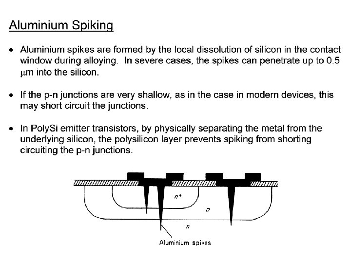

Fig. 6 : Emitter-base current, showing effect of spiking Fig. 7 : Transistor output characteristics, showing effect of spiking

Question : Conventional bipolar transistors can easily provide current gains of up to 300. This is sufficient for most applications. Even though polysilicon emitter bipolar transistors can provide higher current gains, the extra gain is not really necessary. So, what is the advantage of polysilicon emitter bipolar transistors ?
- Slides: 12