PN Junctions So far we learned the basics

P-N Junctions

• So far we learned the basics of semiconductor physics, culminating in the Minority Carrier Diffusion Equation • We now encounter our simplest electronic device, a diode • Understanding the principle requires the ability to draw band-diagrams • Making this quantitative requires ability to solve MCDE (only exponentials!) • Here we only do the equilibrium analysis

P-N junction diode I V

P-N junction diode I V I = I 0(e I p q. V/hk. T -1) 2/N ) (L /t ) = q(n 0 i D p p pn v

P-N Junctions - Equilibrium What happens when these bandstructures collide? • Fermi energy must be constant at equilibrium, so bands must bend near interface • Far from the interface, bandstructures must revert

Time < 0: Pieces separated
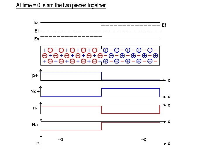

Gradients drive diffusion left

Gradients drive diffusion

++ ++ ++ + - - - But charges can’t venture too far from the interface because their Coulomb forces pull them back!

Separation of a sea of charge, leaving behind a charge depleted region http: //scott. club 365. net/uploaded_images/Moses-Parts-the-Red-Sea-2 -782619. jpg

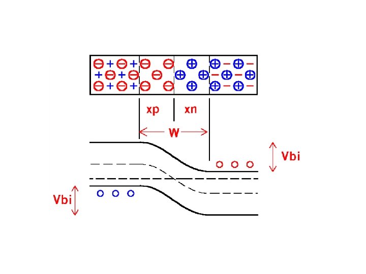
Resulting in a barrier across a depletion region

E Depletion Region E

How much is the Built-in Voltage? P side N side

How much is the Built-in Voltage? Na acceptor level on the p side Nd donor level on the n side

Special case: One-sided Junctions • One side very heavily doped so that Fermi level is at band edge. • e. g. p+-n junction (heavy B implant into lightly doped substrate)

How wide is the depletion region?

Depletion Approximation-step junction x

Depletion approximation-step junction Exponentials replaced with step-functions
 Kse 0")
Doping N A xp = N D xn = WD/(NA-1 + ND-1) Kse 0 Em = -q. NAxp = -q. NDxn = -q. WD/(NA-1 + ND-1) Vbi = ½|Em|WD Charge Density Electric Field Electrostatic Potential

Depletion Width
")
Maximum Field Em = 2 q. Vbi/kse 0(NA-1+ND-1)

How far does Wd extend into each junction? Depletion width on the n-side depends on the doping on the p-side Depletion width on the p-side depends on the doping on the n-side e. g. if NA>>ND then xn>>xp One-sided junction


P-N Junction with applied voltage

Reverse Bias • +Voltage to the n side and –Voltage to the p side: Depletion region will be larger

Reverse Bias Band Diagram

Reverse Bias depletion Applied voltage disturbs equilibrium EF no longer constant Reverse bias adds to the effect of built-in voltage

Forward Bias + - Negative voltage to n side positive to p side More electrons supplied to n, more holes to p Depletion region gets smaller

Forward Bias Depletion

General Expression • Convention = Vappl= + forward bias Vappl= - for reverse bias

Positive voltage pulls bands down- bands are plots of electron energy Fp Fn n = nie(Fn-Ei)/k. T p = nie(Ei-Fp)/k. T Fermi level is not constant Current Flow

In summary A p-n junction at equilibrium sees a depletion width and a built-in potential barrier. Their values depend on the individual doping concentrations Forward biasing the junction shrinks the depletion width and the barrier, allowing thermionic emission and higher current. The current is driven by the splitting of the quasi-Fermi levels Reverse biasing the junction extends the depletion width and the barrier, cutting off current and creating a strong I-V asymmetry In the next lecture, we’ll make this analysis quantitative by solving the MCDE with suitable boundary conditions
- Slides: 34