Plug In Card with Commercial Buck Converters Satish

Plug In Card with Commercial Buck Converters Satish Dhawan, Oliver Baker, Hunter Smith, Paul Tipton, Yale University Hucheng Chen, James Kierstead, David Lynn, Sergio Rescia, BNL Marc Weber, RAL Chris Musso, Allen Mincer NYU ATLAS Tracker Upgrade Workshop, Amsterdam 03 - 07 November, 2008

Requirements Voltage Ratio > 8 For Good Efficiency Iout >3 amps Air Coil / Magnetics Radiation Hardness Vin = 2. 5 – 17 V GND Enable Power Good Load 0. 25 µm Technology Test ASIC 2. 5 V @ ~ 3 amps 0. 13 µm Technology ASIC 1. 3 V @ ST 1 S 10 Max 8654 Monolithic Commercial Converters 18 V 3 amps 12 V 8 amps Following To be available early in 2009 ST L 5988 TI TPS 54620 AD 21 xx National Enpirion 29 October, 08 18 V 4 amps 17 V 6 amps 20 V 3 amps 12 V 6 amps 0. 35 µm BCD 0. 35 µm CMOS 0. 25 µm CMOS Plug in Card – Power Vout = 2. 5 / 1. 3 V Small Plug-in Card GND

Silicon Chip Size 0. 3 x 0. 3 cm 3 Sizes of Spiral Coils Coil with Ferrite

Buck Converter Noise Pick-up with Vin / Vout > 8 Previously studies done with Vin ~ 5. 5 V 17 V 5 V 30 mΩ Switch Enable 20 mΩ Switch Power Good PWM Controller : Low Voltage High Voltage: On Switches- LDMOS, Drain Extension, Deep Diffusion etc

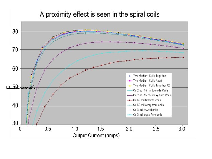
Proximity Effect Large Coils For Larger Inductance connect coils in series Medium Coils Coil Spacing Far – 1. 5” Near – 0. 006” Touching – <0. 001” L R L R 100 k. Hz 0. 976 μH 0. 183 Ω 1. 751 μH 0. 184 Ω 2. 150 μH 0. 185 Ω 2 oz copper for coils, 6 mill spacing with Kapton LCR Meter of Teaching Lab Calibrator disappeared !!!

Not Enough Inductance

Vin / Vout = 4. 3

SOC Package Version of Plug in Cards 1. Coil: magnetic / Air Plug-in Card 2. Heat Removal Comment Coil 3. Pin. High Voltage Ratio 33, 35, 37, 39 Digital Power In SILICON 4. 34, 36, 38, 40 Al Power Conductors Digital Return (Hybrid Ground) 41, 43 42, 44 45 52 Connector Auxiliary Analogue Power In Auxiliary Analogue Return HVRet HV (Sensor Bias) Shirking of Power Packages by 3 D Goal A Component that can be wire bonded To Hybrid ( Like ABCD Chips) Size= 10 x 10 mm or Smaller

EN 5365 Korean Foundry EN 5360 IHP Foundry Both are can be used for Space Applications IHP Foundry for HEP
 03 November 2008 Aachen (Lutz Feld +3) + Yale")
Visit IHP Microelectronics, Frankfurt (Oder) 03 November 2008 Aachen (Lutz Feld +3) + Yale (Satish Dhawan) IHP v Prof Bernd Tillack- Deputy Scientific Director v Dieter Knoll – Technology Head v Roland Sorge – Device Engineer v Ulrich Jagdhold Systems Engineer Ø 85 % Public Funds 250 people. 50 Wafers / week. Capacity 150 Wafers Ø Up to 80 GHz Circuits Ø Try to understand why Hard IHP made devices are Radiation Ø LDMOS Lateral Diffused MOS Transistor Switches. Use N & P Channel Ø Sending above Devices for Radiation Testing Ø Developing New Device Structure for 12 Volts Ø 0. 25 m Technology Ø Test New LDMOS Devices with Buck Controller

Lonely @ Top of the World The End
- Slides: 12