PLT 206 Microcontroller Systems CCP PIC 16 Timer



- Slides: 49

PLT 206 Microcontroller Systems CCP PIC 16 Timer Programming in Hitech-C 1

Today’s Lecture List the CCP module/s of PIC 16 and their associated registers. Describe the various modes of the PIC 16 CCP module. Program the PIC 16 CCP module in ‘Hitech C’. 2

Introduction Stands for Capture/Compare/PWM. Allows the user to time and control different events. The (CCP) module is a programmable software able to operate in one of the three modes: A Capture input A Compare output A Pulse Width Modulation (PWM). 3

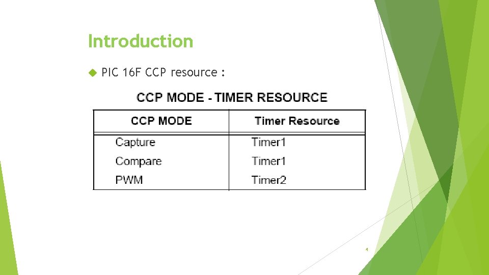
Introduction PIC 16 F CCP resource : 4

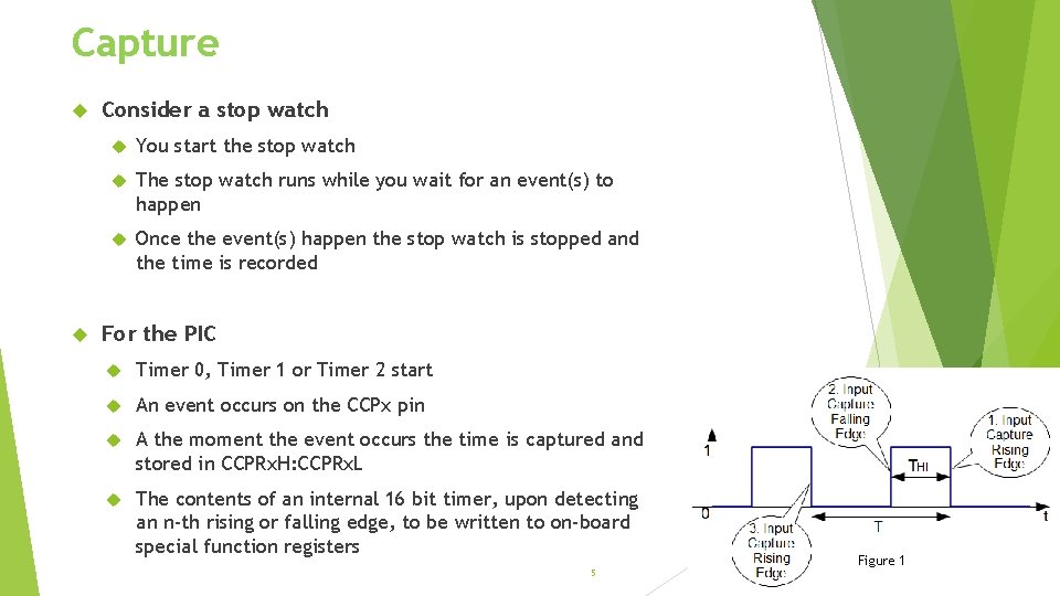
Capture Consider a stop watch You start the stop watch The stop watch runs while you wait for an event(s) to happen Once the event(s) happen the stop watch is stopped and the time is recorded For the PIC Timer 0, Timer 1 or Timer 2 start An event occurs on the CCPx pin A the moment the event occurs the time is captured and stored in CCPRx. H: CCPRx. L The contents of an internal 16 bit timer, upon detecting an n-th rising or falling edge, to be written to on-board special function registers 5 Figure 1

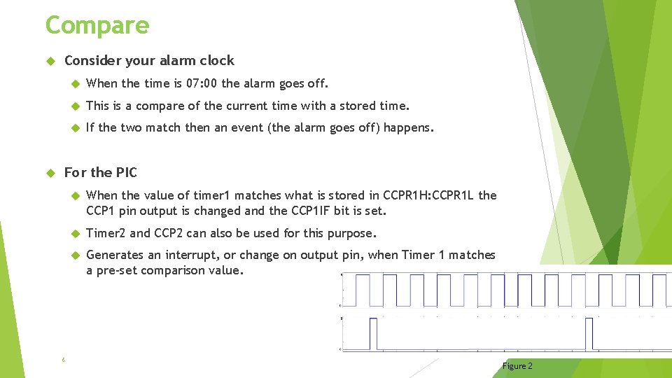
Compare Consider your alarm clock When the time is 07: 00 the alarm goes off. This is a compare of the current time with a stored time. If the two match then an event (the alarm goes off) happens. For the PIC 6 When the value of timer 1 matches what is stored in CCPR 1 H: CCPR 1 L the CCP 1 pin output is changed and the CCP 1 IF bit is set. Timer 2 and CCP 2 can also be used for this purpose. Generates an interrupt, or change on output pin, when Timer 1 matches a pre-set comparison value. Figure 2

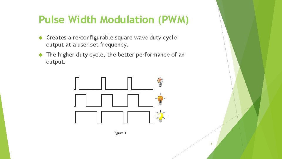
Pulse Width Modulation (PWM) Creates a re-configurable square wave duty cycle output at a user set frequency. The higher duty cycle, the better performance of an output. Figure 3 7

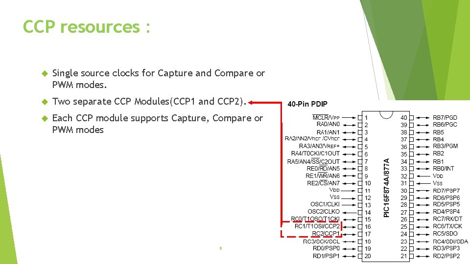
CCP resources : Single source clocks for Capture and Compare or PWM modes. Two separate CCP Modules(CCP 1 and CCP 2). Each CCP module supports Capture, Compare or PWM modes 8

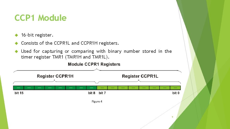
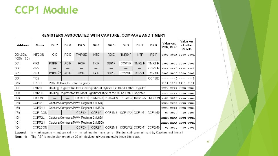
CCP 1 Module 16 -bit register. Consists of the CCPR 1 L and CCPR 1 H registers. Used for capturing or comparing with binary number stored in the timer register TMR 1 (TMR 1 H and TMR 1 L). Figure 4 9

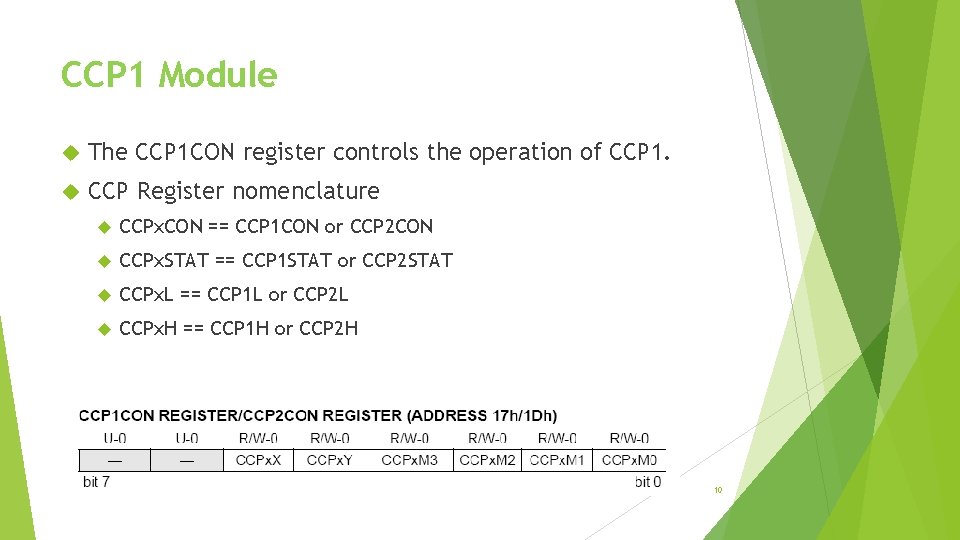
CCP 1 Module The CCP 1 CON register controls the operation of CCP 1. CCP Register nomenclature CCPx. CON == CCP 1 CON or CCP 2 CON CCPx. STAT == CCP 1 STAT or CCP 2 STAT CCPx. L == CCP 1 L or CCP 2 L CCPx. H == CCP 1 H or CCP 2 H 10

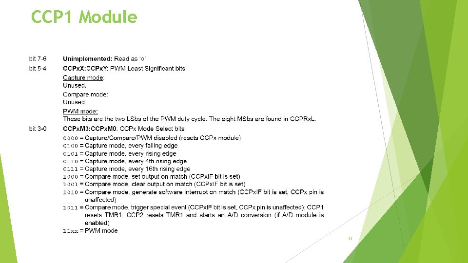
CCP 1 Module 11

CCP 1 Module 12

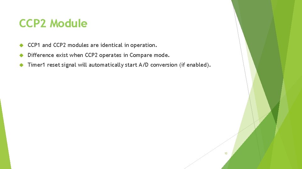
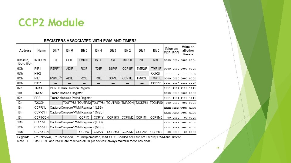
CCP 2 Module CCP 1 and CCP 2 modules are identical in operation. Difference exist when CCP 2 operates in Compare mode. Timer 1 reset signal will automatically start A/D conversion (if enabled). 13

CCP 2 Module 14

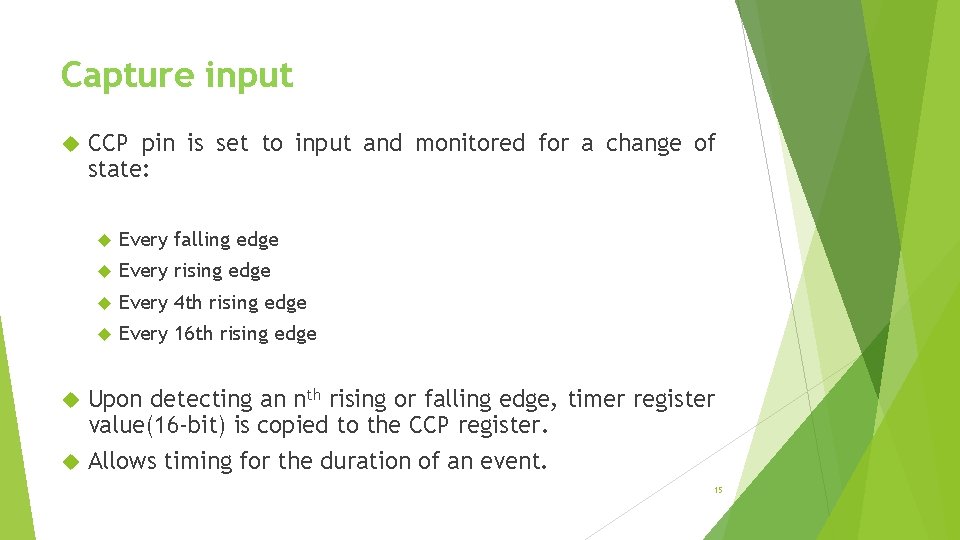
Capture input CCP pin is set to input and monitored for a change of state: Every falling edge Every rising edge Every 4 th rising edge Every 16 th rising edge Upon detecting an nth rising or falling edge, timer register value(16 -bit) is copied to the CCP register. Allows timing for the duration of an event. 15

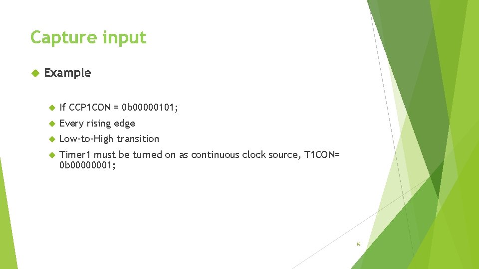
Capture input Example If CCP 1 CON = 0 b 00000101; Every rising edge Low-to-High transition Timer 1 must be turned on as continuous clock source, T 1 CON= 0 b 00000001; 16

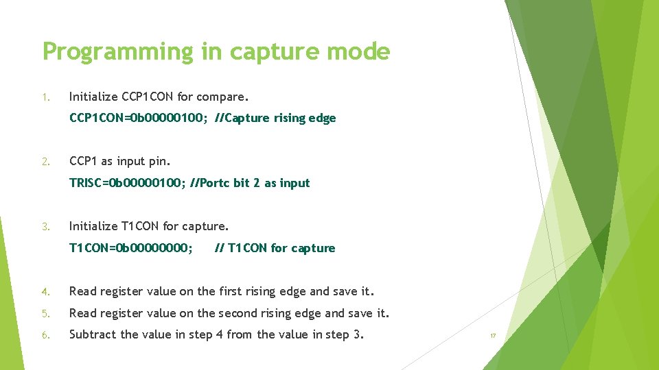
Programming in capture mode 1. Initialize CCP 1 CON for compare. CCP 1 CON=0 b 00000100; //Capture rising edge 2. CCP 1 as input pin. TRISC=0 b 00000100; //Portc bit 2 as input 3. Initialize T 1 CON for capture. T 1 CON=0 b 0000; // T 1 CON for capture 4. Read register value on the first rising edge and save it. 5. Read register value on the second rising edge and save it. 6. Subtract the value in step 4 from the value in step 3. 17

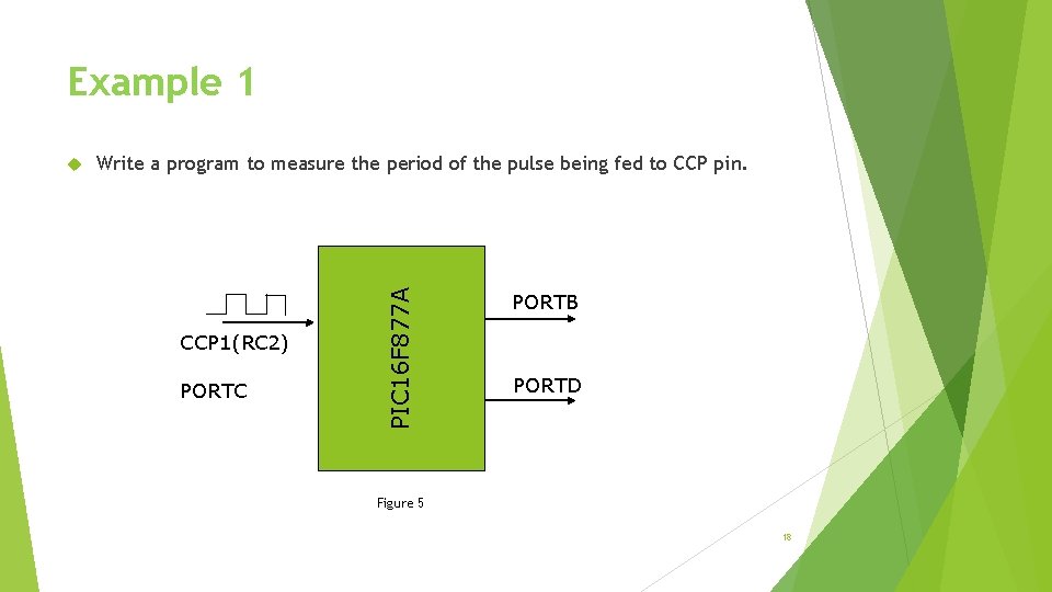
Example 1 Write a program to measure the period of the pulse being fed to CCP pin. CCP 1(RC 2) PORTC PIC 16 F 877 A PORTB PORTD Figure 5 18

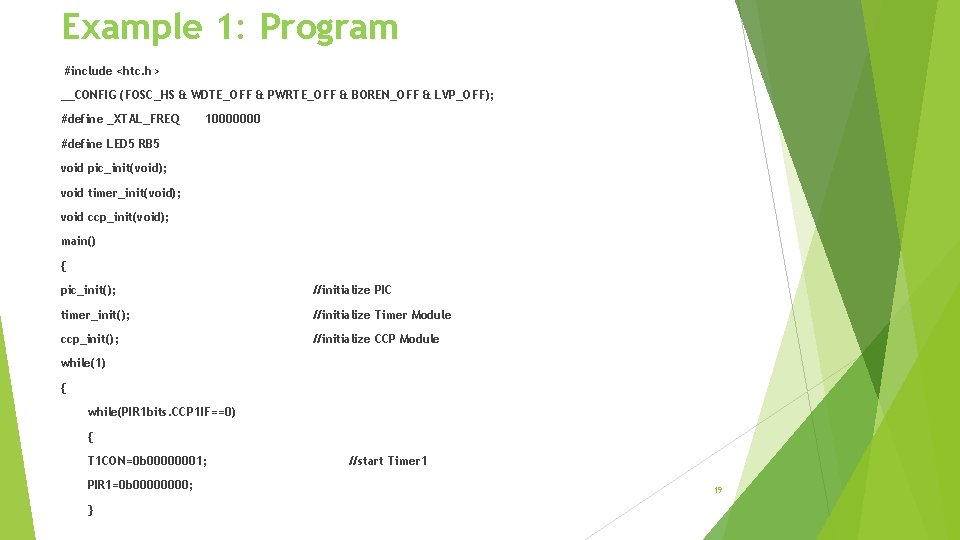
Example 1: Program #include <htc. h> __CONFIG (FOSC_HS & WDTE_OFF & PWRTE_OFF & BOREN_OFF & LVP_OFF); #define _XTAL_FREQ 10000000 #define LED 5 RB 5 void pic_init(void); void timer_init(void); void ccp_init(void); main() { pic_init(); //initialize PIC timer_init(); //initialize Timer Module ccp_init(); //initialize CCP Module while(1) { while(PIR 1 bits. CCP 1 IF==0) { T 1 CON=0 b 00000001; PIR 1=0 b 0000; } //start Timer 1 19

Example 1: Program while(PIR 1 bits. CCP 1 IF==1) { T 1 CON=0 b 0000; //stop Timer 1 PIR 1 bits. CCP 1 IF=0; PORTB=CCPR 1 L; PORTD=CCPR 1 H; } } } void pic_init(void) { TRISB=0 b 0000; PORTB=0 b 0000; TRISC=0 b 1111; PORTC=0 b 0000; TRISD=0 b 0000; PORTD=0 b 0000; } 20

Example 1: Program void timer_init(void) { T 1 CON=0 b 0000; PIR 1=0 b 0000; TMR 1 H=0; TMR 1 L=0; } void ccp_init(void) { CCP 1 CON=0 b 00000100; //Capture rising edge CCPR 1 H=0; CCPR 1 L=0; } 21

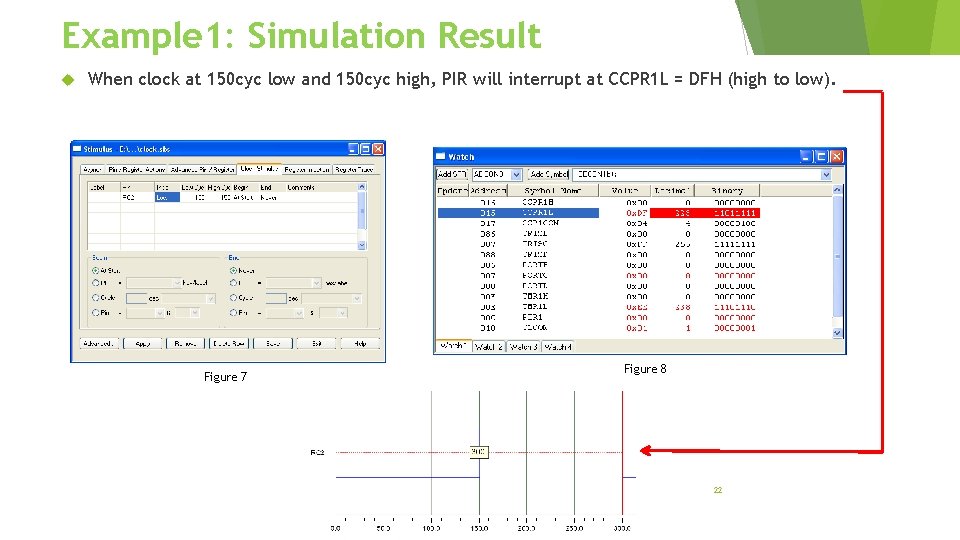
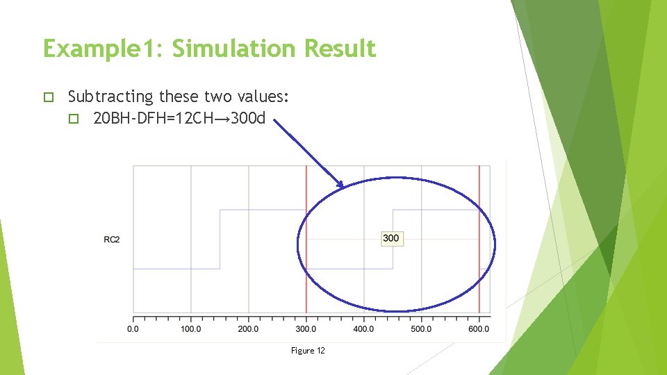
Example 1: Simulation Result When clock at 150 cyc low and 150 cyc high, PIR will interrupt at CCPR 1 L = DFH (high to low). Figure 7 Figure 8 22

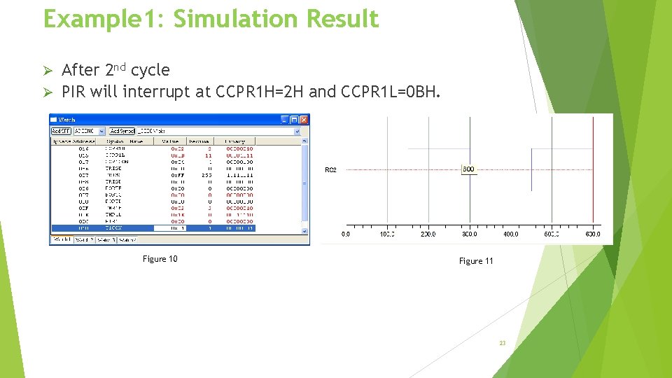
Example 1: Simulation Result After 2 nd cycle Ø PIR will interrupt at CCPR 1 H=2 H and CCPR 1 L=0 BH. Ø Figure 10 Figure 11 23

Example 1: Simulation Result o Subtracting these two values: o 20 BH-DFH=12 CH→ 300 d 24 Figure 12

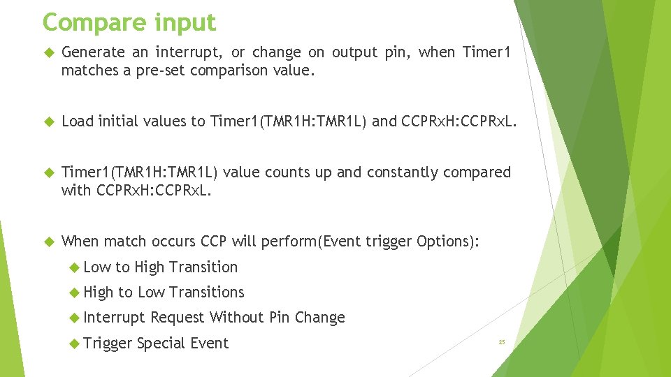
Compare input Generate an interrupt, or change on output pin, when Timer 1 matches a pre-set comparison value. Load initial values to Timer 1(TMR 1 H: TMR 1 L) and CCPRx. H: CCPRx. L. Timer 1(TMR 1 H: TMR 1 L) value counts up and constantly compared with CCPRx. H: CCPRx. L. When match occurs CCP will perform(Event trigger Options): Low to High Transition High to Low Transitions Interrupt Trigger Request Without Pin Change Special Event 25

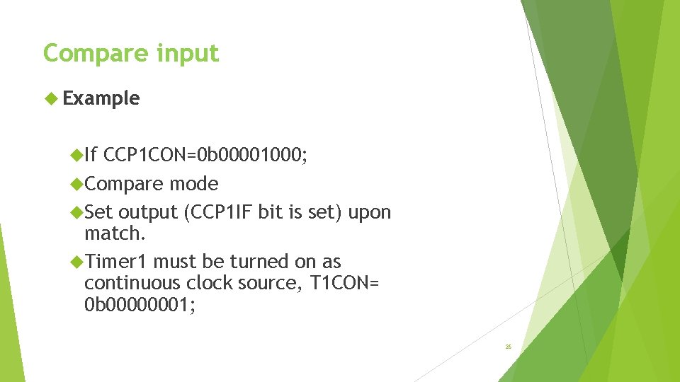
Compare input Example If CCP 1 CON=0 b 00001000; Compare mode Set output (CCP 1 IF bit is set) upon match. Timer 1 must be turned on as continuous clock source, T 1 CON= 0 b 00000001; 26

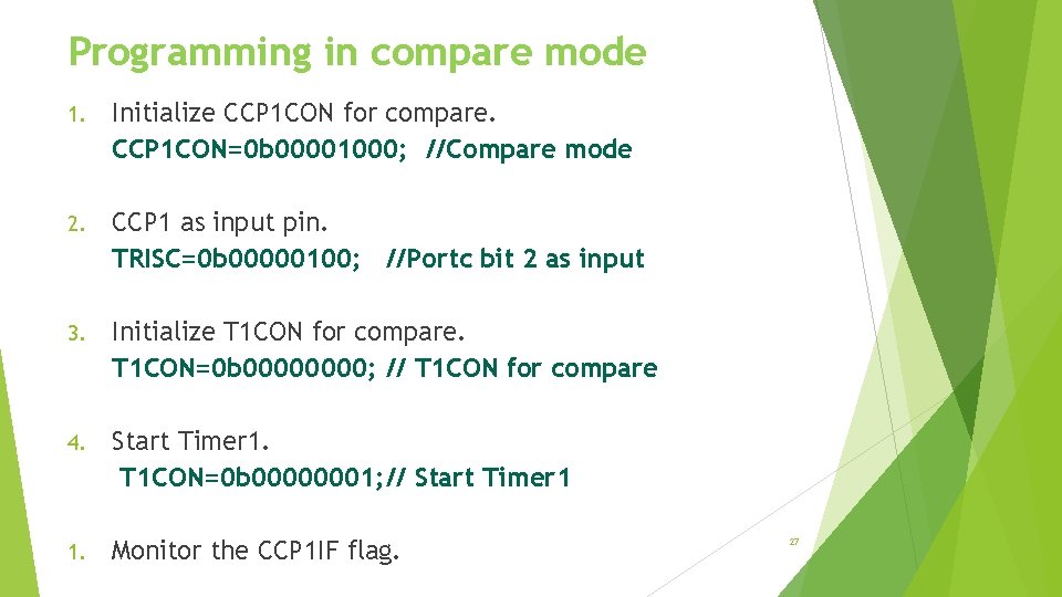
Programming in compare mode 1. Initialize CCP 1 CON for compare. CCP 1 CON=0 b 00001000; //Compare mode 2. CCP 1 as input pin. TRISC=0 b 00000100; //Portc bit 2 as input 3. Initialize T 1 CON for compare. T 1 CON=0 b 0000; // T 1 CON for compare 4. Start Timer 1. T 1 CON=0 b 00000001; // Start Timer 1 1. Monitor the CCP 1 IF flag. 27

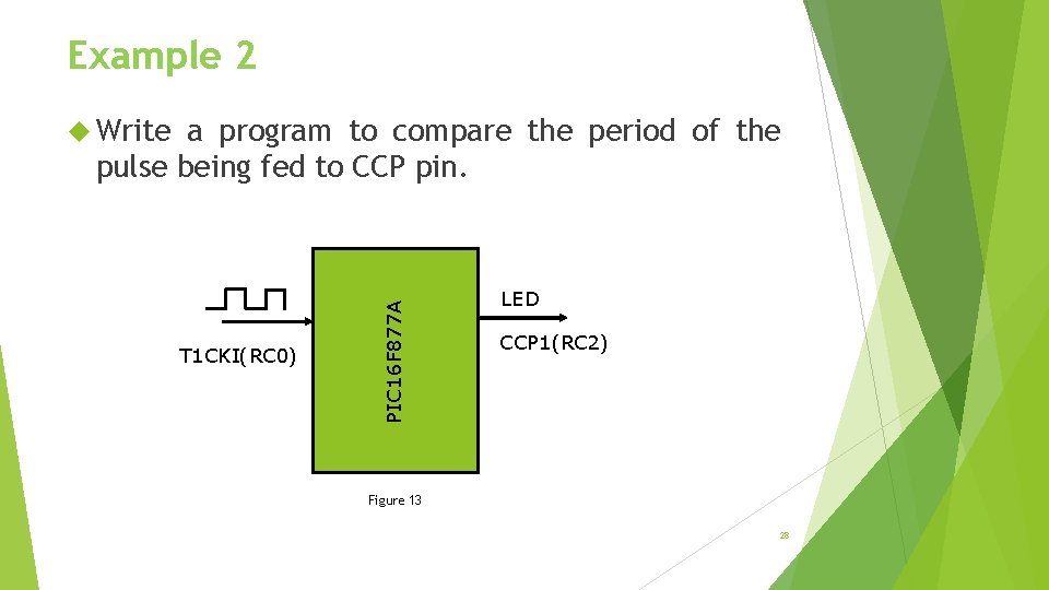
Example 2 a program to compare the period of the pulse being fed to CCP pin. T 1 CKI(RC 0) PIC 16 F 877 A Write LED CCP 1(RC 2) Figure 13 28

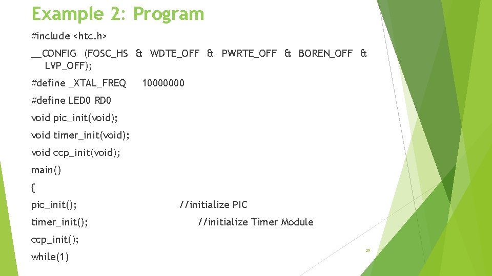
Example 2: Program #include <htc. h> __CONFIG (FOSC_HS & WDTE_OFF & PWRTE_OFF & BOREN_OFF & LVP_OFF); #define _XTAL_FREQ 10000000 #define LED 0 RD 0 void pic_init(void); void timer_init(void); void ccp_init(void); main() { pic_init(); timer_init(); //initialize PIC //initialize Timer Module ccp_init(); while(1) 29

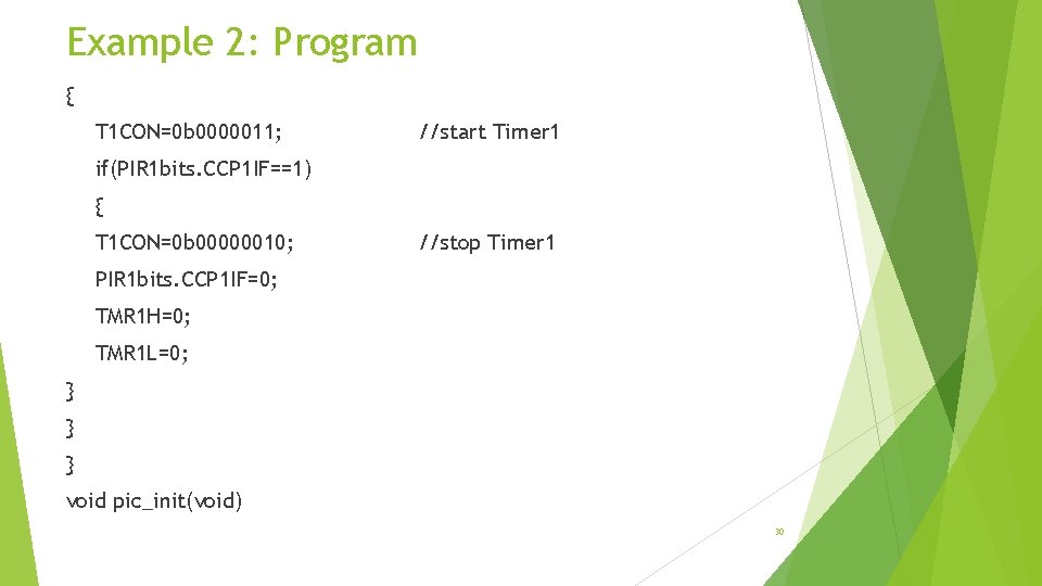
Example 2: Program { T 1 CON=0 b 0000011; //start Timer 1 if(PIR 1 bits. CCP 1 IF==1) { T 1 CON=0 b 00000010; //stop Timer 1 PIR 1 bits. CCP 1 IF=0; TMR 1 H=0; TMR 1 L=0; } } } void pic_init(void) 30

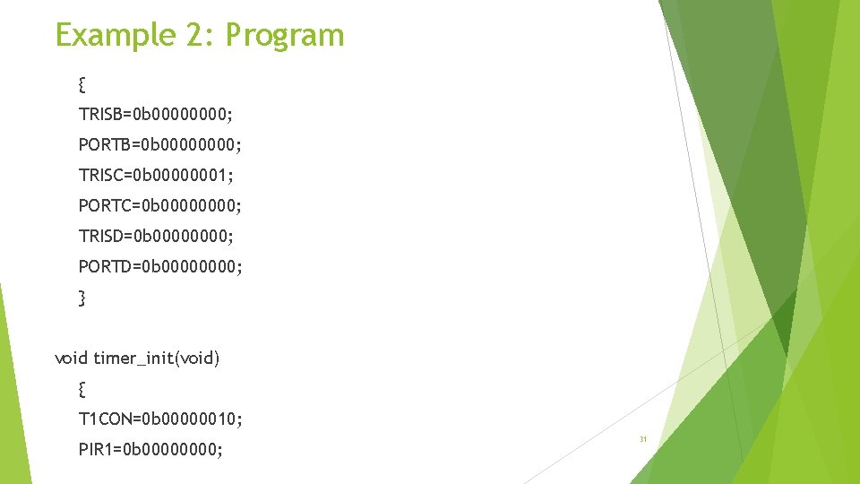
Example 2: Program { TRISB=0 b 0000; PORTB=0 b 0000; TRISC=0 b 00000001; PORTC=0 b 0000; TRISD=0 b 0000; PORTD=0 b 0000; } void timer_init(void) { T 1 CON=0 b 00000010; PIR 1=0 b 0000; 31

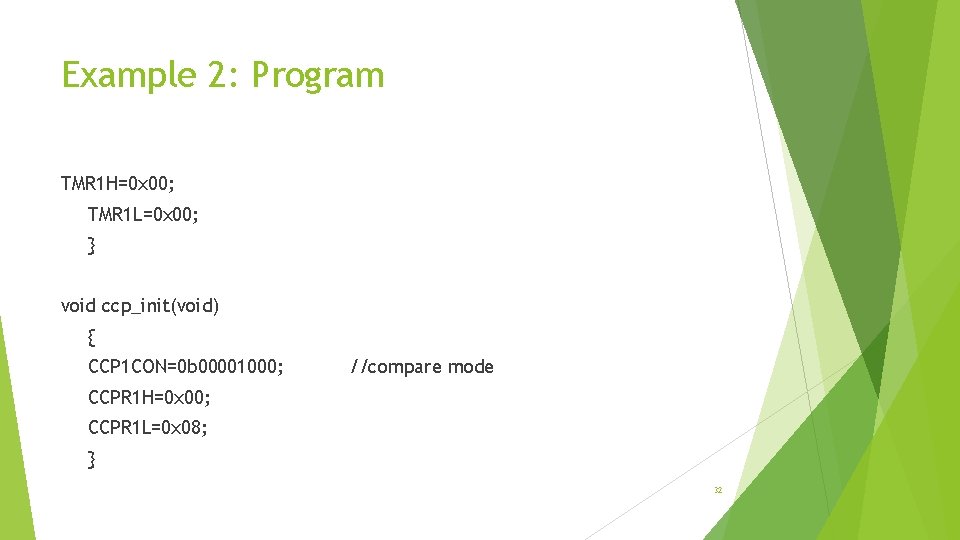
Example 2: Program TMR 1 H=0 x 00; TMR 1 L=0 x 00; } void ccp_init(void) { CCP 1 CON=0 b 00001000; //compare mode CCPR 1 H=0 x 00; CCPR 1 L=0 x 08; } 32

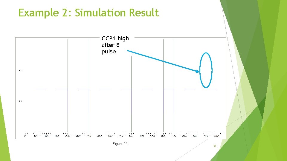
Example 2: Simulation Result CCP 1 high after 8 pulse Figure 14 33

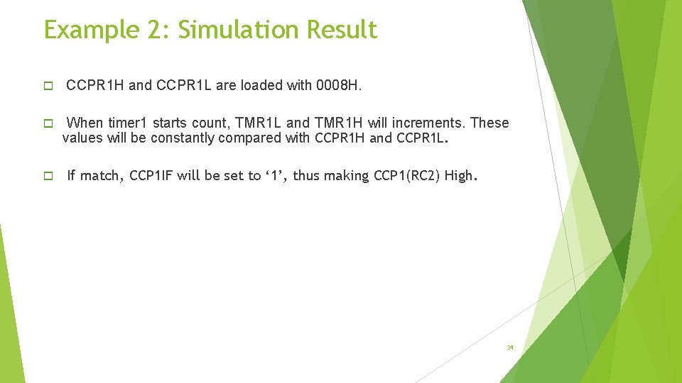
Example 2: Simulation Result o o o CCPR 1 H and CCPR 1 L are loaded with 0008 H. When timer 1 starts count, TMR 1 L and TMR 1 H will increments. These values will be constantly compared with CCPR 1 H and CCPR 1 L. If match, CCP 1 IF will be set to ‘ 1’, thus making CCP 1(RC 2) High. 34

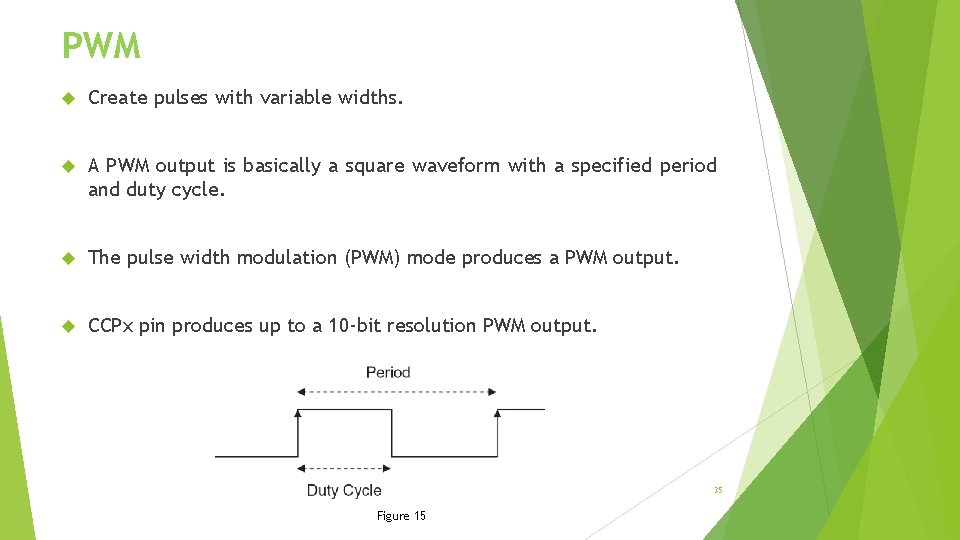
PWM Create pulses with variable widths. A PWM output is basically a square waveform with a specified period and duty cycle. The pulse width modulation (PWM) mode produces a PWM output. CCPx pin produces up to a 10 -bit resolution PWM output. 35 Figure 15

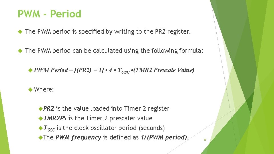
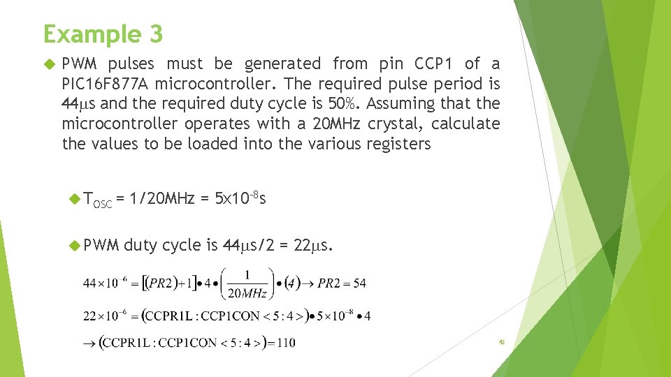
PWM - Period The PWM period is specified by writing to the PR 2 register. The PWM period can be calculated using the following formula: PWM Period = [(PR 2) + 1] • 4 • TOSC • (TMR 2 Prescale Value) Where: PR 2 is the value loaded into Timer 2 register TMR 2 PS is the Timer 2 prescaler value TOSC is the clock oscillator period (seconds) The PWM frequency is defined as 1/(PWM period). 36

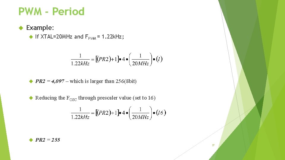
PWM - Period Example: If XTAL=20 MHz and FPWM = 1. 22 k. Hz; PR 2 = 4, 097 – which is larger than 256(8 bit) Reducing the FOSC through prescaler value (set to 16) PR 2 = 255 37

PWM - Duty Cycle Portion of pulse that stays HIGH relative to the entire period. Supports up to 10 bit resolution. CCPx pin TRIS bit must be cleared to configure the pin as output. PWM mode is enabled by placing CCPx. M 3: CCPx. M 0 = b’ 11 xx. Specified by writing to the CCPR 1 L register and to the CCP 1 CON<5: 4> bits. The CCPR 1 L contains the eight LSbs and the CCP 1 CON<5: 4> contains the two MSbs. 38

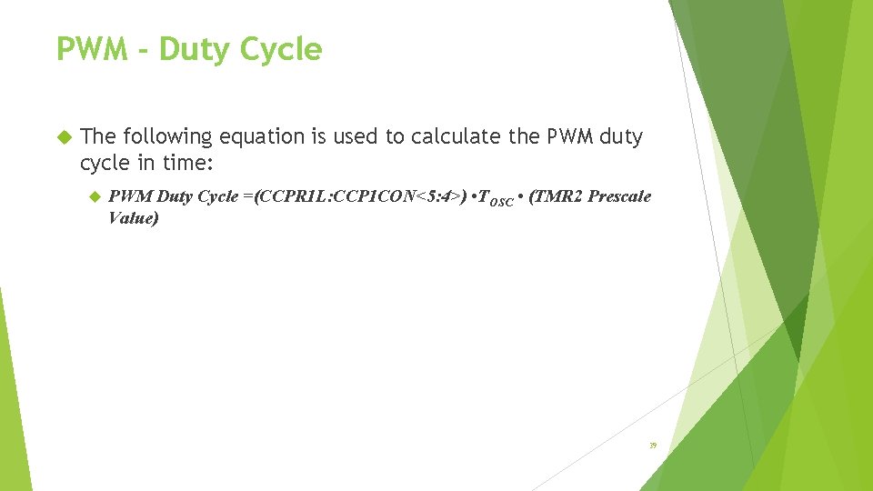
PWM - Duty Cycle The following equation is used to calculate the PWM duty cycle in time: PWM Duty Cycle =(CCPR 1 L: CCP 1 CON<5: 4>) • TOSC • (TMR 2 Prescale Value) 39

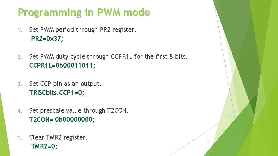
Programming in PWM mode 1. Set PWM period through PR 2 register. PR 2=0 x 37; 2. Set PWM duty cycle through CCPR 1 L for the first 8 -bits. CCPR 1 L=0 b 00011011; 3. Set CCP pin as an output. TRISCbits. CCP 1=0; 4. Set prescale value through T 2 CON= 0 b 0000; 1. Clear TMR 2 register. TMR 2=0; 40

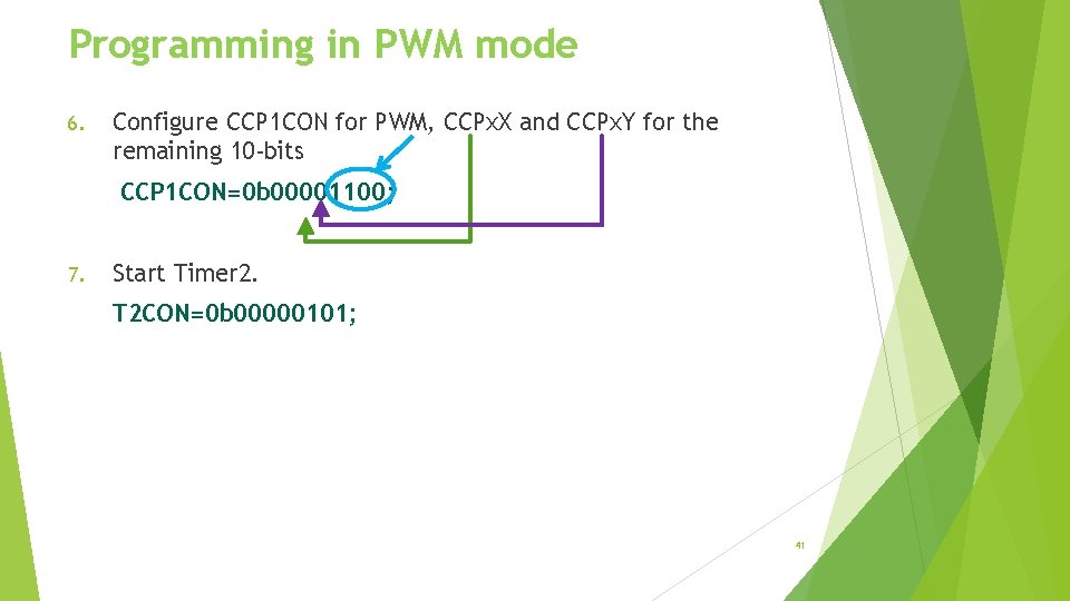
Programming in PWM mode 6. Configure CCP 1 CON for PWM, CCPx. X and CCPx. Y for the remaining 10 -bits CCP 1 CON=0 b 00001100; 7. Start Timer 2. T 2 CON=0 b 00000101; 41

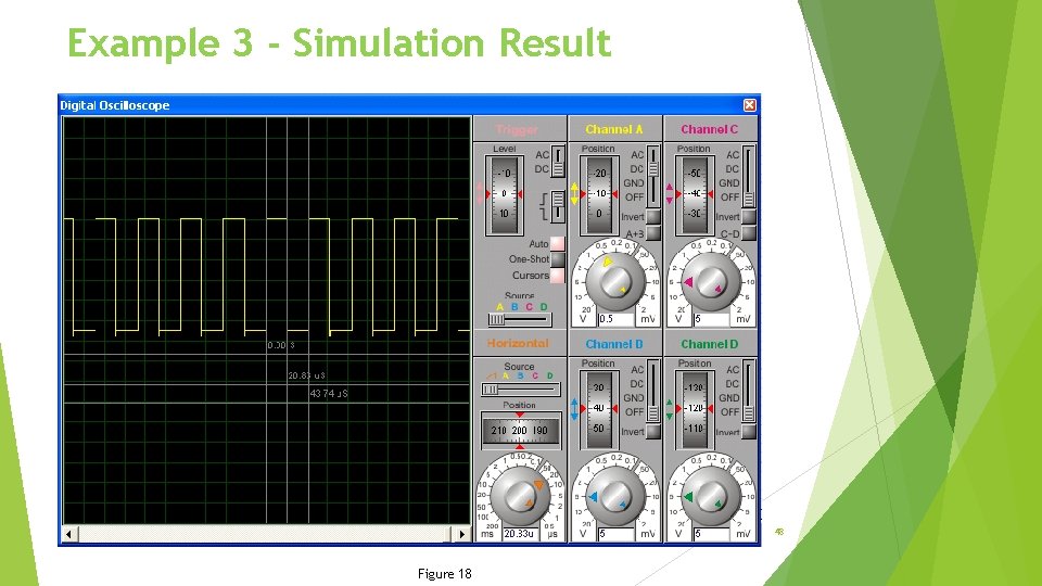
Example 3 PWM pulses must be generated from pin CCP 1 of a PIC 16 F 877 A microcontroller. The required pulse period is 44 s and the required duty cycle is 50%. Assuming that the microcontroller operates with a 20 MHz crystal, calculate the values to be loaded into the various registers TOSC = PWM 1/20 MHz = 5 x 10 -8 s duty cycle is 44 s/2 = 22 s. 42

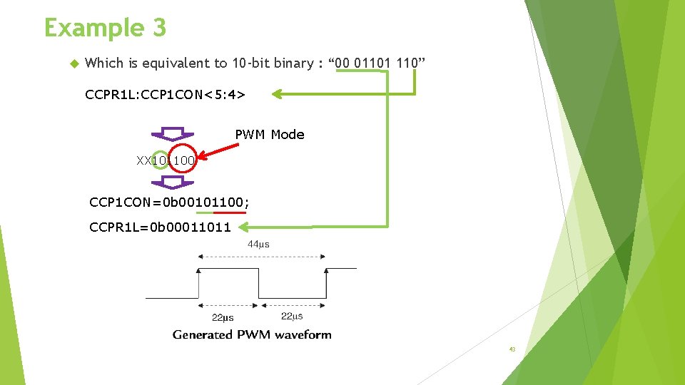
Example 3 Which is equivalent to 10 -bit binary : “ 00 01101 110” CCPR 1 L: CCP 1 CON<5: 4> PWM Mode XX 101100 CCP 1 CON=0 b 00101100; CCPR 1 L=0 b 00011011 43

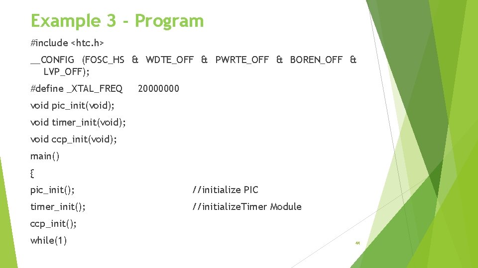
Example 3 - Program #include <htc. h> __CONFIG (FOSC_HS & WDTE_OFF & PWRTE_OFF & BOREN_OFF & LVP_OFF); #define _XTAL_FREQ 20000000 void pic_init(void); void timer_init(void); void ccp_init(void); main() { pic_init(); //initialize PIC timer_init(); //initialize. Timer Module ccp_init(); while(1) 44

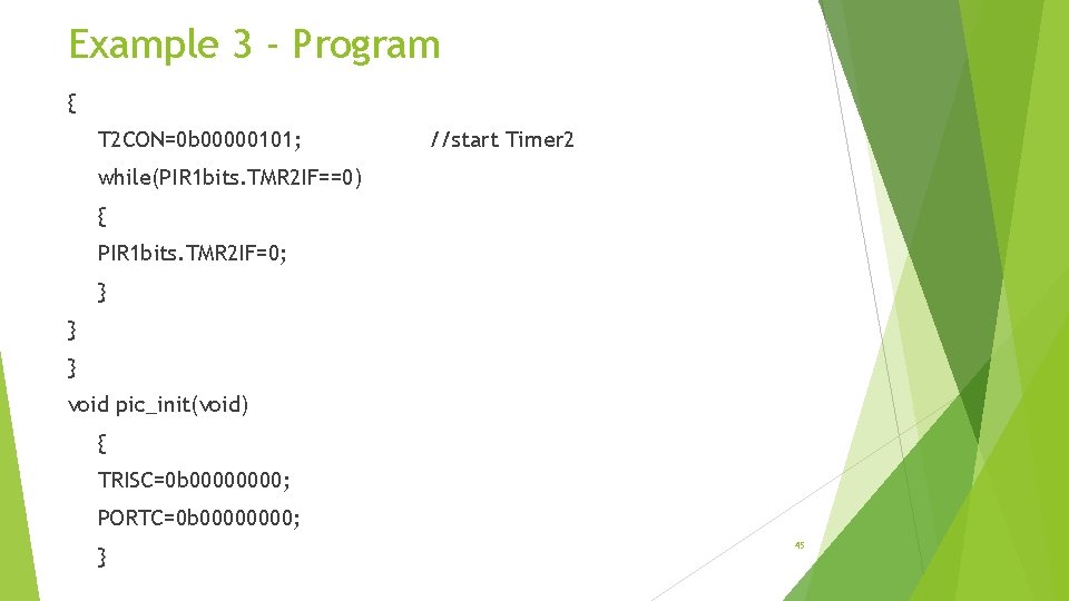
Example 3 - Program { T 2 CON=0 b 00000101; //start Timer 2 while(PIR 1 bits. TMR 2 IF==0) { PIR 1 bits. TMR 2 IF=0; } } } void pic_init(void) { TRISC=0 b 0000; PORTC=0 b 0000; } 45

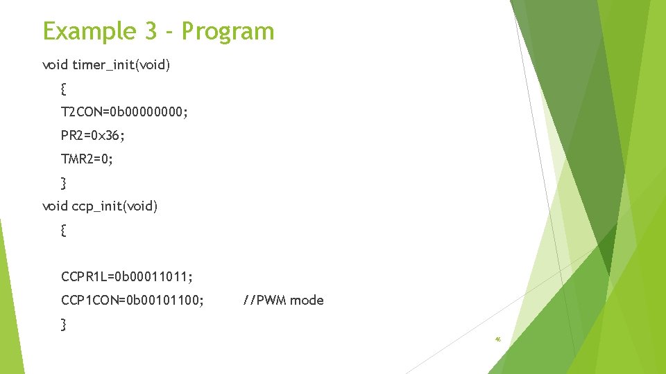
Example 3 - Program void timer_init(void) { T 2 CON=0 b 0000; PR 2=0 x 36; TMR 2=0; } void ccp_init(void) { CCPR 1 L=0 b 00011011; CCP 1 CON=0 b 00101100; //PWM mode } 46

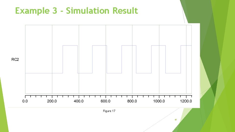
Example 3 - Simulation Result Figure 17 47

Example 3 - Simulation Result 48 Figure 18

References PIC 16 F 87 XA Data Sheet, Microchip Technology Incorporated, 2003. PIC Microcontroller And Embedded Systems: using Assembly and C for PIC 18, M. Mazidi, R. Mc. Kinlay and D. Causey, Prentice Fall, 2008. Advanced Pic Micro Controller Projects in c: From Usb to Rtos With the Pic 18 f Series, Dogan Ibrahim, Elsevier Ltd, 2008. 49