PLT 106 DIGITAL ELECTRONICS CHAPTER 5 BASIC COMBINATIONAL
PLT 106 DIGITAL ELECTRONICS CHAPTER 5: BASIC COMBINATIONAL LOGIC GATE By MDM NUR IRWANY BINTI AHMAD irwany@unimap. edu. my
DEFINITION PLT 106 DIGITAL ELECTRONICS • Combination of basic gates to form circuits that can carry out a desired application. • In combinational logic, the output level is at all times dependent on the combination of input levels. • Combinational logic circuits contain no memory (no ability to store information). 2
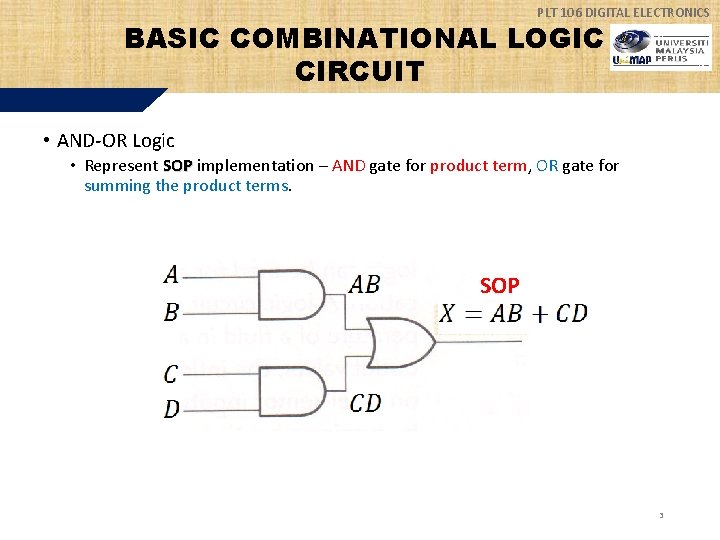
PLT 106 DIGITAL ELECTRONICS BASIC COMBINATIONAL LOGIC CIRCUIT • AND-OR Logic • Represent SOP implementation – AND gate for product term, OR gate for summing the product terms. SOP 3
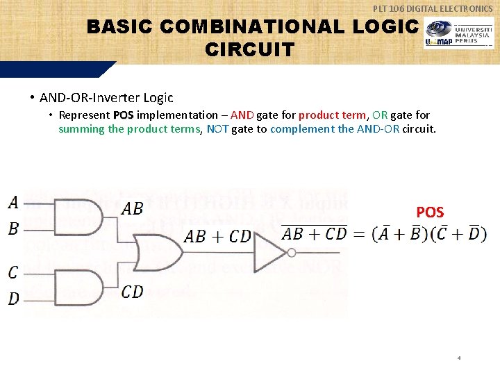
PLT 106 DIGITAL ELECTRONICS BASIC COMBINATIONAL LOGIC CIRCUIT • AND-OR-Inverter Logic • Represent POS implementation – AND gate for product term, OR gate for summing the product terms, NOT gate to complement the AND-OR circuit. POS 4
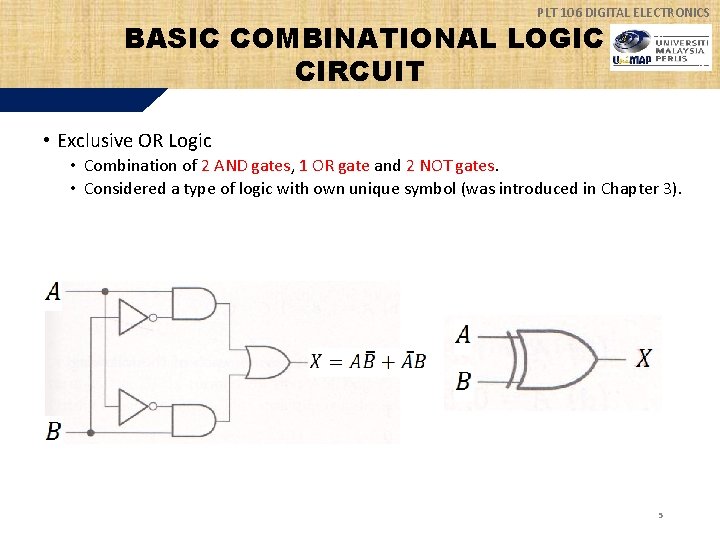
PLT 106 DIGITAL ELECTRONICS BASIC COMBINATIONAL LOGIC CIRCUIT • Exclusive OR Logic • Combination of 2 AND gates, 1 OR gate and 2 NOT gates. • Considered a type of logic with own unique symbol (was introduced in Chapter 3). 5
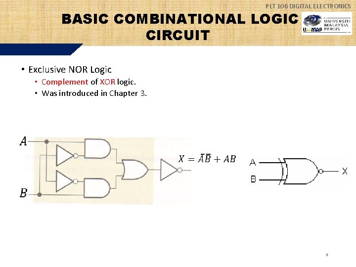
PLT 106 DIGITAL ELECTRONICS BASIC COMBINATIONAL LOGIC CIRCUIT • Exclusive NOR Logic • Complement of XOR logic. • Was introduced in Chapter 3. 6
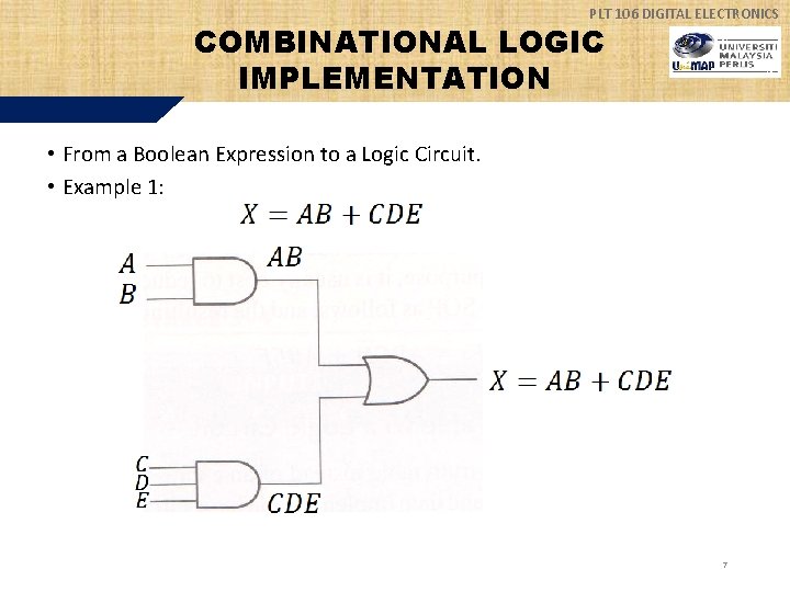
PLT 106 DIGITAL ELECTRONICS COMBINATIONAL LOGIC IMPLEMENTATION • From a Boolean Expression to a Logic Circuit. • Example 1: 7
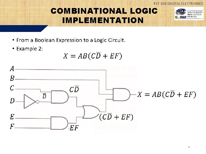
PLT 106 DIGITAL ELECTRONICS COMBINATIONAL LOGIC IMPLEMENTATION • From a Boolean Expression to a Logic Circuit. • Example 2: 8
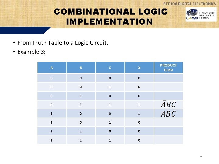
PLT 106 DIGITAL ELECTRONICS COMBINATIONAL LOGIC IMPLEMENTATION • From Truth Table to a Logic Circuit. • Example 3: A B C X 0 0 0 1 1 0 0 1 1 0 0 1 1 1 0 PRODUCT TERM 9
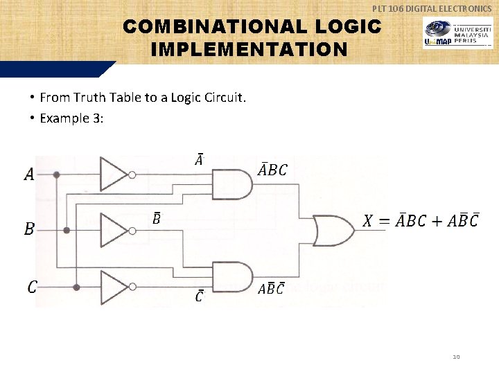
PLT 106 DIGITAL ELECTRONICS COMBINATIONAL LOGIC IMPLEMENTATION • From Truth Table to a Logic Circuit. • Example 3: 10
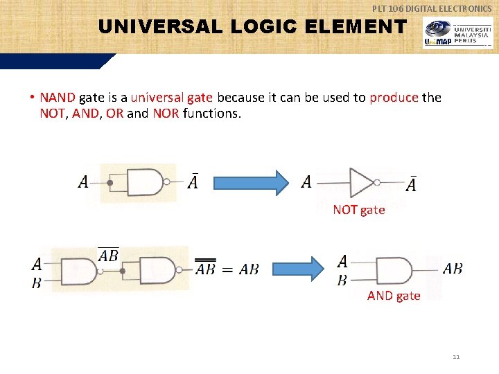
PLT 106 DIGITAL ELECTRONICS UNIVERSAL LOGIC ELEMENT • NAND gate is a universal gate because it can be used to produce the NOT, AND, OR and NOR functions. NOT gate AND gate 11
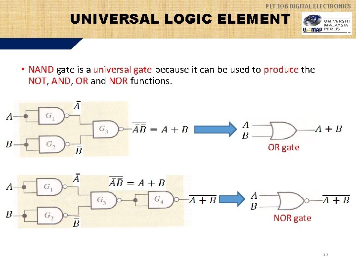
PLT 106 DIGITAL ELECTRONICS UNIVERSAL LOGIC ELEMENT • NAND gate is a universal gate because it can be used to produce the NOT, AND, OR and NOR functions. OR gate NOR gate 12
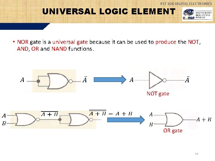
PLT 106 DIGITAL ELECTRONICS UNIVERSAL LOGIC ELEMENT • NOR gate is a universal gate because it can be used to produce the NOT, AND, OR and NAND functions. NOT gate OR gate 13
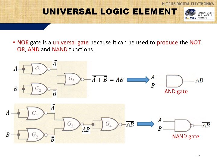
PLT 106 DIGITAL ELECTRONICS UNIVERSAL LOGIC ELEMENT • NOR gate is a universal gate because it can be used to produce the NOT, OR, AND and NAND functions. AND gate NAND gate 14
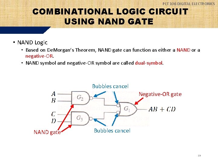
PLT 106 DIGITAL ELECTRONICS COMBINATIONAL LOGIC CIRCUIT USING NAND GATE • NAND Logic • Based on De. Morgan’s Theorem, NAND gate can function as either a NAND or a negative-OR. • NAND symbol and negative-OR symbol are called dual-symbol. Bubbles cancel Negative-OR gate NAND gate Bubbles cancel 15
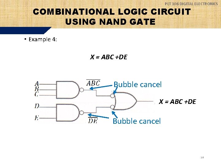
PLT 106 DIGITAL ELECTRONICS COMBINATIONAL LOGIC CIRCUIT USING NAND GATE • Example 4: X = ABC +DE Bubble cancel 16
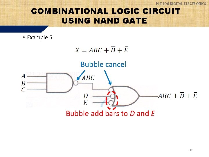
PLT 106 DIGITAL ELECTRONICS COMBINATIONAL LOGIC CIRCUIT USING NAND GATE • Example 5: Bubble cancel Bubble add bars to D and E 17
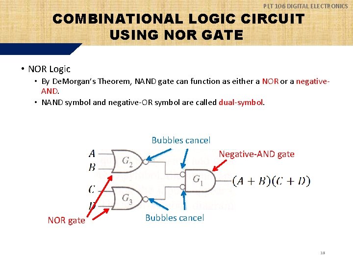
PLT 106 DIGITAL ELECTRONICS COMBINATIONAL LOGIC CIRCUIT USING NOR GATE • NOR Logic • By De. Morgan’s Theorem, NAND gate can function as either a NOR or a negative. AND. • NAND symbol and negative-OR symbol are called dual-symbol. Bubbles cancel Negative-AND gate NOR gate Bubbles cancel 18
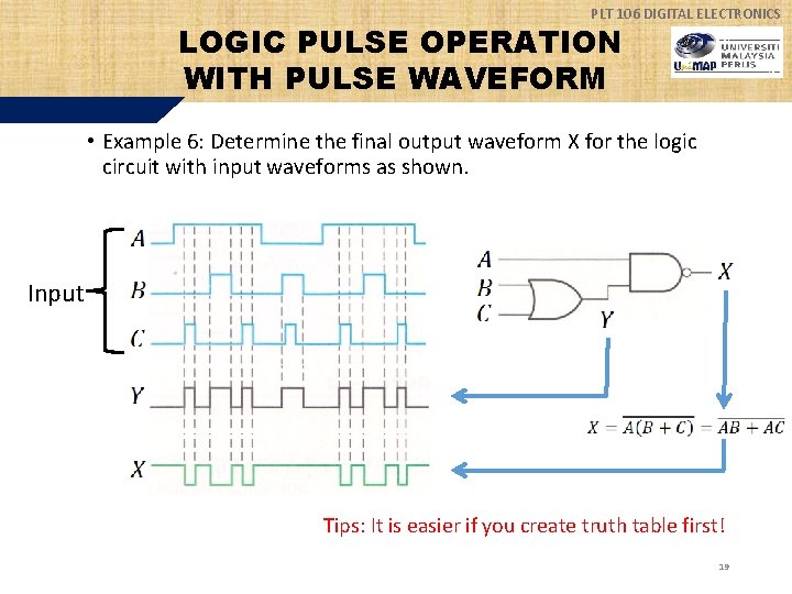
PLT 106 DIGITAL ELECTRONICS LOGIC PULSE OPERATION WITH PULSE WAVEFORM • Example 6: Determine the final output waveform X for the logic circuit with input waveforms as shown. Input Tips: It is easier if you create truth table first! 19
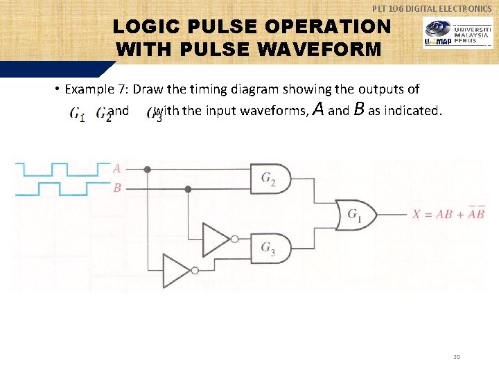
PLT 106 DIGITAL ELECTRONICS LOGIC PULSE OPERATION WITH PULSE WAVEFORM • Example 7: Draw the timing diagram showing the outputs of G 1, G 2 and G 3 with the input waveforms, A and B as indicated. 20
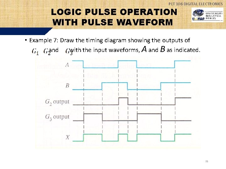
PLT 106 DIGITAL ELECTRONICS LOGIC PULSE OPERATION WITH PULSE WAVEFORM • Example 7: Draw the timing diagram showing the outputs of G 1, G 2 and G 3 with the input waveforms, A and B as indicated. 21
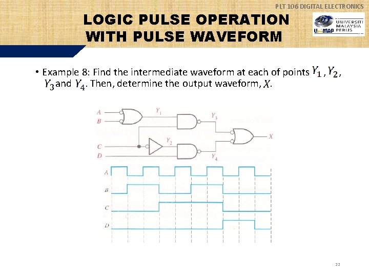
PLT 106 DIGITAL ELECTRONICS LOGIC PULSE OPERATION WITH PULSE WAVEFORM • Example 8: Find the intermediate waveform at each of points Y 1, Y 2, Y 3 and Y 4. Then, determine the output waveform, X. 22
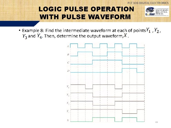
PLT 106 DIGITAL ELECTRONICS LOGIC PULSE OPERATION WITH PULSE WAVEFORM • Example 8: Find the intermediate waveform at each of points Y 1, Y 2, Y 3 and Y 4. Then, determine the output waveform, X. 23

THE END
- Slides: 24