PLT 106 DIGITAL ELECTRONICS CHAPTER 5 BASIC COMBINATIONAL
PLT 106: DIGITAL ELECTRONICS CHAPTER 5: BASIC COMBINATIONAL LOGIC CIRCUITS
Definition �Combination of basic gates to form circuits that can carry out a desired application. �In combinational logic, the output level is at all times dependent on the combination of input levels. �Combinational logic circuits contain no memory (no ability to store information). PLT 106 DIGITAL ELECTRONICS
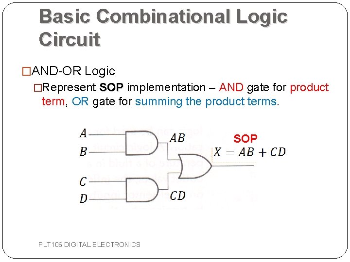
Basic Combinational Logic Circuit �AND-OR Logic �Represent SOP implementation – AND gate for product term, OR gate for summing the product terms. SOP PLT 106 DIGITAL ELECTRONICS
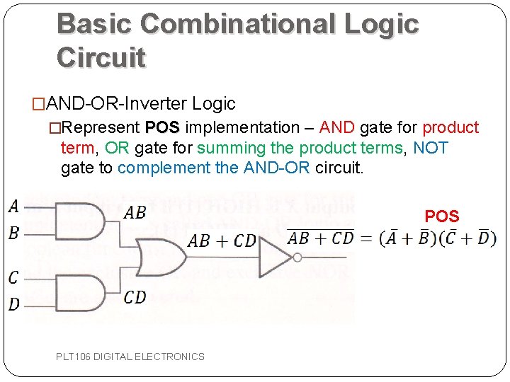
Basic Combinational Logic Circuit �AND-OR-Inverter Logic �Represent POS implementation – AND gate for product term, OR gate for summing the product terms, NOT gate to complement the AND-OR circuit. POS PLT 106 DIGITAL ELECTRONICS
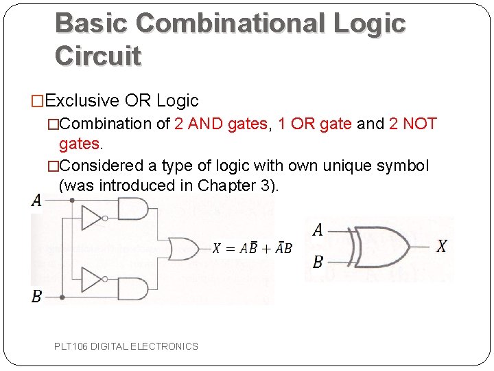
Basic Combinational Logic Circuit �Exclusive OR Logic �Combination of 2 AND gates, 1 OR gate and 2 NOT gates. �Considered a type of logic with own unique symbol (was introduced in Chapter 3). PLT 106 DIGITAL ELECTRONICS
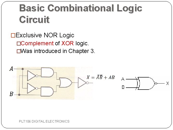
Basic Combinational Logic Circuit �Exclusive NOR Logic �Complement of XOR logic. �Was introduced in Chapter 3. PLT 106 DIGITAL ELECTRONICS
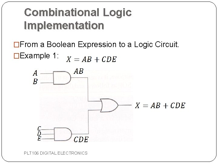
Combinational Logic Implementation �From a Boolean Expression to a Logic Circuit. �Example 1: PLT 106 DIGITAL ELECTRONICS
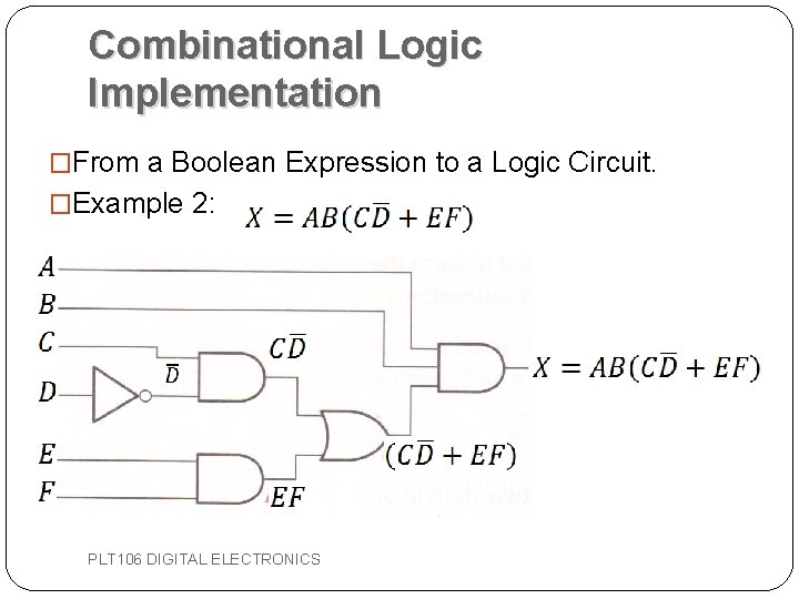
Combinational Logic Implementation �From a Boolean Expression to a Logic Circuit. �Example 2: PLT 106 DIGITAL ELECTRONICS
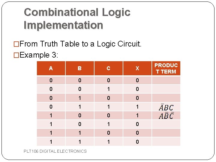
Combinational Logic Implementation �From Truth Table to a Logic Circuit. �Example 3: A B C X 0 0 0 1 1 0 0 1 1 0 0 1 1 1 0 PLT 106 DIGITAL ELECTRONICS PRODUC T TERM
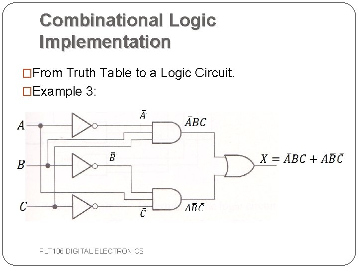
Combinational Logic Implementation �From Truth Table to a Logic Circuit. �Example 3: PLT 106 DIGITAL ELECTRONICS
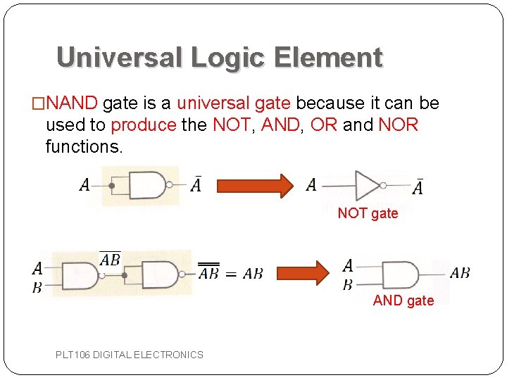
Universal Logic Element �NAND gate is a universal gate because it can be used to produce the NOT, AND, OR and NOR functions. NOT gate AND gate PLT 106 DIGITAL ELECTRONICS
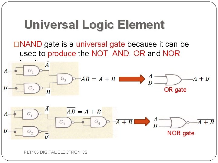
Universal Logic Element �NAND gate is a universal gate because it can be used to produce the NOT, AND, OR and NOR functions. OR gate NOR gate PLT 106 DIGITAL ELECTRONICS
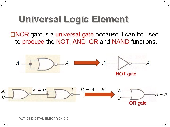
Universal Logic Element �NOR gate is a universal gate because it can be used to produce the NOT, AND, OR and NAND functions. NOT gate OR gate PLT 106 DIGITAL ELECTRONICS
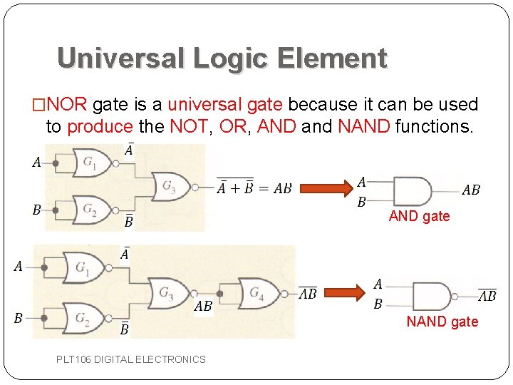
Universal Logic Element �NOR gate is a universal gate because it can be used to produce the NOT, OR, AND and NAND functions. AND gate NAND gate PLT 106 DIGITAL ELECTRONICS
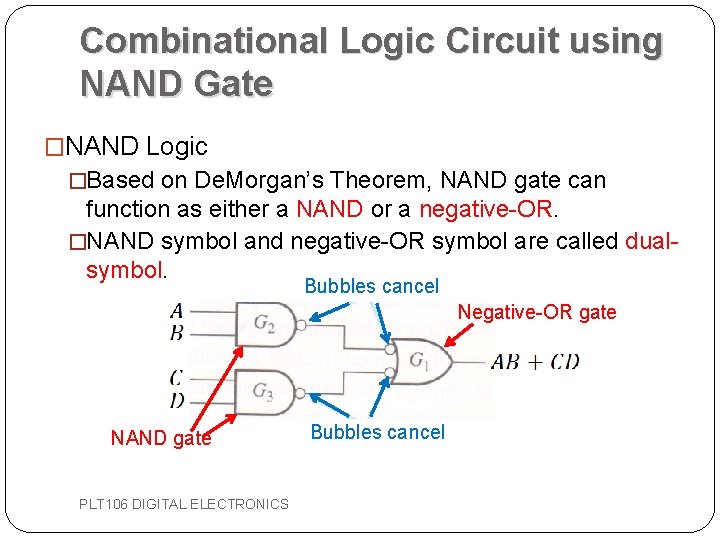
Combinational Logic Circuit using NAND Gate �NAND Logic �Based on De. Morgan’s Theorem, NAND gate can function as either a NAND or a negative-OR. �NAND symbol and negative-OR symbol are called dualsymbol. Bubbles cancel Negative-OR gate NAND gate PLT 106 DIGITAL ELECTRONICS Bubbles cancel
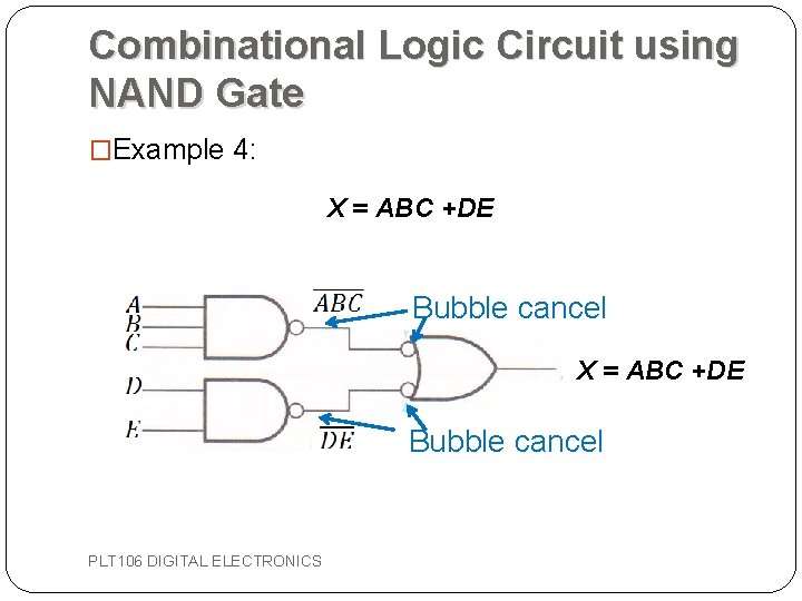
Combinational Logic Circuit using NAND Gate �Example 4: X = ABC +DE Bubble cancel PLT 106 DIGITAL ELECTRONICS
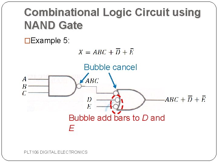
Combinational Logic Circuit using NAND Gate �Example 5: Bubble cancel Bubble add bars to D and E PLT 106 DIGITAL ELECTRONICS
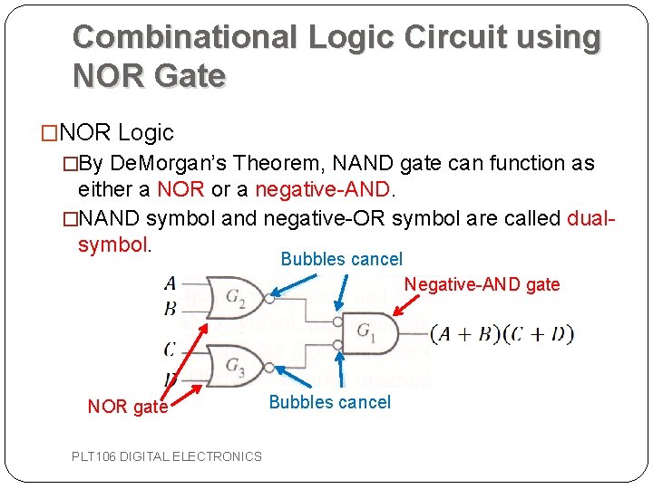
Combinational Logic Circuit using NOR Gate �NOR Logic �By De. Morgan’s Theorem, NAND gate can function as either a NOR or a negative-AND. �NAND symbol and negative-OR symbol are called dualsymbol. Bubbles cancel Negative-AND gate NOR gate PLT 106 DIGITAL ELECTRONICS Bubbles cancel
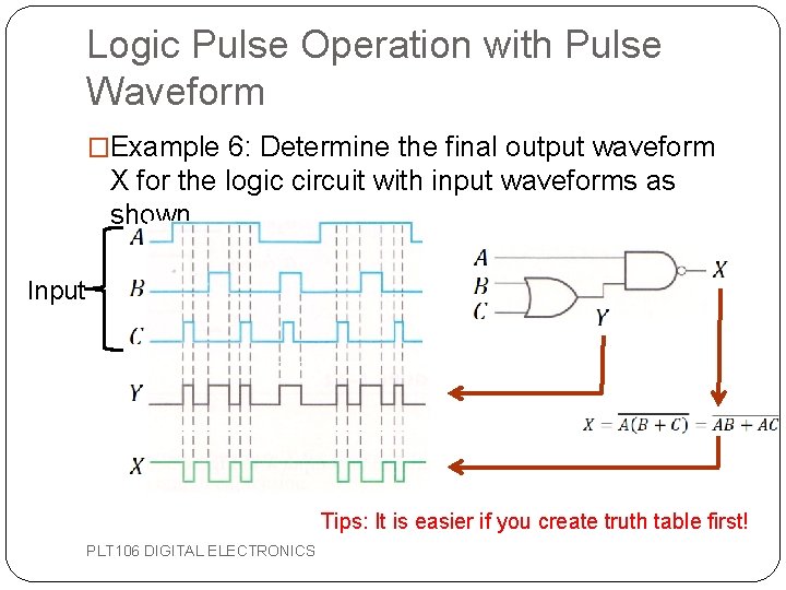
Logic Pulse Operation with Pulse Waveform �Example 6: Determine the final output waveform X for the logic circuit with input waveforms as shown. Input Tips: It is easier if you create truth table first! PLT 106 DIGITAL ELECTRONICS
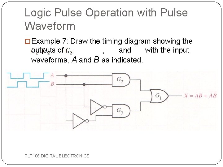
Logic Pulse Operation with Pulse Waveform � Example 7: Draw the timing diagram showing the outputs of G 1, G 2 and G 3 with the input waveforms, A and B as indicated. PLT 106 DIGITAL ELECTRONICS
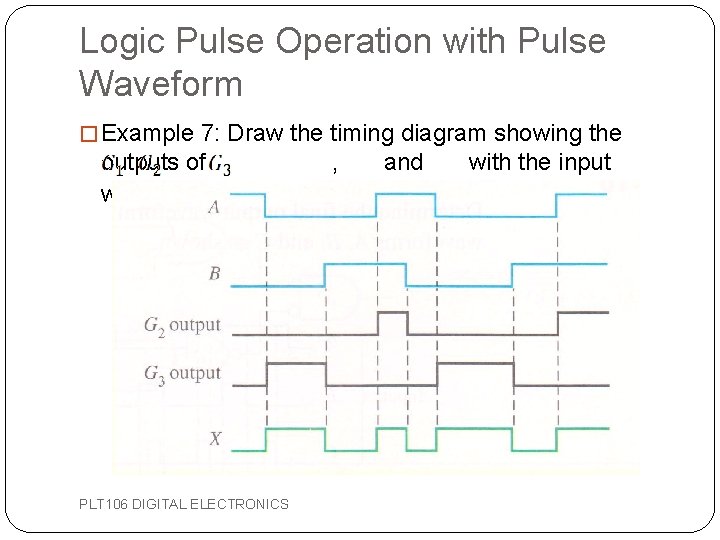
Logic Pulse Operation with Pulse Waveform � Example 7: Draw the timing diagram showing the outputs of G 1, G 2 and G 3 with the input waveforms, A and B as indicated. PLT 106 DIGITAL ELECTRONICS
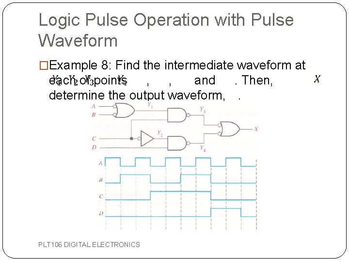
Logic Pulse Operation with Pulse Waveform �Example 8: Find the intermediate waveform at each of points Y 1, Y 2, Y 3 and Y 4. Then, determine the output waveform, X. PLT 106 DIGITAL ELECTRONICS
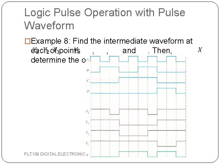
Logic Pulse Operation with Pulse Waveform �Example 8: Find the intermediate waveform at each of points Y 1, Y 2, Y 3 and Y 4. Then, determine the output waveform, X. PLT 106 DIGITAL ELECTRONICS

THE END
- Slides: 24