Plasma Enhanced Chemical Vapor Deposition cntd Outline Plasma

- Slides: 39


Plasma Enhanced Chemical Vapor Deposition (cntd. )

Outline • Plasma Deposition Introduction • Deposition Coverage • The Six Basic Steps of Chemical Vapor Deposition • Film Growth • Issues Concerning PECVD Deposition • Types of PECVD Deposition

Plasma Deposition Introduction • Plasma processing can be used to: – Deposit material (PECVD) – Remove material (etching, ashing, etc) – Modify the surface through bombardment – Chemically modify the surface • These scenarios are complex chemical processes • Generally these consequences occur during any planned process, but the recipes are designed to have one result dominate

Plasma Enhanced Chemical Vapor Deposition • The deposition of films using plasma offers the unique combination of low temperature and good film composition and coverage • Some PECVD systems have the ability to etch and clean the substrate prior to deposition, reducing contamination

Plasma Deposition Introduction • RF power is used to break up gas molecules in a vacuum • Molecular fragments (radicals) readily bond to other atoms to form a film at the substrate’s surface • Gaseous by-products are removed by the vacuum pumping system • The substrate may be heated to increase surface reactions and drive out contaminants

Outline • Plasma Deposition Introduction • Deposition Coverage • The Six Basic Steps of Chemical Vapor Deposition • Film Growth • Issues Concerning PECVD Deposition • Types of PECVD Deposition

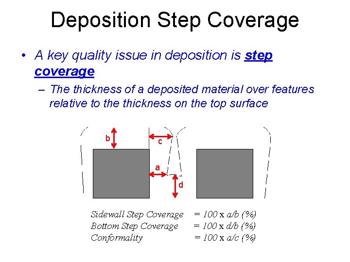
Deposition Step Coverage • A key quality issue in deposition is step coverage – The thickness of a deposited material over features relative to the thickness on the top surface b c a d Sidewall Step Coverage = 100 x a/b (%) Bottom Step Coverage = 100 x d/b (%) Conformality = 100 x a/c (%)

Deposition Uniformity • Insuring uniform coverage – The substrate chuck is heated to control the morphology of the deposition – Plasma ion bombardment is also used to increase the mobility of adatoms

Outline • Plasma Deposition Introduction • Deposition Coverage • The Six Basic Steps of Chemical Vapor Deposition • Film Growth • Issues Concerning PECVD Deposition • Types of PECVD Deposition

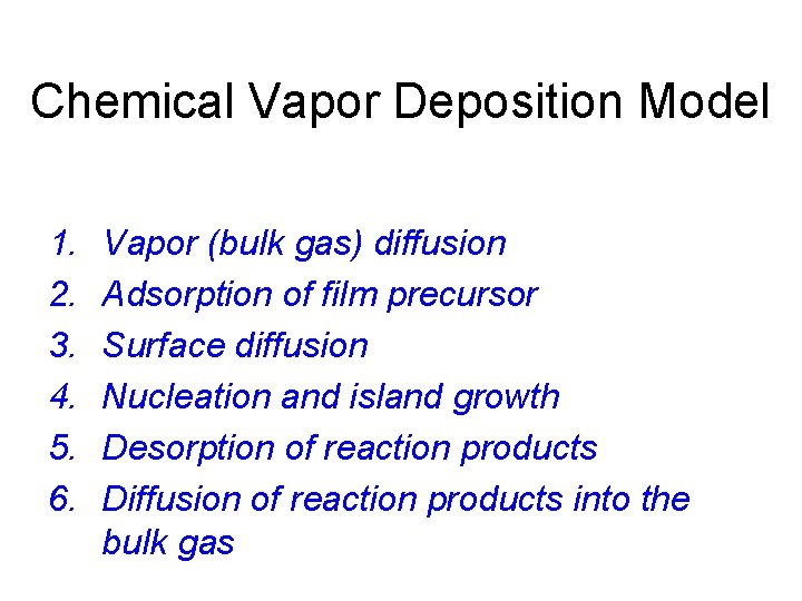
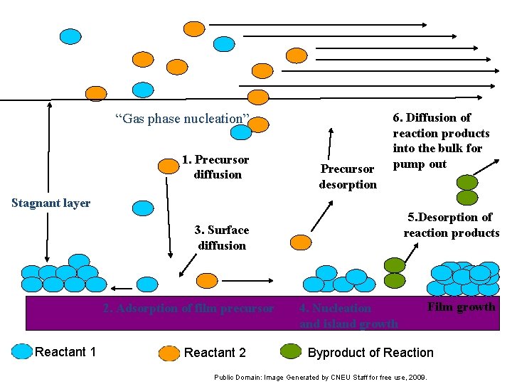
Chemical Vapor Deposition Model 1. 2. 3. 4. 5. 6. Vapor (bulk gas) diffusion Adsorption of film precursor Surface diffusion Nucleation and island growth Desorption of reaction products Diffusion of reaction products into the bulk gas

“Gas phase nucleation” 1. Precursor diffusion Precursor desorption 6. Diffusion of reaction products into the bulk for pump out Stagnant layer 5. Desorption of reaction products 3. Surface diffusion 2. Adsorption of film precursor Reactant 1 Reactant 2 4. Nucleation and island growth Film growth Byproduct of Reaction Public Domain: Image Generated by CNEU Staff for free use, 2009.

Outline • Plasma Deposition Introduction • Deposition Coverage • The Six Basic Steps of Chemical Vapor Deposition • Film Growth • Issues Concerning PECVD Deposition • Types of PECVD Deposition

Forming a Film • Given enough time and surface mobility, a deposited film grows in three stages – Nucleation – Island growth – Coalescence

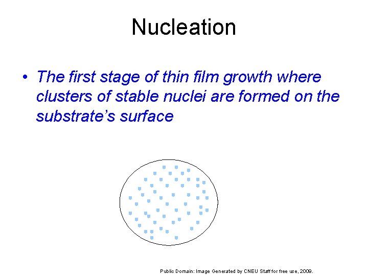
Nucleation • The first stage of thin film growth where clusters of stable nuclei are formed on the substrate’s surface Public Domain: Image Generated by CNEU Staff for free use, 2009.

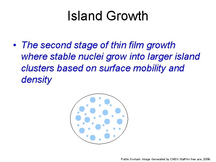
Island Growth • The second stage of thin film growth where stable nuclei grow into larger island clusters based on surface mobility and density Public Domain: Image Generated by CNEU Staff for free use, 2009.

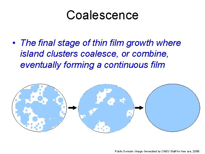
Coalescence • The final stage of thin film growth where island clusters coalesce, or combine, eventually forming a continuous film Public Domain: Image Generated by CNEU Staff for free use, 2009.

Outline • Plasma Deposition Introduction • Deposition Coverage • The Six Basic Steps of Chemical Vapor Deposition • Film Growth • Issues Concerning PECVD Deposition • Types of PECVD Deposition

Quality Issues in CVD • • Film Density Film Stress Included Contaminants Surface Damage

Advantages of PECVD • Lower processing temperature (~150 to 450 o. C), gives a wide range of applications • Excellent gap-fill for high aspect ratio gaps (low density plasma) • Good film adhesion to the substrate • High deposition rates • Can have high film density due to few pinholes and voids

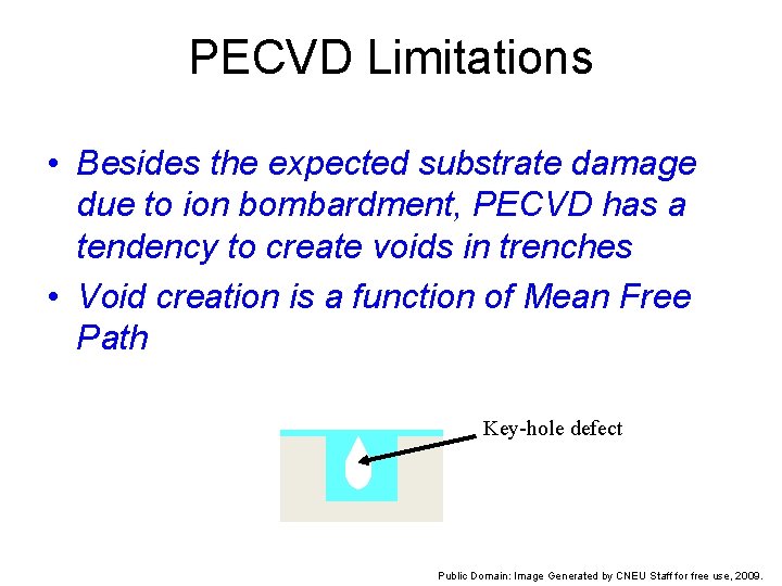
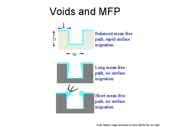
PECVD Limitations • Besides the expected substrate damage due to ion bombardment, PECVD has a tendency to create voids in trenches • Void creation is a function of Mean Free Path Key-hole defect Public Domain: Image Generated by CNEU Staff for free use, 2009.

Voids and MFP Balanced mean free path, rapid surface migration D W Long mean free path, no surface migration Short mean free path, no surface migration Public Domain: Image Generated by CNEU Staff for free use, 2009.

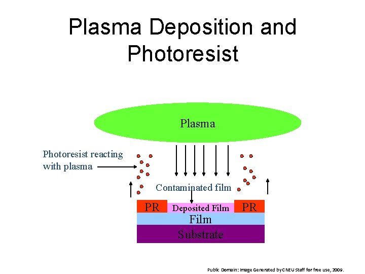
Plasma Deposition and Photoresist • Unlike etching, photoresist is undesirable for plasma depositions – Besides thermal flow due to a heated substrate chuck, plasma will react with the photoresist resulting in a volatile product that contaminates the film

Plasma Deposition and Photoresist Plasma Photoresist reacting with plasma Contaminated film PR Deposited Film Substrate PR Public Domain: Image Generated by CNEU Staff for free use, 2009.

Outline • Plasma Deposition Introduction • Deposition Coverage • The Six Basic Steps of Chemical Vapor Deposition • Film Growth • Issues Concerning PECVD Deposition • Types of PECVD Deposition

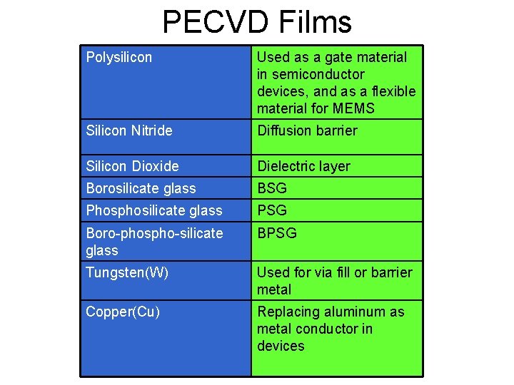
PECVD Films Polysilicon Used as a gate material in semiconductor devices, and as a flexible material for MEMS Silicon Nitride Diffusion barrier Silicon Dioxide Dielectric layer Borosilicate glass BSG Phosphosilicate glass PSG Boro-phospho-silicate glass BPSG Tungsten(W) Used for via fill or barrier metal Copper(Cu) Replacing aluminum as metal conductor in devices

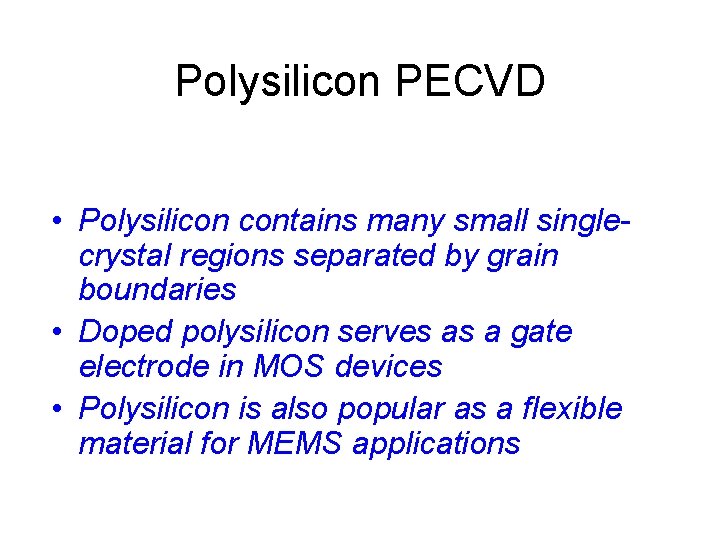
Polysilicon PECVD • Polysilicon contains many small singlecrystal regions separated by grain boundaries • Doped polysilicon serves as a gate electrode in MOS devices • Polysilicon is also popular as a flexible material for MEMS applications

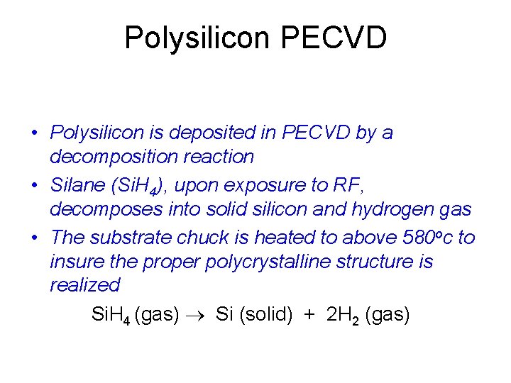
Polysilicon PECVD • Polysilicon is deposited in PECVD by a decomposition reaction • Silane (Si. H 4), upon exposure to RF, decomposes into solid silicon and hydrogen gas • The substrate chuck is heated to above 580 oc to insure the proper polycrystalline structure is realized Si. H 4 (gas) Si (solid) + 2 H 2 (gas)

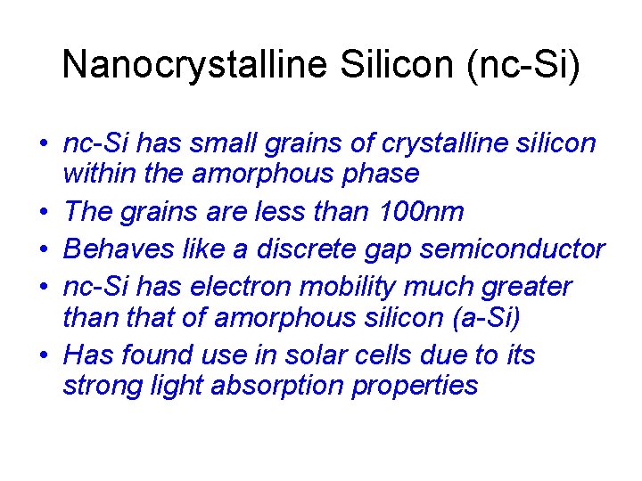
Nanocrystalline Silicon (nc-Si) • nc-Si has small grains of crystalline silicon within the amorphous phase • The grains are less than 100 nm • Behaves like a discrete gap semiconductor • nc-Si has electron mobility much greater than that of amorphous silicon (a-Si) • Has found use in solar cells due to its strong light absorption properties

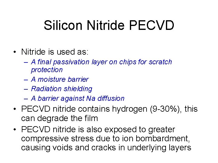
Silicon Nitride PECVD • Nitride is used as: – A final passivation layer on chips for scratch protection – A moisture barrier – Radiation shielding – A barrier against Na diffusion • PECVD nitride contains hydrogen (9 -30%), this can degrade the film • PECVD nitride is also exposed to greater compressive stress due to ion bombardment, causing voids and cracks in underlying layers

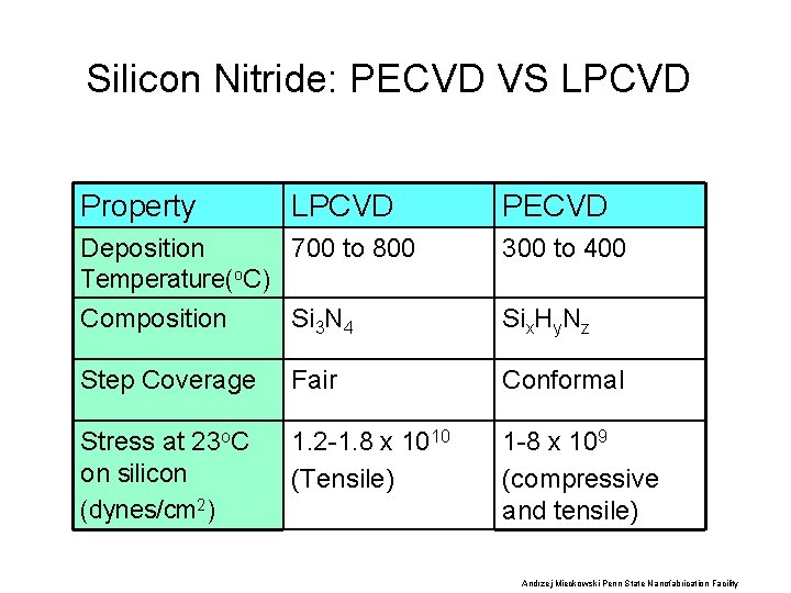
Silicon Nitride: PECVD VS LPCVD Property LPCVD PECVD Deposition 700 to 800 Temperature(o. C) 300 to 400 Composition Si 3 N 4 Six. Hy. Nz Step Coverage Fair Conformal Stress at 23 o. C on silicon (dynes/cm 2) 1. 2 -1. 8 x 10¹⁰ (Tensile) 1 -8 x 10⁹ (compressive and tensile) Andrzej Mieckowski Penn State Nanofabrication Facility

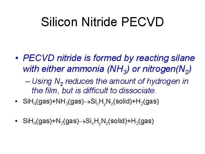
Silicon Nitride PECVD • PECVD nitride is formed by reacting silane with either ammonia (NH 3) or nitrogen(N 2) – Using N 2 reduces the amount of hydrogen in the film, but is difficult to dissociate. • Si. H 4(gas)+NH 3(gas) Six. Hy. Nz(solid)+H 2(gas) • Si. H 4(gas)+N 2(gas) Six. Hy. Nz(solid)+H 2(gas)

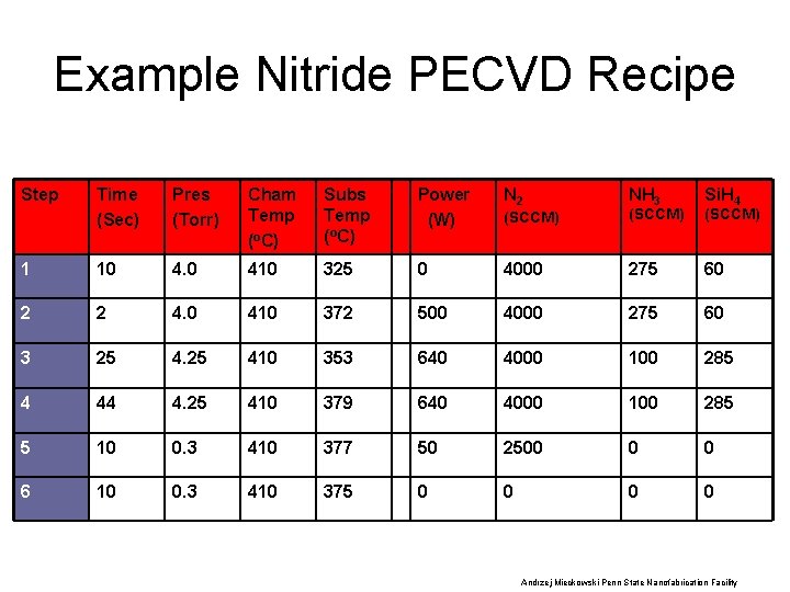
Example Nitride PECVD Recipe Step Time (Sec) Pres (Torr) Cham Temp (o. C) Subs Temp (o. C) Power (W) N 2 NH 3 (SCCM) Si. H 4 1 10 4. 0 410 325 0 4000 275 60 2 2 4. 0 410 372 500 4000 275 60 3 25 410 353 640 4000 100 285 4 44 4. 25 410 379 640 4000 100 285 5 10 0. 3 410 377 50 2500 0 0 6 10 0. 3 410 375 0 0 (SCCM) Andrzej Mieckowski Penn State Nanofabrication Facility

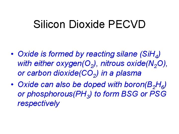
Silicon Dioxide PECVD • Oxide is formed by reacting silane (Si. H 4) with either oxygen(O 2), nitrous oxide(N 2 O), or carbon dioxide(CO 2) in a plasma • Oxide can also be doped with boron(B 2 H 6) or phosphorous(PH 3) to form BSG or PSG respectively

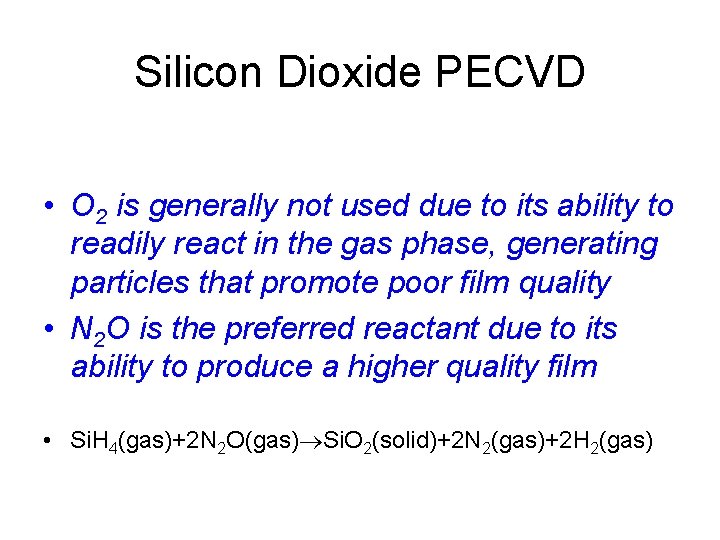
Silicon Dioxide PECVD • O 2 is generally not used due to its ability to readily react in the gas phase, generating particles that promote poor film quality • N 2 O is the preferred reactant due to its ability to produce a higher quality film • Si. H 4(gas)+2 N 2 O(gas) Si. O 2(solid)+2 N 2(gas)+2 H 2(gas)

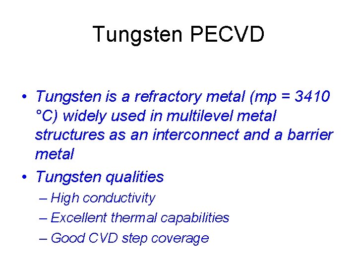
Tungsten PECVD • Tungsten is a refractory metal (mp = 3410 °C) widely used in multilevel metal structures as an interconnect and a barrier metal • Tungsten qualities – High conductivity – Excellent thermal capabilities – Good CVD step coverage

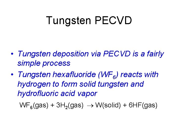
Tungsten PECVD • Tungsten deposition via PECVD is a fairly simple process • Tungsten hexafluoride (WF 6) reacts with hydrogen to form solid tungsten and hydrofluoric acid vapor WF 6(gas) + 3 H 2(gas) W(solid) + 6 HF(gas)

Copper PECVD • Copper is replacing aluminum as the metal conductor of choice in high speed devices • Copper qualities – Excellent conductivity – Low production cost – Good step coverage

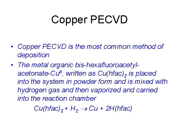
Copper PECVD • Copper PECVD is the most common method of deposition • The metal organic bis-hexafluoroacetylacetonate-Cu. II, written as Cu(hfac)2 is placed into the system in powder form and is mixed with hydrogen gas and then vaporized and carried into the reaction chamber Cu(hfac)2 + H 2 Cu + 2 H(hfac)