Planar nMOSFET crosssection and layout The designer introduces




- Slides: 48

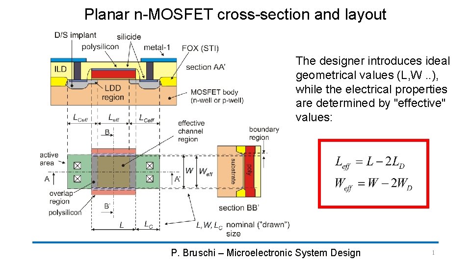
Planar n-MOSFET cross-section and layout The designer introduces ideal geometrical values (L, W. . ), while the electrical properties are determined by "effective" values: P. Bruschi – Microelectronic System Design 1

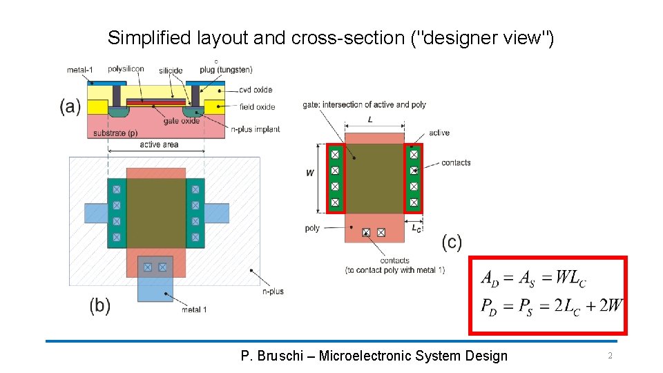
Simplified layout and cross-section ("designer view") P. Bruschi – Microelectronic System Design 2

MOSFET models • Models for accurate electrical simulations (BSIM models, EKV …) • Models for "hand calculations": square law (strong inversion) exponential laws (weak inversion) • It is of primary importance to be able to perform first order device sizing and first order performance estimation. • Only very simple and intuitive model enable the designer to create cells that need only a final refinement and verification in the simulation phase • The simulator is useless if we do not know how to produce a circuit on scrap-paper. The simulator obeys to the law: garbage in – garbage out P. Bruschi – Microelectronic System Design 3

MOSFET models: The n-MOSFET • From this point on, we will consider the behavior of the n-MOSFET, unless otherwise specified. In the end, we will suggest a simple way to transfer all the considerations made for the n-MOSFET to the p-MOSFET • In integrated circuits, the MOSFET is a four terminal devices: Drain, Source, Gate and Body. In discrete MOSFETs, the body is generally connected to the source internally. D G B S P. Bruschi – Microelectronic System Design 4

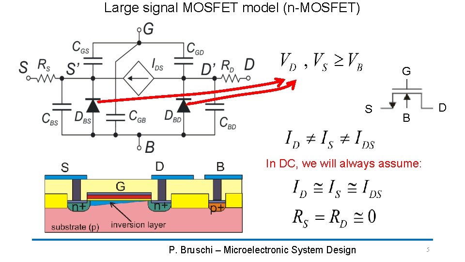
Large signal MOSFET model (n-MOSFET) G S D B In DC, we will always assume: P. Bruschi – Microelectronic System Design 5

Source and Drain Symmetry (1) • The planar MOSFET is symmetric so that drain and source can be swapped with no consequences in the electrical characteristics. • Equations that use the source as a reference terminal for all relevant voltages can be applied only after finding which terminal is actually playing the role of the source. • In an n-MOSFET, the actual source is the terminal that have the lower voltage; the other one of the two, is the actual drain • In a p-MOSFET, the actual source is the terminal that have the higher voltage; the other one of the two, is the actual drain P. Bruschi – Microelectronic System Design 6

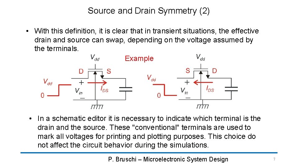
Source and Drain Symmetry (2) • With this definition, it is clear that in transient situations, the effective drain and source can swap, depending on the voltage assumed by the terminals. Example • In a schematic editor it is necessary to indicate which terminal is the drain and the source. These "conventional" terminals are used to mark all voltages for printing and plotting purposes. This choice do not affect the circuit behavior during the simulations. P. Bruschi – Microelectronic System Design 7

Source and Drain Symmetry (3) • If the circuit has a clear static operating point (like most analog circuits), it is convenient to mark as source the terminal that in the operating point is actually working as the source. This will facilitate reading device voltages produced as textual or graphical outputs by the simulator. • Models like the EKV use the body as the reference for all voltages. In this way drain and sources are perfectly symmetrical also in the equations and there is no need to decide which one is actually working as the source. • Maintaining the distinction between source and drain is more intuitive and most models oriented to hand calculations are actually based on this choice. P. Bruschi – Microelectronic System Design 8

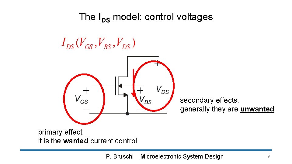
The IDS model: control voltages secondary effects: generally they are unwanted primary effect it is the wanted current control P. Bruschi – Microelectronic System Design 9

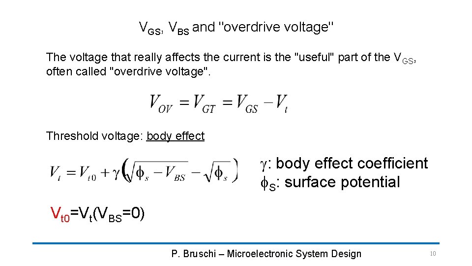
VGS, VBS and "overdrive voltage" The voltage that really affects the current is the "useful" part of the V GS, often called "overdrive voltage". Threshold voltage: body effect g: body effect coefficient f. S: surface potential Vt 0=Vt(VBS=0) P. Bruschi – Microelectronic System Design 10

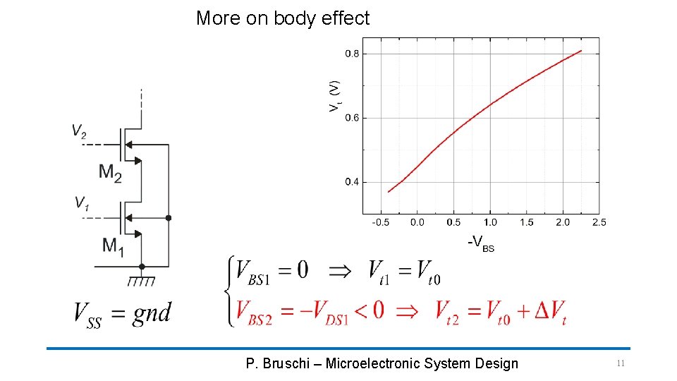
More on body effect P. Bruschi – Microelectronic System Design 11

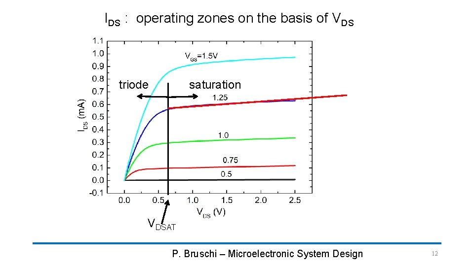
IDS : operating zones on the basis of VDS triode saturation VDSAT P. Bruschi – Microelectronic System Design 12

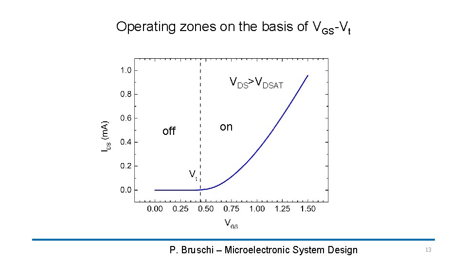
Operating zones on the basis of VGS-Vt VDS>VDSAT off on P. Bruschi – Microelectronic System Design 13

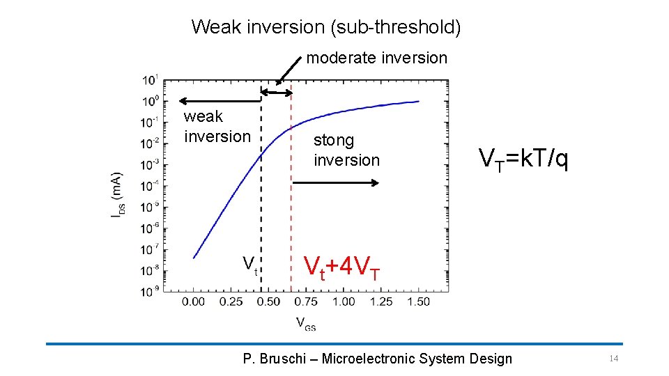
Weak inversion (sub-threshold) moderate inversion weak inversion stong inversion VT=k. T/q Vt+4 VT P. Bruschi – Microelectronic System Design 14

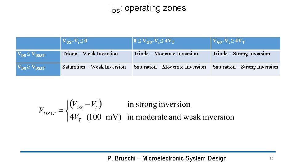
IDS: operating zones VGS -Vt ≤ 0 0 ≤ VGS -Vt ≤ 4 VT VGS -Vt ≥ 4 VT VDS ≤ VDSAT Triode – Weak Inversion Triode – Moderate Inversion Triode – Strong Inversion VDS ≥ VDSAT Saturation – Weak Inversion Saturation – Moderate Inversion Saturation – Strong Inversion P. Bruschi – Microelectronic System Design 15

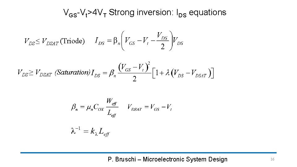
VGS-Vt>4 VT Strong inversion: IDS equations VDS ≤ VDSAT (Triode) VDS ≥ VDSAT (Saturation) P. Bruschi – Microelectronic System Design 16

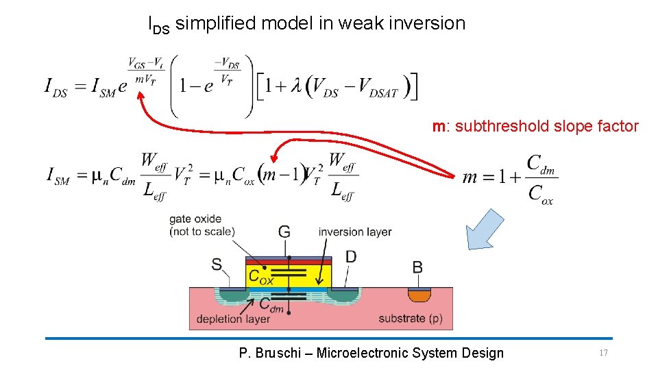
IDS simplified model in weak inversion m: subthreshold slope factor P. Bruschi – Microelectronic System Design 17

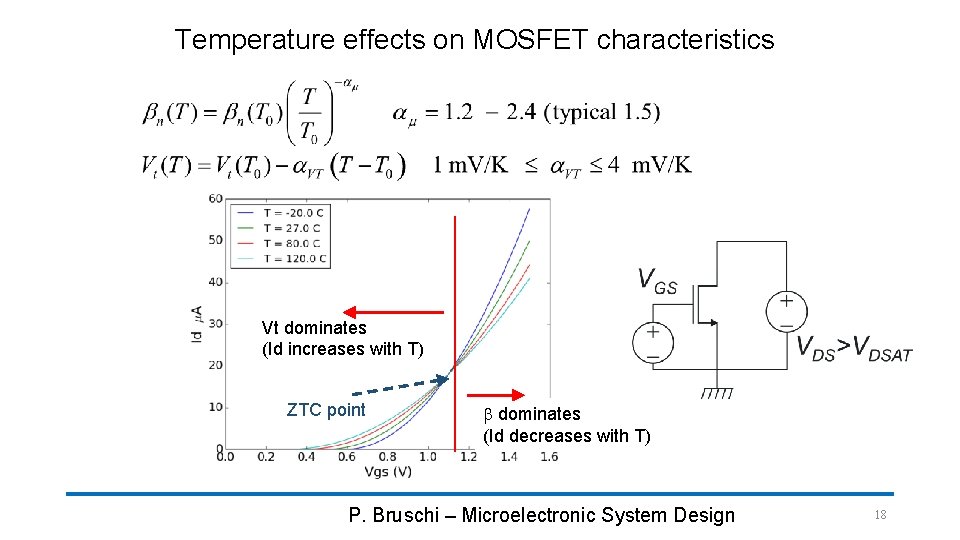
Temperature effects on MOSFET characteristics Vt dominates (Id increases with T) ZTC point b dominates (Id decreases with T) P. Bruschi – Microelectronic System Design 18

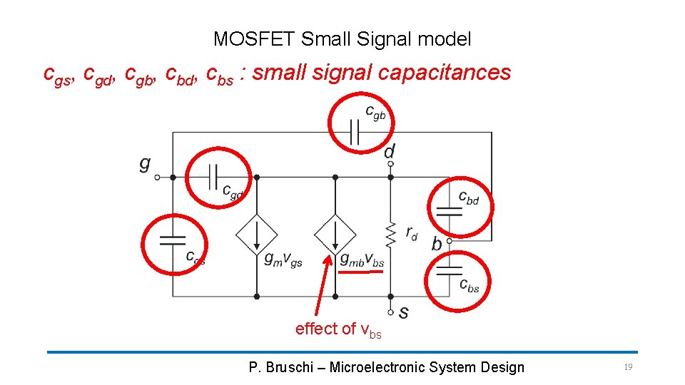
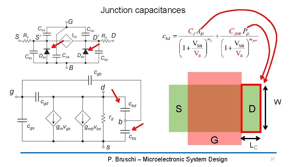
MOSFET Small Signal model cgs, cgd, cgb, cbd, cbs : small signal capacitances effect of vbs P. Bruschi – Microelectronic System Design 19

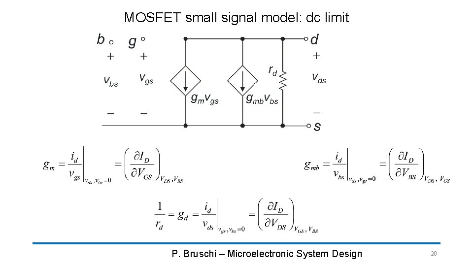
MOSFET small signal model: dc limit P. Bruschi – Microelectronic System Design 20

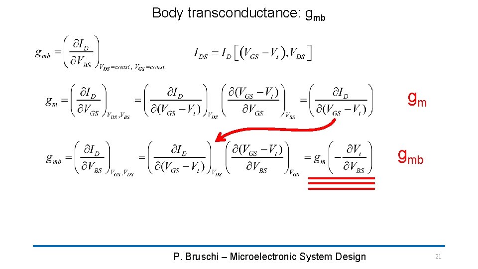
Body transconductance: gmb gm gmb P. Bruschi – Microelectronic System Design 21

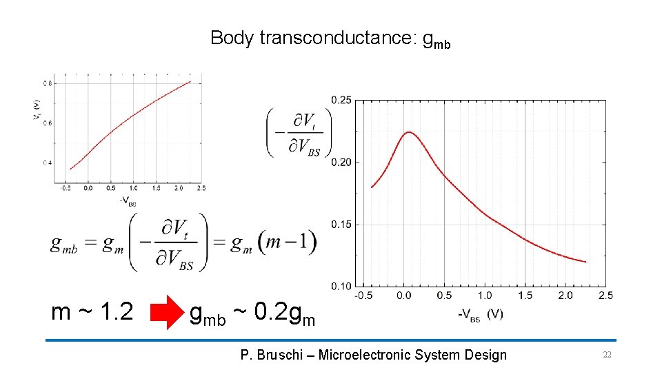
Body transconductance: gmb m ~ 1. 2 gmb ~ 0. 2 gm P. Bruschi – Microelectronic System Design 22

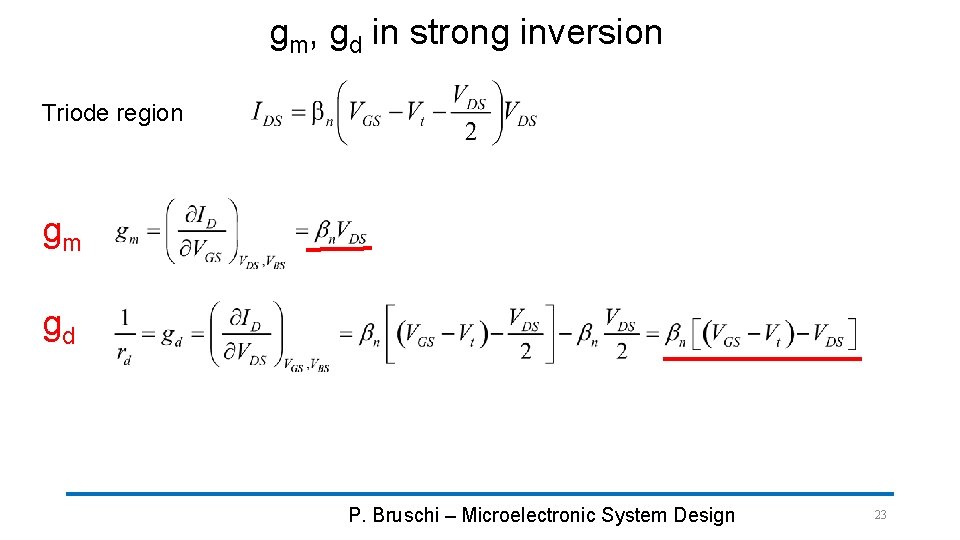
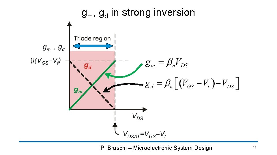
gm, gd in strong inversion Triode region gm gd P. Bruschi – Microelectronic System Design 23

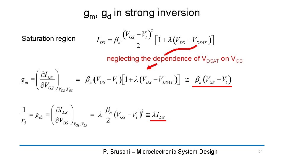
gm, gd in strong inversion Saturation region neglecting the dependence of VDSAT on VGS P. Bruschi – Microelectronic System Design 24

gm, gd in strong inversion P. Bruschi – Microelectronic System Design 25

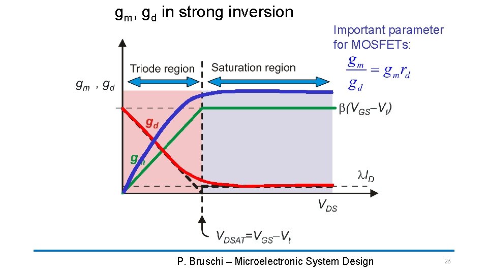
gm, gd in strong inversion Important parameter for MOSFETs: P. Bruschi – Microelectronic System Design 26

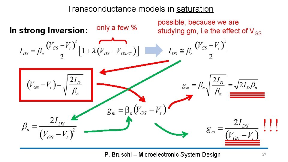
Transconductance models in saturation In strong Inversion: only a few % possible, because we are studying gm, i. e the effect of VGS !!! P. Bruschi – Microelectronic System Design 27

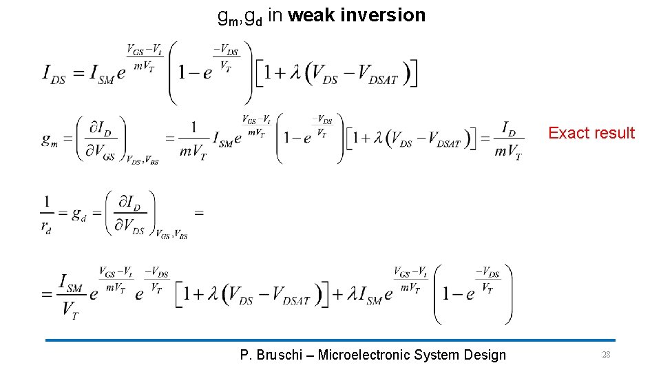
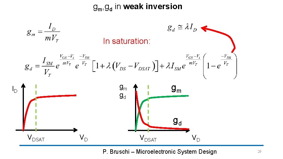
gm, gd in weak inversion Exact result P. Bruschi – Microelectronic System Design 28

gm, gd in weak inversion In saturation: gm gm gd ID gd VDSAT VD P. Bruschi – Microelectronic System Design 29

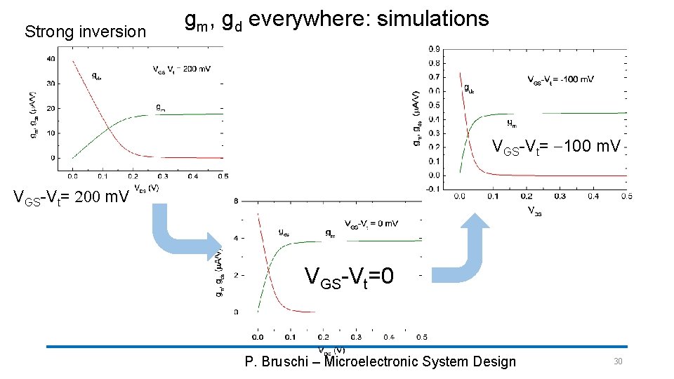
Strong inversion gm, gd everywhere: simulations VGS-Vt= -100 m. V VGS-Vt= 200 m. V VGS-Vt=0 P. Bruschi – Microelectronic System Design 30

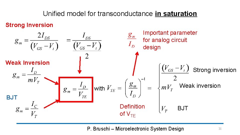
Unified model for transconductance in saturation Strong Inversion Important parameter for analog circuit design Weak Inversion Strong inversion Weak inversion with BJT Definition of VTE BJT P. Bruschi – Microelectronic System Design 31

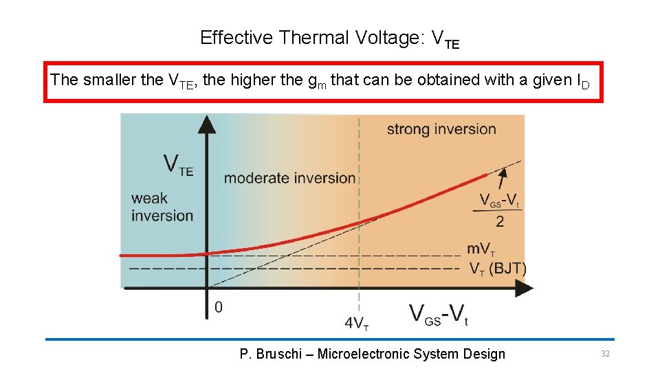
Effective Thermal Voltage: VTE The smaller the VTE, the higher the gm that can be obtained with a given ID P. Bruschi – Microelectronic System Design 32

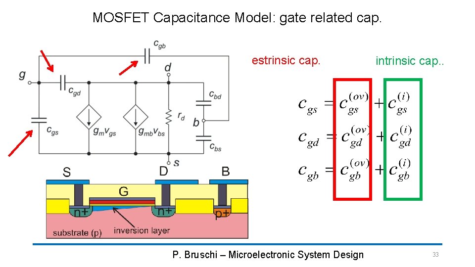
MOSFET Capacitance Model: gate related cap. estrinsic cap. P. Bruschi – Microelectronic System Design intrinsic cap. . 33

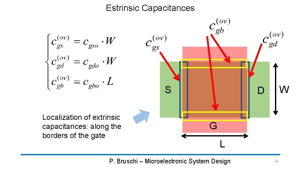
Estrinsic Capacitances S Localization of extrinsic capacitances: along the borders of the gate W D G L P. Bruschi – Microelectronic System Design 34

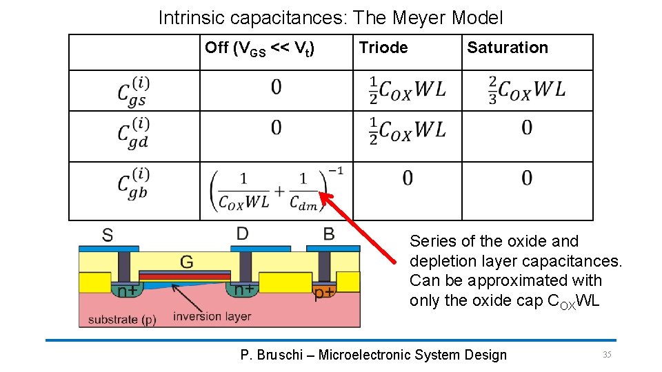
Intrinsic capacitances: The Meyer Model Off (VGS << Vt) Triode Saturation Series of the oxide and depletion layer capacitances. Can be approximated with only the oxide cap COXWL P. Bruschi – Microelectronic System Design 35

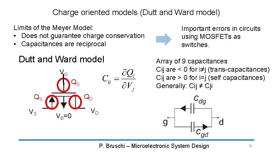
Charge oriented models (Dutt and Ward model) Limits of the Meyer Model: • Does not guarantee charge conservation • Capacitances are reciprocal Dutt and Ward model VG QG Array of 9 capacitances Cij are < 0 for i≠j (trans-capacitances) Cij are > 0 for i=j (self capacitances) Generally: Cij ≠ Cji QD QS VS Important errors in circuits using MOSFETs as switches. VB=0 VD P. Bruschi – Microelectronic System Design 36

Junction capacitances S D G P. Bruschi – Microelectronic System Design W LC 37

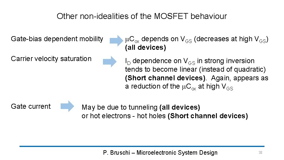
Other non-idealities of the MOSFET behaviour Gate-bias dependent mobility m. Cox depends on VGS (decreases at high VGS) (all devices) Carrier velocity saturation ID dependence on VGS in strong inversion tends to become linear (instead of quadratic) (Short channel devices). Again, appears as a reduction of the m. Cox at high VGS Gate current May be due to tunneling (all devices) or hot electrons - hot holes (Short channel devices) P. Bruschi – Microelectronic System Design 38

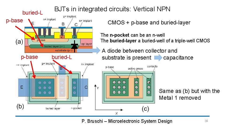
buried-L p-base BJTs in integrated circuits: Vertical NPN CMOS + p-base and buried-layer The n-pocket can be an n-well The buried-layer a buried-well of a triple-well CMOS p-base buried-L A diode between collector and substrate is present capacitance Same as (b) but with the Metal 1 removed P. Bruschi – Microelectronic System Design 39

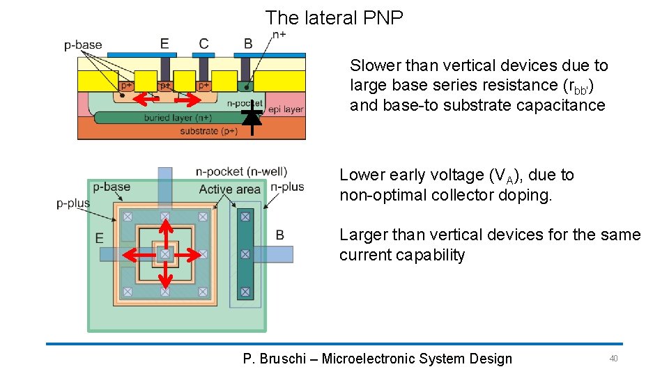
The lateral PNP Slower than vertical devices due to large base series resistance (rbb') and base-to substrate capacitance Lower early voltage (VA), due to non-optimal collector doping. Larger than vertical devices for the same current capability P. Bruschi – Microelectronic System Design 40

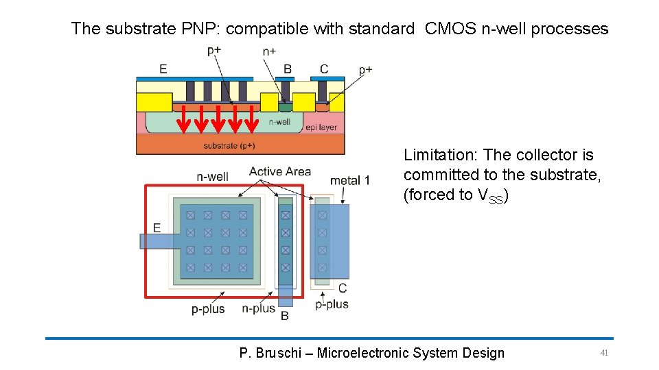
The substrate PNP: compatible with standard CMOS n-well processes Limitation: The collector is committed to the substrate, (forced to VSS) P. Bruschi – Microelectronic System Design 41

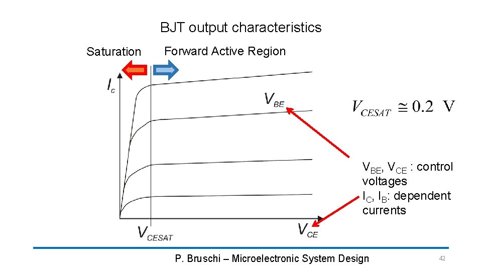
BJT output characteristics Saturation Forward Active Region VBE, VCE : control voltages IC, IB: dependent currents P. Bruschi – Microelectronic System Design 42

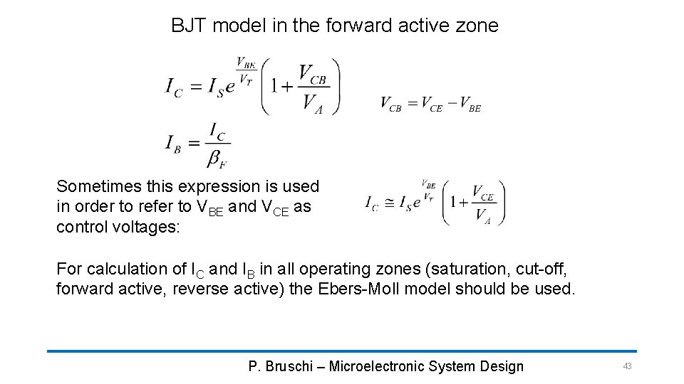
BJT model in the forward active zone Sometimes this expression is used in order to refer to VBE and VCE as control voltages: For calculation of IC and IB in all operating zones (saturation, cut-off, forward active, reverse active) the Ebers-Moll model should be used. P. Bruschi – Microelectronic System Design 43

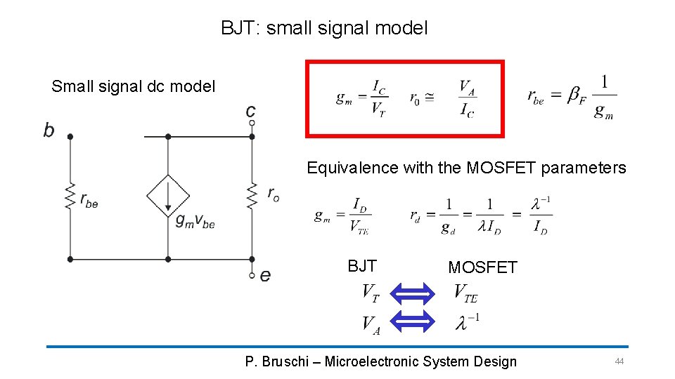
BJT: small signal model Small signal dc model Equivalence with the MOSFET parameters BJT MOSFET P. Bruschi – Microelectronic System Design 44

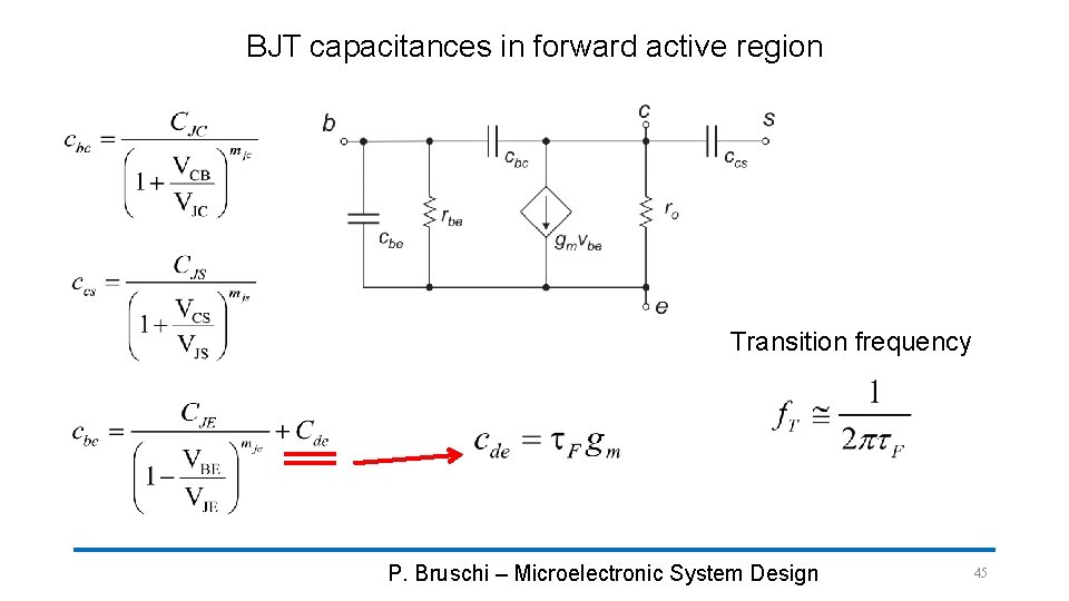
BJT capacitances in forward active region Transition frequency P. Bruschi – Microelectronic System Design 45

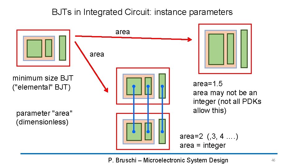
BJTs in Integrated Circuit: instance parameters area minimum size BJT ("elemental" BJT) parameter "area" (dimensionless) area=1. 5 area may not be an integer (not all PDKs allow this) area=2 (, 3, 4 …. ) area = integer P. Bruschi – Microelectronic System Design 46

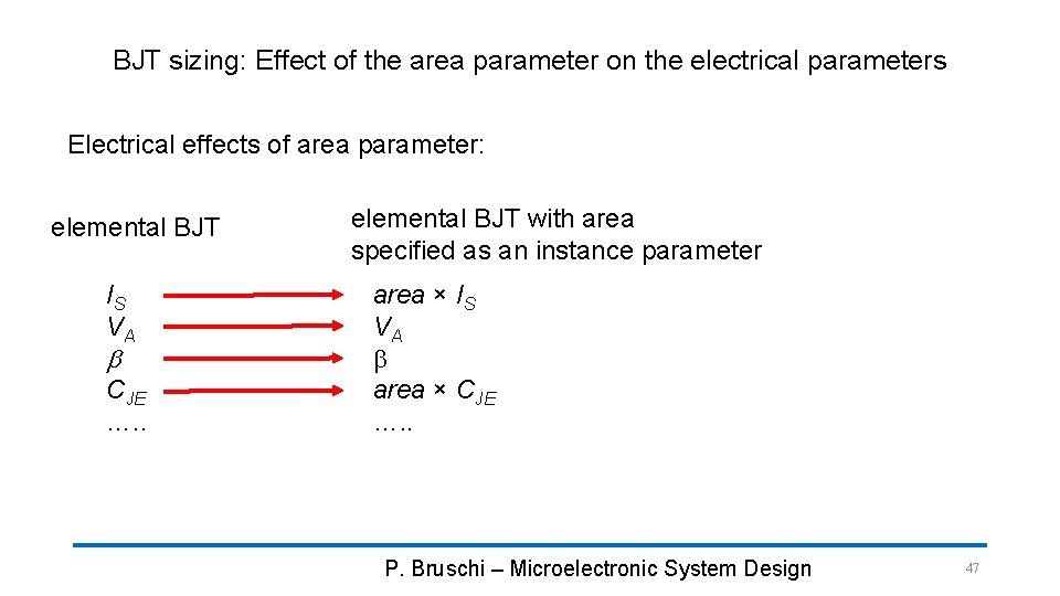
BJT sizing: Effect of the area parameter on the electrical parameters Electrical effects of area parameter: elemental BJT IS VA b CJE …. . elemental BJT with area specified as an instance parameter area × IS VA b area × CJE …. . P. Bruschi – Microelectronic System Design 47

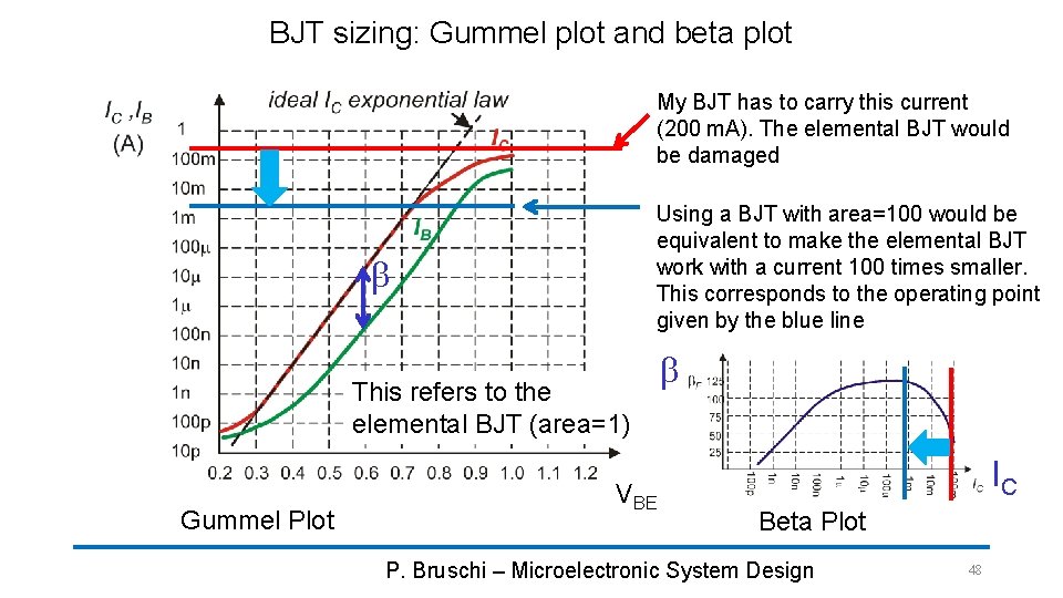
BJT sizing: Gummel plot and beta plot My BJT has to carry this current (200 m. A). The elemental BJT would be damaged Using a BJT with area=100 would be equivalent to make the elemental BJT work with a current 100 times smaller. This corresponds to the operating point given by the blue line b This refers to the elemental BJT (area=1) Gummel Plot VBE b IC Beta Plot P. Bruschi – Microelectronic System Design 48