PIT Programmable Interval Timer Introduction to 82538254 825354

PIT: Programmable Interval Timer Introduction to 8253/8254
 • The 8253 chip")
8253/54 Timer Description and Initialization • PIT (programmable Interval Timer) • The 8253 chip was used in the IBM PC/XT, but starting with the IBM PC/AT, the 8254 replaced the 8253. • 8253 and 8254 have exactly the same pinout. • 8254 is a superset of the 8253.

Programmable Interval Timer 8254

Pin Diagram
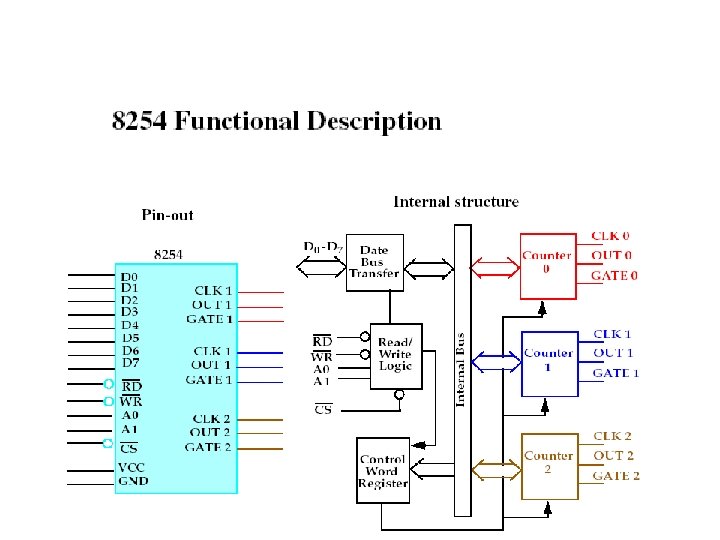

Pin Description of 8253/54 A 0, A 1, and CS • Inside the 8253/54 timer, there are 3 counters. • Each timer works independently and programmed separately. • Each counter is assigned an individual port address. • The control register common to all 3 counters and has its own port.


CLK • CLK is the input clock frequency, which can range between 0 and 2 MHz for the 8253. • For input frequencies higher than 2 MHz, the 8254 must be used. • The 8254 can go as high as 8 MHz, and 8254 -2 can go 10 MHz. OUT • Can have square-wave, one-shot, and other square-shape waves for various duty cycles but no sine-wave or saw-tooth shapes. Gate • This pin is used to enable or disable the counter.

D 0 -D 7 • The D 0 -D 7 data bus of the 8253/54 is a bidirectional bus connected to D 0 -D 7 of the system data bus. • RD and WR are connected to IOR and IOW control signals of the system bus. Initialization of the 8253/54 • Each of the three counters of the 8253/54 must be programmed separately. • The 8253/54 must be initialized before it is used.

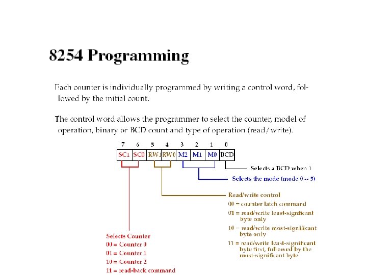
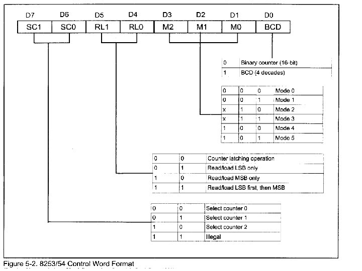


Control word The figure shows the one-byte control word of the 8253/54. • D 0 chooses between a binary number divisor of 0000 to FFFFH or a BCD divisor of 0000 to 9999 H. • The highest number is 216 for binary and 104 for BCD. • To get the highest count, the counter is loaded with zeros. • D 1, D 2, and D 3 are for mode selection.

• D 4 and D 5 are for RL 0 and RL 1 • RL 0 and RL 1 are used to indicate the size of the divisor, and have 3 options: 1. Read/write MSB only 2. Read/write LSB only 3. Read/write LSB first followed immediately by the MSB.

Operation Modes Mode 0 Interrupt on terminal count Mode 1 Programmable one-shot Mode 2 Rate Generator Mode 3 Square wave rate generator Mode 4 Software triggered strobe Mode 5 Hardware trigger strobe

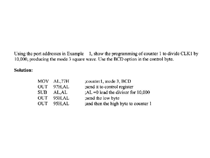
• All counters are down counters. • D 6 and D 7 are used to select the 3 counters, counter 0, counter 1, or counter 2, is to be initialized by the control byte. • To program a given counter of the 8253/54 to divide the CLK input frequency one must send the divisor to that specific counter’s reg. • To divide the frequency by 10000 (BCD) or 65536 (binary) we must send in 0 for both high and low bytes.


IBM PC 8253/54 Timer Connections and Programming

• The three clocks of the 8253, CLK 0, CLK 1, and CLK 2, are all connected to a constant frequency of 1. 1931817 MHz. • PCLK of the 8284 is 2. 3863663 MHz and must be divided by 2. • GATE 0 and GATE 1 enable counter 0 and counter 1 respectively. • GATE 2 of counter 2 can be enabled or disabled through PB 0 of port B of the 8255.
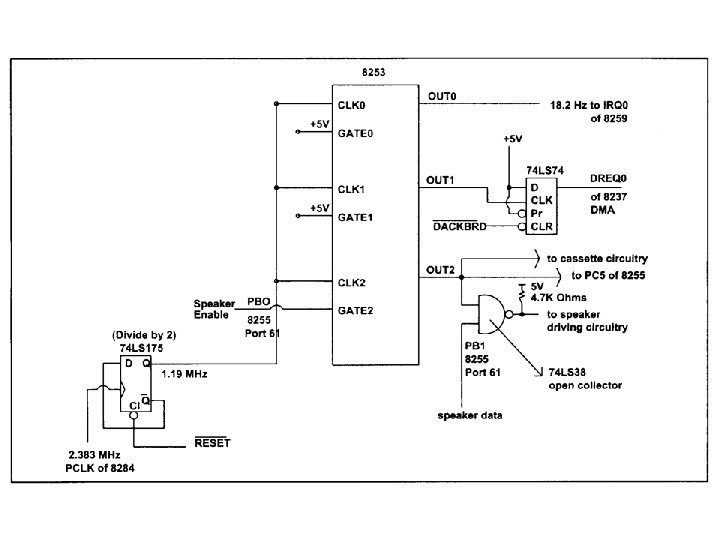

Using counter 0 CLK 0 of counter 0 is 1. 193 MHz, and GATE 0 is connected permanently. • OUT 0 is connected to IRQ 0 of the 8259 interrupt controller to provide time-of-day (TOD) interrupt. • IRQ 0 is activated 18. 2 times per second. (18. 2 Hz) • The counter must to divide 1. 193 MHz by 65, 536.

Using counter 0 • The wave shape is a square wave. • D 0 = 0 for the binary value. • D 3 D 2 D 1 = 011, mode 3 • D 4 D 5 = 11, for reading/writing the LSB first, followed by MSB. • D 7 D 6 = 00, for counter 0.
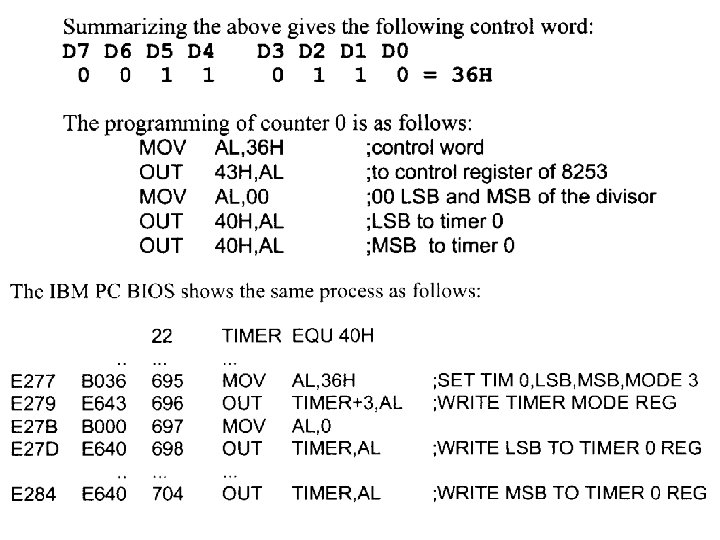

Using counter 0 • The function of IR 0 is not only taking care of the TOD clock. • BIOS will make this interrupt available by going to the vector table of INT 1 CH.

Using Counter 1 • In counter 1, CLK 1 is connected to 1. 193 MHz and GATE is high. • OUT 1 generates a periodic pulse required to refresh DRAM memory of the computer. • The refreshing must be done at least 15 s (66278 Hz) for each cell, and is performed by DMA. • Counter must divide the input frequency 1. 19318 MHz by 18. • DRAM maximum frequency refresh time is 2 ms.

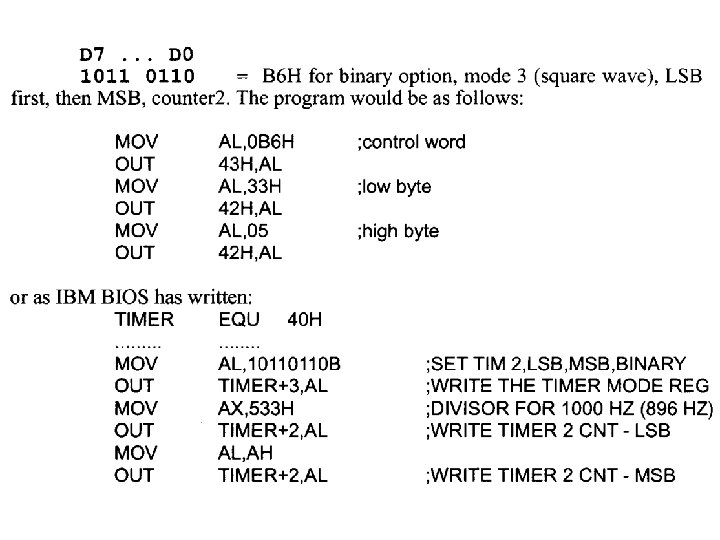
D 0 = 0 for binary option Using Counter 1 D 3 D 2 D 1 = 010, for mode 2 shape output. D 5 D 4 = 01, for LSB only D 7 D 6, for counter 1. D 7~D 0 = 0101 0100 = 54 H for the control word.

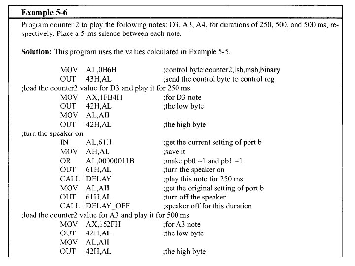
Using Counter 2 The output of counter 2 is connected to two different devices: the speaker and PC 5 of the 8255. Use of timer 2 by the speaker • In the IBM PC, CLK 2 is connected to a frequency of 1. 19318 MHz and GATE 2 is programmed by PB 0 of port 61 H (port B). • The IBM PC uses counter 2 to generate the beep sound. • The beep sound has a frequency of 896 Hz (divisor = 1331)

Turning on the speaker via PB 0 and PB 1 of port 61 H • The process of turning on the speaker is the same for all IBM PCs and compatibles from 8088 -based to 80486 and Intel’s Pentium-based systems. • Gate 2 must be high to provide the CLK to timer 2. • This function is performed by PB 0 of port 61 H. The following is the code to turn the speaker on.

Turning on the speaker via PB 0 and PB 1 of port 61 H

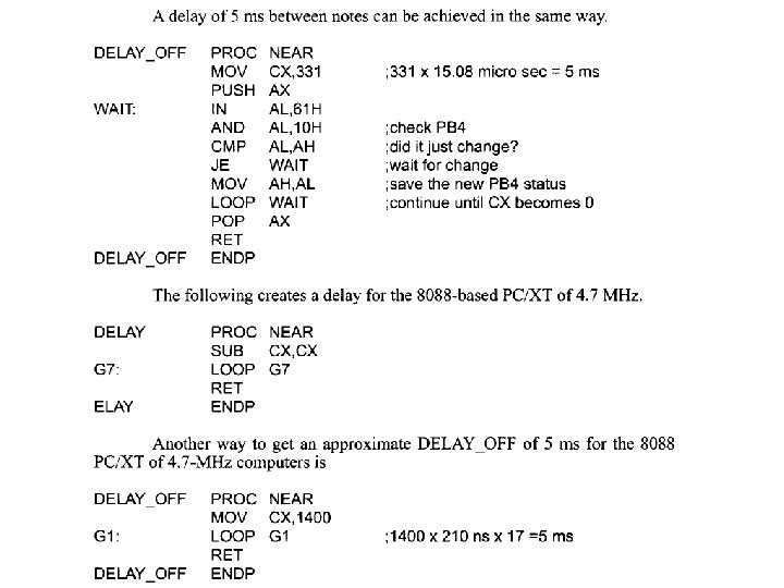
Time delay for 80 x 86 PCs Creating time delays in 8088/86 -based PC/XT, PS 2, and compatibles MOV CX, N AGAIN: LOOP AGAIN The above codes can be used to generate delays (N T 17 seconds) • Approximate delay time • The delay is not only frequency dependent but also CPU dependent. • IBM provides a scheme to create a time delay using hardware that is not only frequency but also CPU independent.

Time delays in 80 x 86 IBM PC The following method of creating hardware time delays was first implemented in the IBM PC and compatible computers. • To create a processor independent delay, IBM made PB 4 of port 61 H toggle every 15. 085 s. • CS holds 15. 085 s in the following codes.

Time delays in 80 x 86 IBM PC

Time delays in 80 x 86 IBM PC • Now a time delay of any duration can be created regardless of the CPU frequency as long as it is a 286 and higher PC. • For example set CX=33144 (33144 15. 085 s=0. 5 second) MOV CX, 33144 CALL WAITF

Time delays in 80 x 86 IBM PC

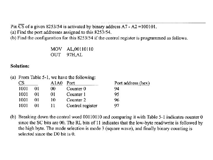
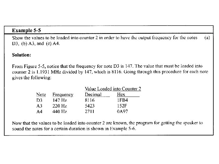
Example

Examples

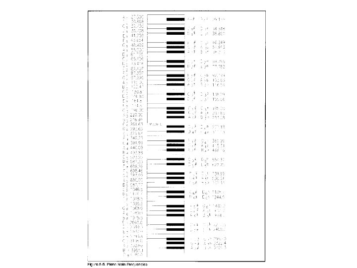
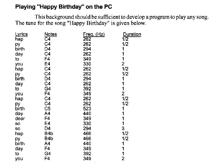
Generating Music on the IBM PC • As mentioned earlier, counter 2 is connected to the speaker and it can be programmed to output any frequency that is desired. • Look at the list of piano notes and their frequencies given in Fig. 5 -5. • Music: frequency and time duration

A delay of 250 ms

Shape of 8253/54 Outputs

Out 0 pulse shape in IBM BIOS programmed counter 0 to create mode 3, which is square-wave shape. • Counter 0 is loaded with the number 65, 536 and the clock period of input frequency 838 ns (1/1. 193 MHz = 838 ns), so the period of the OUT 0 pulse is equal to 65536 838 ns = 54. 9 ms (18. 2 Hz). • OUT 0 continuously sends out square wave pulses.

Out 1 pulse shape in the IBM BIOS programmed counter 1 in mode 2, rate generator, with the value 18 loaded into the counter. • OUT 1 will be high for a total of 17 838 ns and go low for one pulse of 838 ns • GATE 1 is set to 1 permanently

OUT 2 pulse shape in the IBM BIOS loads the value 1331 into counter 2. • Since 1331 is an odd number, the OUT 2 pulse is high for a total of (1331+1)/2 = 666 838 ns and is low for a total of (1331 -1)/2 = 665 838 ns

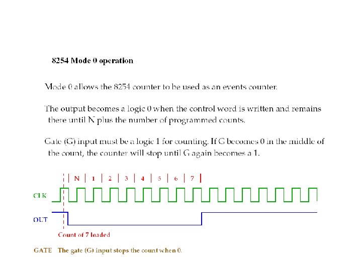
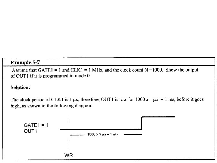
Mode 0: interrupt on terminal count The output in this mode is initially low, and will remain low for the duration of the count if GATE = 1. Width of low pulse = N T Where N is the clock count loaded into counter, and T is the clock period of the CLK input.

Mode 0: interrupt on terminal count When the terminal count is reached, the output will go high and remain high until a new control word or new count number is loaded. • In this mode, if GATE input becomes low at the middle of the count, the count will stop and the output will be low. • The count resumes when the gate becomes high again. • This in effect adds to the total time the output is low.
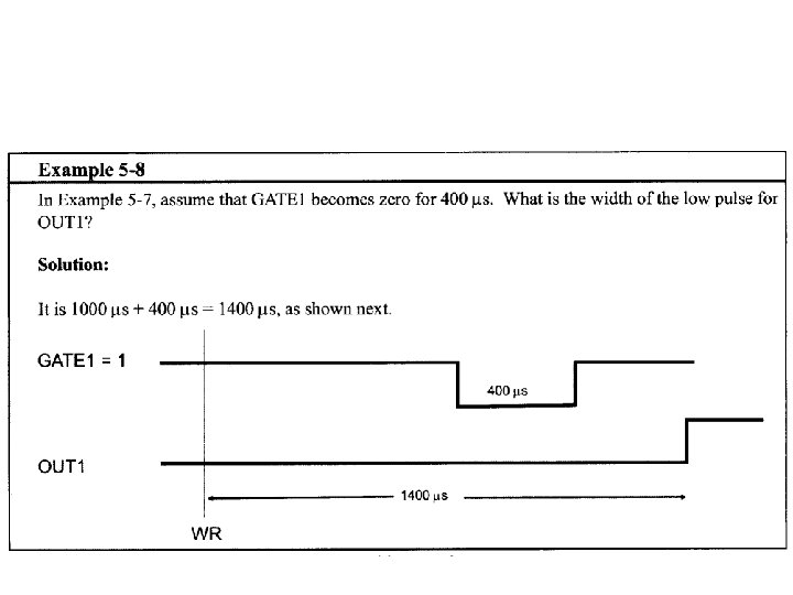

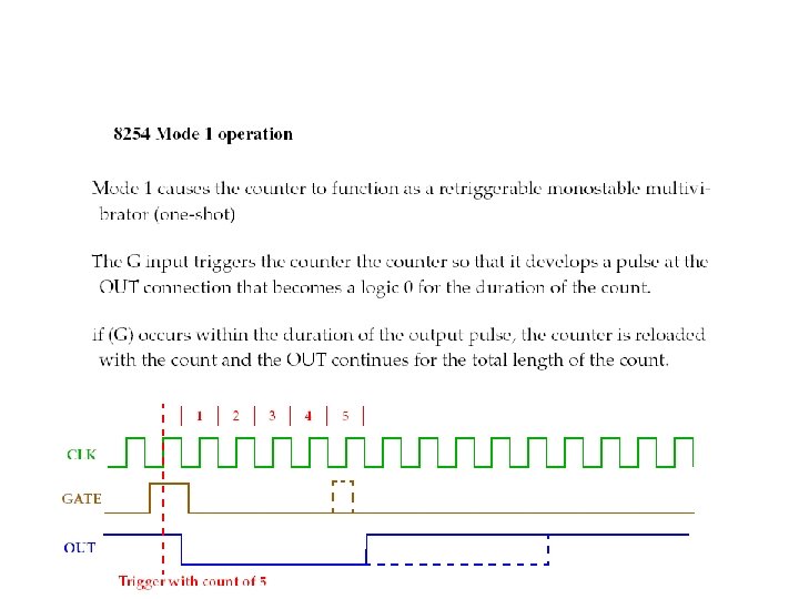
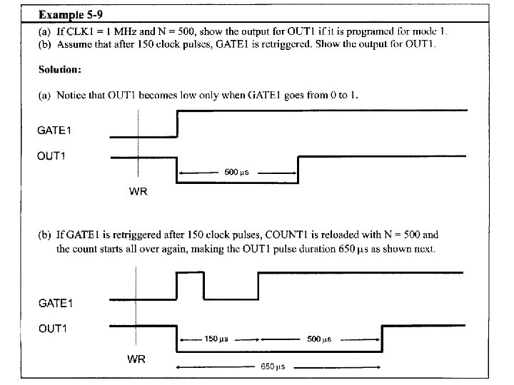
Mode 1: programmable oneshot • This mode is also called hardware triggerable one-shot. • The triggering must be done through the GATE input by sending a 0 -to-1 pulse to it. • The following two steps must be performed: 1. Load the count registers. 2. A 0 -to-1 pulse must be sent to the GATE input to trigger the counter. • Contrast this with mode 0, in which the counter produces the output immediately after the counter is loaded as long as GATE = 1. • In mode 1 after sending the 0 -to-1 pulse to GATE, OUT becomes low and stays low for a duration of N T, then becomes high and stays high until the gate is triggered again.

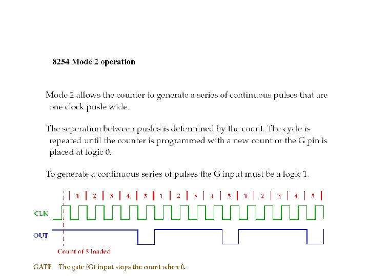
Mode 2: rate generator Mode 2 is also called divide-by-N counter. • In this mode, if GATE = 1, OUT will be high for the N T clock period, goes low for only one clock pulse, then the count is reloaded automatically, and the process continues indefinitely.

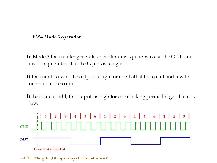
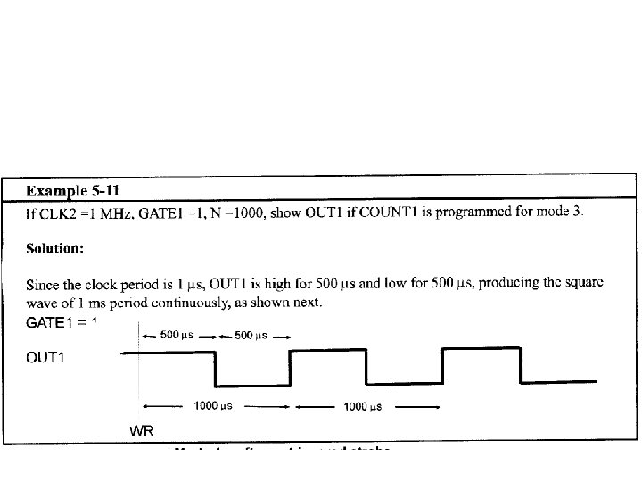
Mode 3: square wave rate generator In this mode if GATE = 1, OUT is a square wave where the high pulse is equal to the low pulse if N is an even number. • In this case the high part and low part of the pulse have the same duration and are equal to (N/2) T (50% duty cycle) • If N is an odd number, the high pulse is one clock pulse longer. • This mode is widely used as a frequency divider and audio-tone generator.

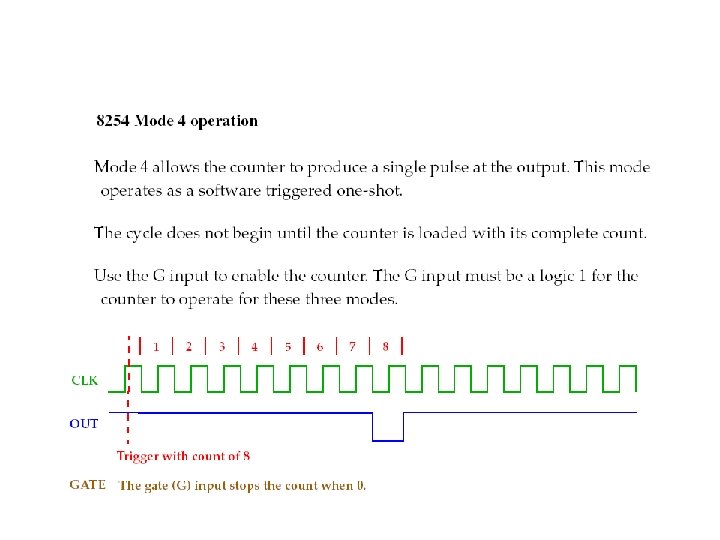
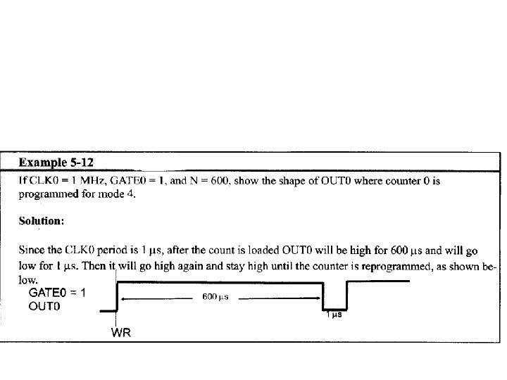
Mode 4: software trigger strobe • In this mode if GATE = 1, the output will go high upon loading the count. • It will stay high for the duration of N T. • After the count reaches zero (terminal count), it becomes low for one clock pulse, then goes high again and stays high until a new command word or new count is loaded. • To repeat the strobe, the count must be reloaded again. • Mode 4 is similar to mode 2, except that the counter is not reloaded automatically. • In this mode, the count starts the moment the count is written into the counter.
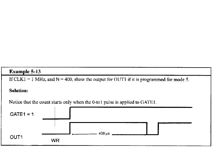

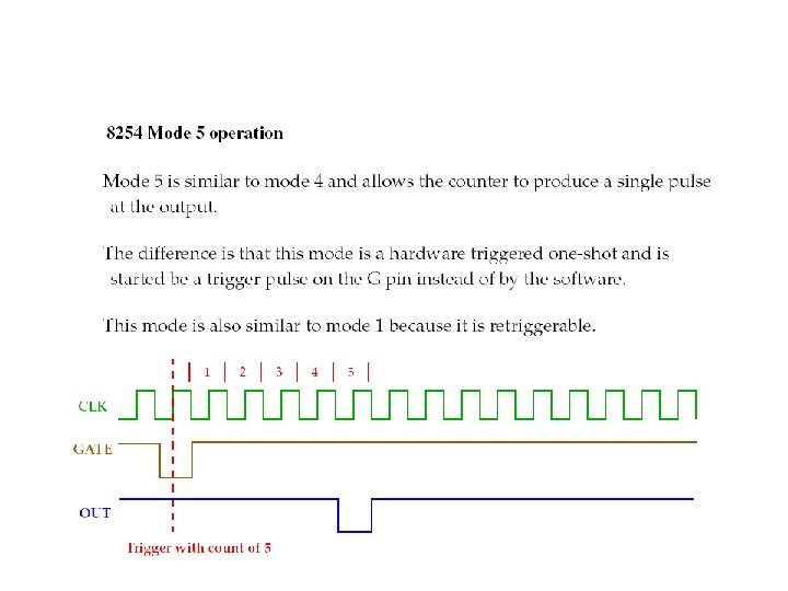
Mode 5: hardware trigger strobe • This mode is similar to mode 4 except that the trigger must be done with the GATE input. • In this mode after the count is loaded, we must send a low-to-high puls to the gate to start the counter.
- Slides: 71