PIP 2 LCLK Preliminary Design Review LCLKII Preliminary

- Slides: 18

PIP 2 LCLK Preliminary Design Review LCLK-II Preliminary Hardware Design Mark Austin AD/Controls 1 September 2020 A Partnership of: US/DOE India/DAE Italy/INFN UK/UKRI-STFC France/CEA, CNRS/IN 2 P 3 Poland/WUST

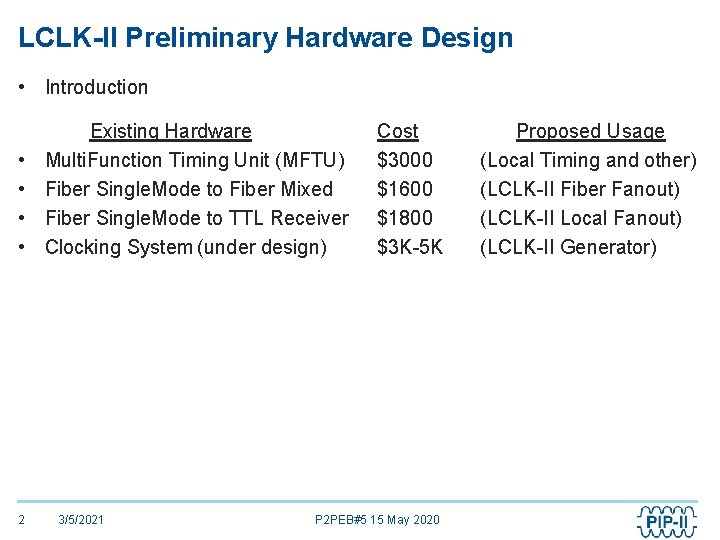
LCLK-II Preliminary Hardware Design • Introduction • • 2 Existing Hardware Multi. Function Timing Unit (MFTU) Fiber Single. Mode to Fiber Mixed Fiber Single. Mode to TTL Receiver Clocking System (under design) 3/5/2021 Cost $3000 $1600 $1800 $3 K-5 K P 2 PEB#5 15 May 2020 Proposed Usage (Local Timing and other) (LCLK-II Fiber Fanout) (LCLK-II Local Fanout) (LCLK-II Generator)

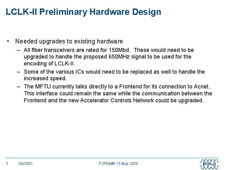
LCLK-II Preliminary Hardware Design • Needed upgrades to existing hardware – All fiber transceivers are rated for 150 Mbd. These would need to be upgraded to handle the proposed 650 MHz signal to be used for the encoding of LCLK-II. – Some of the various ICs would need to be replaced as well to handle the increased speed. – The MFTU currently talks directly to a Frontend for its connection to Acnet. This interface could remain the same while the communication between the Frontend and the new Accelerator Controls Network could be upgraded. 3 3/5/2021 P 2 PEB#5 15 May 2020

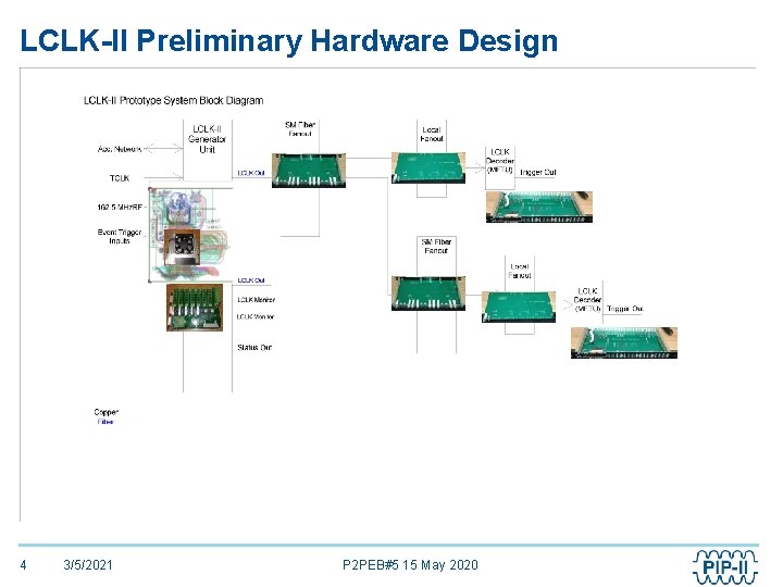
LCLK-II Preliminary Hardware Design 4 3/5/2021 P 2 PEB#5 15 May 2020

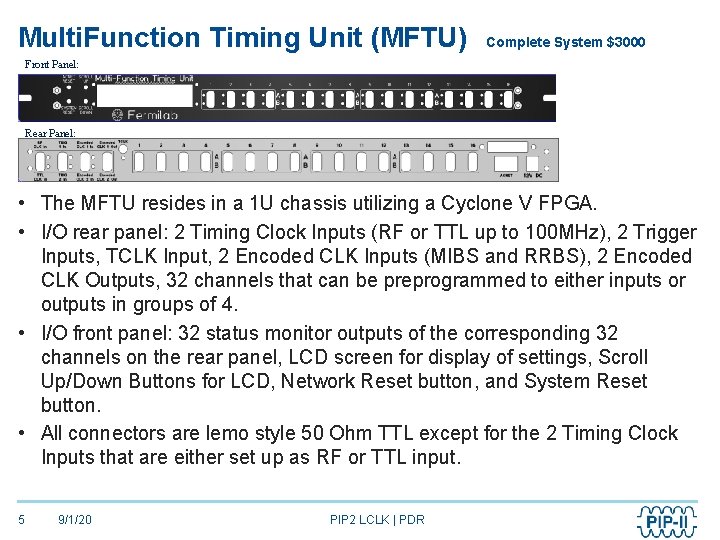
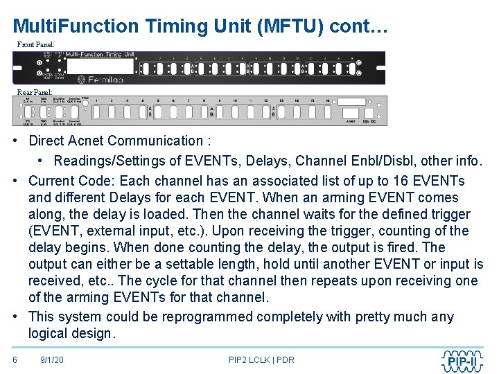
Multi. Function Timing Unit (MFTU) Complete System $3000 Front Panel: Rear Panel: • The MFTU resides in a 1 U chassis utilizing a Cyclone V FPGA. • I/O rear panel: 2 Timing Clock Inputs (RF or TTL up to 100 MHz), 2 Trigger Inputs, TCLK Input, 2 Encoded CLK Inputs (MIBS and RRBS), 2 Encoded CLK Outputs, 32 channels that can be preprogrammed to either inputs or outputs in groups of 4. • I/O front panel: 32 status monitor outputs of the corresponding 32 channels on the rear panel, LCD screen for display of settings, Scroll Up/Down Buttons for LCD, Network Reset button, and System Reset button. • All connectors are lemo style 50 Ohm TTL except for the 2 Timing Clock Inputs that are either set up as RF or TTL input. 5 9/1/20 PIP 2 LCLK | PDR

Multi. Function Timing Unit (MFTU) cont… Front Panel: Rear Panel: • Direct Acnet Communication : • Readings/Settings of EVENTs, Delays, Channel Enbl/Disbl, other info. • Current Code: Each channel has an associated list of up to 16 EVENTs and different Delays for each EVENT. When an arming EVENT comes along, the delay is loaded. Then the channel waits for the defined trigger (EVENT, external input, etc. ). Upon receiving the trigger, counting of the delay begins. When done counting the delay, the output is fired. The output can either be a settable length, hold until another EVENT or input is received, etc. . The cycle for that channel then repeats upon receiving one of the arming EVENTs for that channel. • This system could be reprogrammed completely with pretty much any logical design. 6 9/1/20 PIP 2 LCLK | PDR

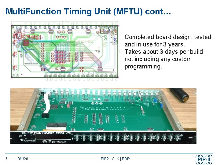
Multi. Function Timing Unit (MFTU) cont… Completed board design, tested and in use for 3 years. Takes about 3 days per build not including any custom programming. 7 9/1/20 PIP 2 LCLK | PDR

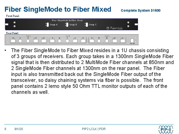
Fiber Single. Mode to Fiber Mixed Complete System $1600 Front Panel: Rear Panel: • The Fiber Single. Mode to Fiber Mixed resides in a 1 U chassis consisting of 3 groups of receivers. Each group takes in a 1300 nm Single. Mode Fiber signal that is then distributed to 2 Multi. Mode Fiber channels at 850 nm and 2 Single. Mode Fiber channels at 1300 nm on the rear panel. The Fiber input is also transmitted back out the Single. Mode Fiber output of the transceiver, so daisy chaining systems via fiber is possible. The front panel contains 2 lemo style 50 Ohm TTL monitor outputs of each of the channels as well. 8 9/1/20 PIP 2 LCLK | PDR

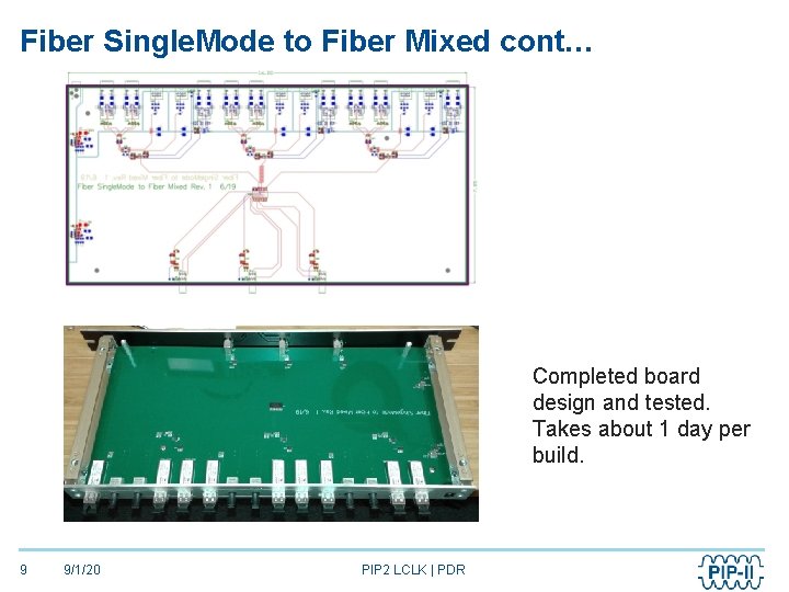
Fiber Single. Mode to Fiber Mixed cont… Completed board design and tested. Takes about 1 day per build. 9 9/1/20 PIP 2 LCLK | PDR

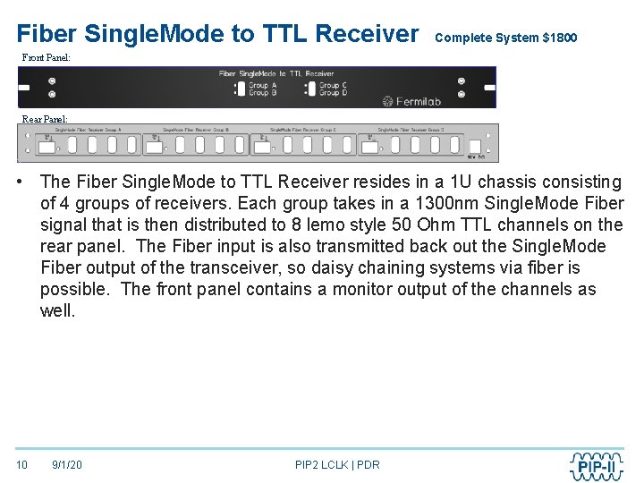
Fiber Single. Mode to TTL Receiver Complete System $1800 Front Panel: Rear Panel: • The Fiber Single. Mode to TTL Receiver resides in a 1 U chassis consisting of 4 groups of receivers. Each group takes in a 1300 nm Single. Mode Fiber signal that is then distributed to 8 lemo style 50 Ohm TTL channels on the rear panel. The Fiber input is also transmitted back out the Single. Mode Fiber output of the transceiver, so daisy chaining systems via fiber is possible. The front panel contains a monitor output of the channels as well. 10 9/1/20 PIP 2 LCLK | PDR

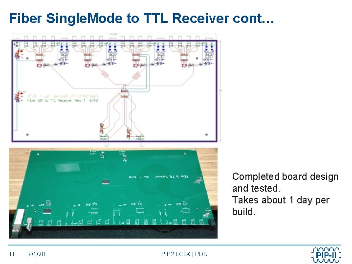
Fiber Single. Mode to TTL Receiver cont… Completed board design and tested. Takes about 1 day per build. 11 9/1/20 PIP 2 LCLK | PDR

Clocking System Complete System $3000 - $5000 • The Clocking System consists of a 4 U chassis (half or full depth) with a 12 V 650 W internal power supply. This supply feeds the Power Supply Board (Pwr. Board) which in turn feeds the Base. Board. The Baseboard is then used to interface with riser cards, front panel cards, or back panel cards, etc. that can be quickly produced since they will contain significantly less components. The chassis also contains cooling fans for the system. 12 9/1/20 PIP 2 LCLK | PDR

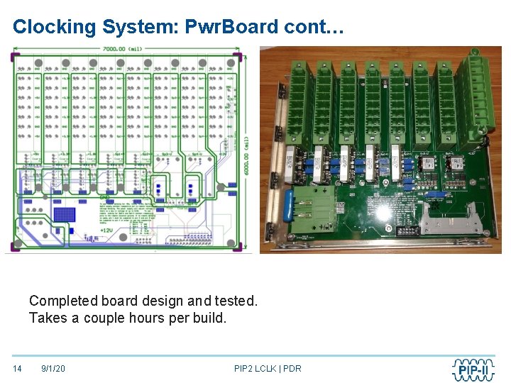
Clocking System: Pwr. Board Cost of only Pwr. Board $500 • The Pwr. Board contains a connector with up to 4 different screw terminal connections for each of the following supplies: 12 V, 5 V, 3. 3 V, 1. 8 V, 2 manually adjustable positive supplies settable from 0. 6 V to 5 V, as well as 2 manually adjustable negative supplies settable from -3. 3 V to -30 V. The positive supplies are capable of up to 200 W each and the negative supplies are capable of up to 75 W each given that the total of all supplies cannot exceed the total 650 W main supply. • Each supply can be monitored for appropriate voltage and each supply can be independently enabled or disabled (except the 12 V supply; if it is off, the FPGA is powered down). The positive power supplies also have remote sensing pins that can be wired to other locations. This allows the power supply to automatically adjust the voltage if there is a small voltage drop at the remote location. 13 9/1/20 PIP 2 LCLK | PDR

Clocking System: Pwr. Board cont… Completed board design and tested. Takes a couple hours per build. 14 9/1/20 PIP 2 LCLK | PDR

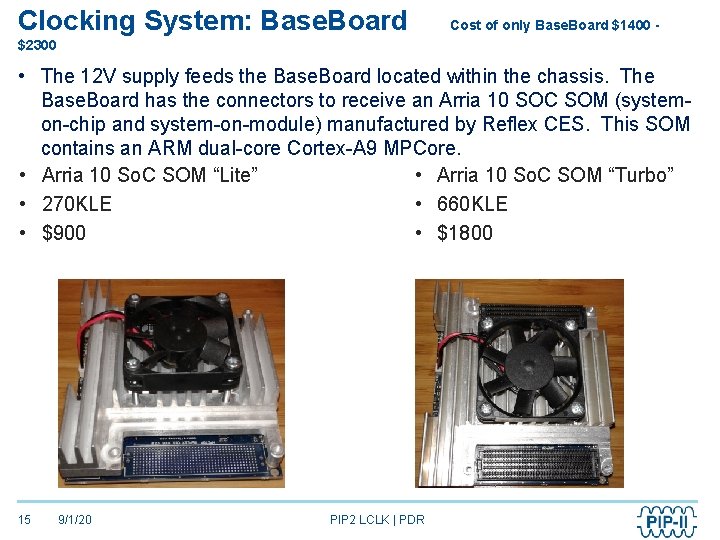
Clocking System: Base. Board Cost of only Base. Board $1400 - $2300 • The 12 V supply feeds the Base. Board located within the chassis. The Base. Board has the connectors to receive an Arria 10 SOC SOM (systemon-chip and system-on-module) manufactured by Reflex CES. This SOM contains an ARM dual-core Cortex-A 9 MPCore. • Arria 10 So. C SOM “Lite” • Arria 10 So. C SOM “Turbo” • 270 KLE • 660 KLE • $900 • $1800 15 9/1/20 PIP 2 LCLK | PDR

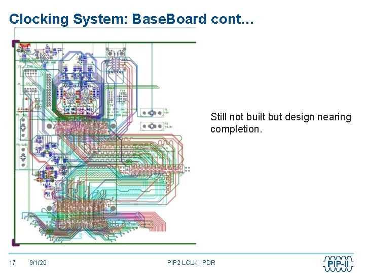
Clocking System: Base. Board cont… • I/O rear panel: USB 3. 0 connector, USB connector for connection to the hard processor system and the MAX 10 on the board, USB-OTG, JTAG connector, 2 ethernet-RJ 45 connectors, 4 SFP+ connectors for fiber transceivers. • I/O internal: I 2 C/SPI, PMBUS, FX 3 (not available with “Lite” SOM), as well as 2 Off-Board connectors that each contain 10 transceivers and 40 LVDS pairs. • These two Off-Board connectors are meant to be used for connecting to yet to be designed riser cards, front panel cards, or back panel cards that will reside within the chassis and be powered by the other connections available on the Pwr. Board. All transceiver channels and LVDS pairs are 100 Ohm impedance and all traces for each connector have been tuned to all have a matched trace length from the FPGA on the SOM to the Off. Board connector. • The Off-Board connectors and FPGA really allow this system to be used in many different applications by quickly designing other cards and programming the desired functionality for the hardware in the FPGA. 16 9/1/20 PIP 2 LCLK | PDR

Clocking System: Base. Board cont… Still not built but design nearing completion. 17 9/1/20 PIP 2 LCLK | PDR

Thank you! 18 9/1/20 PIP 2 LCLK | PDR