Picosecond time measurement using ultra fast analog memories

- Slides: 28

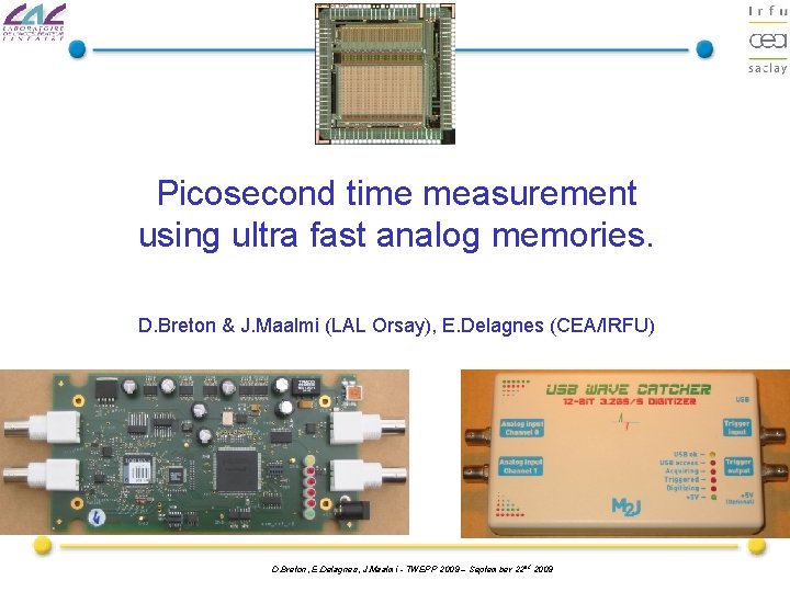
Picosecond time measurement using ultra fast analog memories. D. Breton & J. Maalmi (LAL Orsay), E. Delagnes (CEA/IRFU) D. Breton, E. Delagnes, J. Maalmi - TWEPP 2009 – September 22 nd 2009

History of the Orsay/Saclay SCA Developments • The story begins in 1992 with the design of the first prototype of the Switched Capacitor Array (SCA) for the ATLAS LARG calorimeter. After 10 years of development, the main final characteristics of this rad-hard circuit were: • 12 pseudo-differential channels • 40 MHz sampling • 13. 6 -bit dynamic range with simultaneous write/read • 80000 chips produced in 2002 and mounted on the detector. • Since 2002, 3 new generations of fast samplers have been designed (ARS, MATACQ, SAM): total of more than 30000 chips in use. • Our design philosophy: 1. Maximize dynamic range and minimize signal distorsion. 2. Minimize need for calibrations and off-chip data corrections. 3. Minimize costs (both for development & production): • Use of inexpensive pure CMOS technologies (0. 8µm then 0. 35µm); • Use of packaged chips (cheap QFP). D. Breton, E. Delagnes, J. Maalmi - TWEPP 2009 – September 22 nd 2009

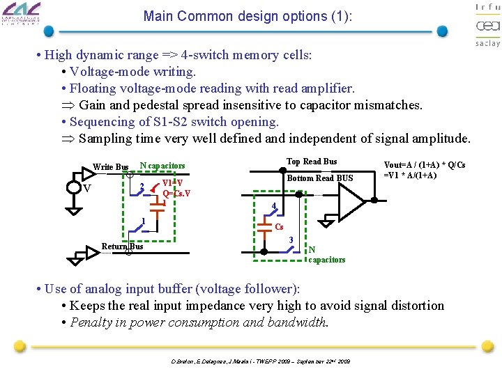
Main Common design options (1): • High dynamic range => 4 -switch memory cells: • Voltage-mode writing. • Floating voltage-mode reading with read amplifier. Þ Gain and pedestal spread insensitive to capacitor mismatches. • Sequencing of S 1 -S 2 switch opening. Þ Sampling time very well defined and independent of signal amplitude. Write Bus v Top Read Bus N capacitors 2 1 Return Bus V 1=V Q=Cs. V 1 Bottom Read BUS Vout=A / (1+A) * Q/Cs =V 1 * A/(1+A) 4 Cs 3 N capacitors • Use of analog input buffer (voltage follower): • Keeps the real input impedance very high to avoid signal distortion • Penalty in power consumption and bandwidth. D. Breton, E. Delagnes, J. Maalmi - TWEPP 2009 – September 22 nd 2009

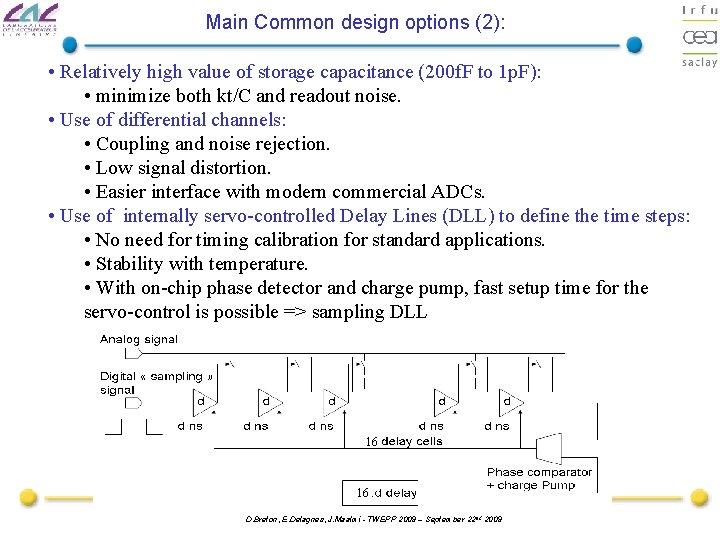
Main Common design options (2): • Relatively high value of storage capacitance (200 f. F to 1 p. F): • minimize both kt/C and readout noise. • Use of differential channels: • Coupling and noise rejection. • Low signal distortion. • Easier interface with modern commercial ADCs. • Use of internally servo-controlled Delay Lines (DLL) to define the time steps: • No need for timing calibration for standard applications. • Stability with temperature. • With on-chip phase detector and charge pump, fast setup time for the servo-control is possible => sampling DLL 16 16 D. Breton, E. Delagnes, J. Maalmi - TWEPP 2009 – September 22 nd 2009

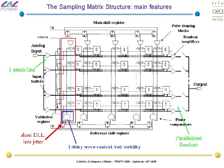
The Sampling Matrix Structure: main features D. Breton, E. Delagnes, J. Maalmi - TWEPP 2009 – September 22 nd 2009

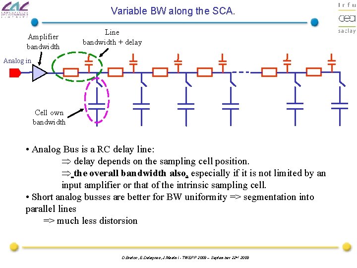
Variable BW along the SCA. Amplifier bandwidth Line bandwidth + delay Analog in Cell own bandwidth • Analog Bus is a RC delay line: Þ delay depends on the sampling cell position. Þ the overall bandwidth also, especially if it is not limited by an input amplifier or that of the intrinsic sampling cell. • Short analog busses are better for BW uniformity => segmentation into parallel lines => much less distorsion D. Breton, E. Delagnes, J. Maalmi - TWEPP 2009 – September 22 nd 2009

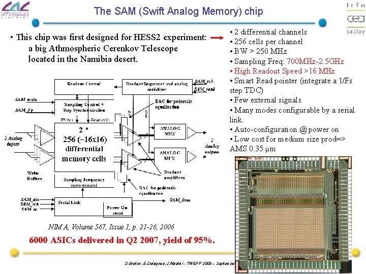
The SAM (Swift Analog Memory) chip • This chip was first designed for HESS 2 experiment: a big Athmospheric Cerenkov Telescope located in the Namibia desert. • 2 differential channels • 256 cells per channel • BW > 250 MHz • Sampling Freq: 700 MHz-2. 5 GHz • High Readout Speed >16 MHz • Smart Read pointer (integrate a 1/Fs step TDC) • Few external signals • Many modes configurable by a serial link. • Auto-configuration @ power on • Low cost for medium size prod=> AMS 0. 35 µm NIM A, Volume 567, Issue 1, p. 21 -26, 2006 6000 ASICs delivered in Q 2 2007, yield of 95%. D. Breton, E. Delagnes, J. Maalmi - TWEPP 2009 – September 22 nd 2009

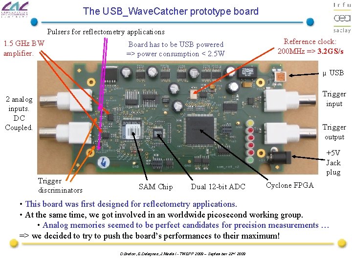
The USB_Wave. Catcher prototype board Pulsers for reflectometry applications 1. 5 GHz BW amplifier. Board has to be USB powered => power consumption < 2. 5 W Reference clock: 200 MHz => 3. 2 GS/s µ USB Trigger input 2 analog inputs. DC Coupled. Trigger output +5 V Jack plug Trigger discriminators SAM Chip Dual 12 -bit ADC Cyclone FPGA • This board was first designed for reflectometry applications. • At the same time, we got involved in an worldwide picosecond working group. • Analog memories seemed to be perfect candidates for precision measurements … => we decided to try to push the board’s performances to their maximum! D. Breton, E. Delagnes, J. Maalmi - TWEPP 2009 – September 22 nd 2009

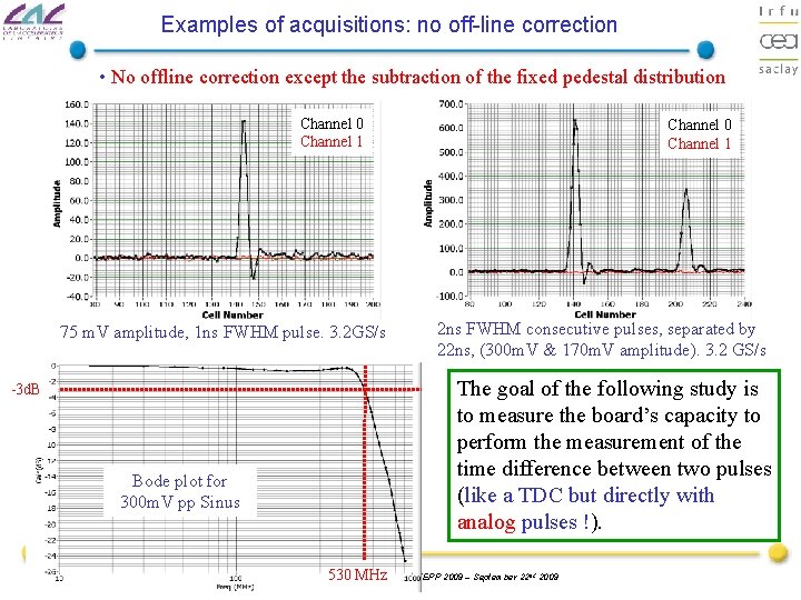
Examples of acquisitions: no off-line correction • No offline correction except the subtraction of the fixed pedestal distribution Channel 0 Channel 1 75 m. V amplitude, 1 ns FWHM pulse. 3. 2 GS/s Channel 0 Channel 1 2 ns FWHM consecutive pulses, separated by 22 ns, (300 m. V & 170 m. V amplitude). 3. 2 GS/s The goal of the following study is to measure the board’s capacity to perform the measurement of the time difference between two pulses (like a TDC but directly with analog pulses !). -3 d. B Bode plot for 300 m. V pp Sinus 530 MHz D. Breton, E. Delagnes, J. Maalmi - TWEPP 2009 – September 22 nd 2009

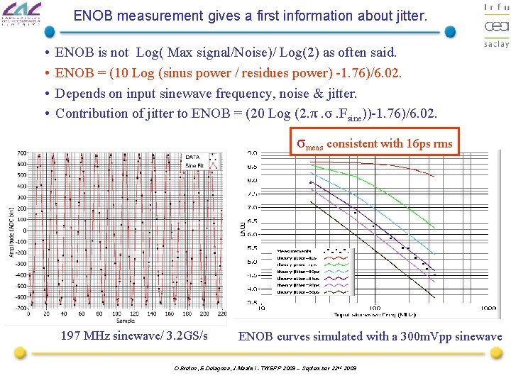
ENOB measurement gives a first information about jitter. • • ENOB is not Log( Max signal/Noise)/ Log(2) as often said. ENOB = (10 Log (sinus power / residues power) -1. 76)/6. 02. Depends on input sinewave frequency, noise & jitter. Contribution of jitter to ENOB = (20 Log (2. π. σ. Fsine))-1. 76)/6. 02. σmeas consistent with 16 ps rms 197 MHz sinewave/ 3. 2 GS/s ENOB curves simulated with a 300 m. Vpp sinewave D. Breton, E. Delagnes, J. Maalmi - TWEPP 2009 – September 22 nd 2009

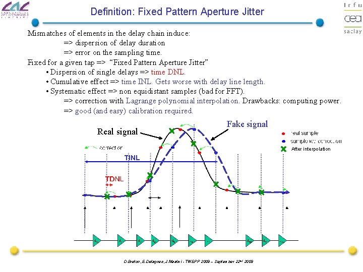
Definition: Fixed Pattern Aperture Jitter Mismatches of elements in the delay chain induce: => dispersion of delay duration => error on the sampling time. Fixed for a given tap => “Fixed Pattern Aperture Jitter” • Dispersion of single delays => time DNL. • Cumulative effect => time INL. Gets worse with delay line length. • Systematic effect => non equidistant samples (bad for FFT). => correction with Lagrange polynomial interpolation. Drawbacks: computing power. => good (and easy) calibration required. Real signal Fake signal After interpolation D. Breton, E. Delagnes, J. Maalmi - TWEPP 2009 – September 22 nd 2009

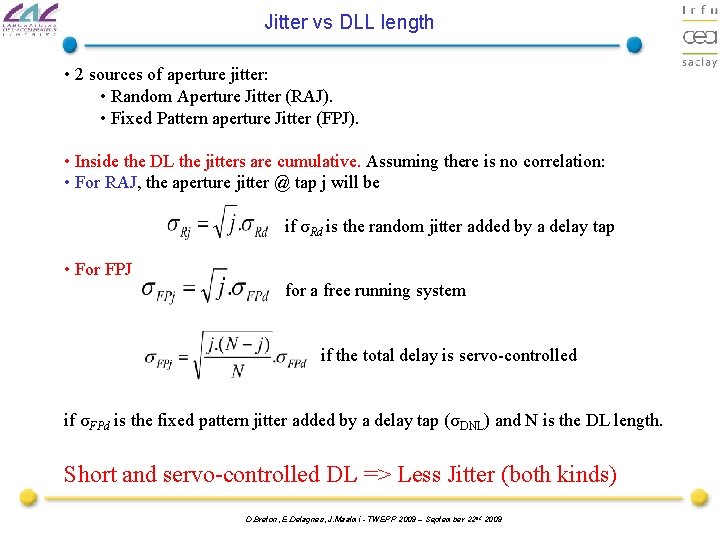
Jitter vs DLL length • 2 sources of aperture jitter: • Random Aperture Jitter (RAJ). • Fixed Pattern aperture Jitter (FPJ). • Inside the DL the jitters are cumulative. Assuming there is no correlation: • For RAJ, the aperture jitter @ tap j will be if σRd is the random jitter added by a delay tap • For FPJ for a free running system if the total delay is servo-controlled if σFPd is the fixed pattern jitter added by a delay tap (σDNL) and N is the DL length. Short and servo-controlled DL => Less Jitter (both kinds) D. Breton, E. Delagnes, J. Maalmi - TWEPP 2009 – September 22 nd 2009

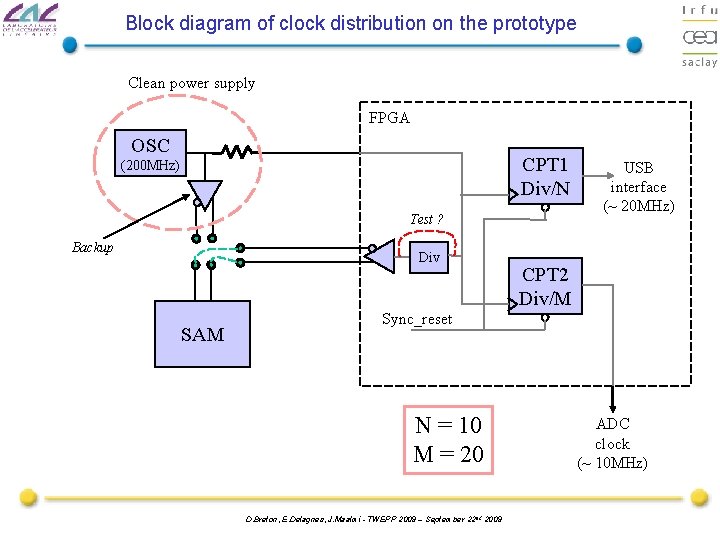
Block diagram of clock distribution on the prototype Clean power supply FPGA OSC CPT 1 Div/N (200 MHz) Test ? Backup Div SAM USB interface (~ 20 MHz) CPT 2 Div/M Sync_reset N = 10 M = 20 D. Breton, E. Delagnes, J. Maalmi - TWEPP 2009 – September 22 nd 2009 ADC clock (~ 10 MHz)

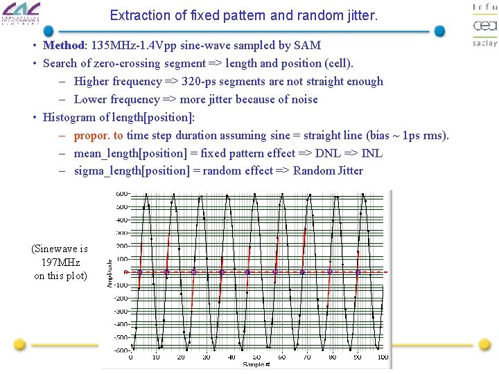
Extraction of fixed pattern and random jitter. • Method: 135 MHz-1. 4 Vpp sine-wave sampled by SAM • Search of zero-crossing segment => length and position (cell). – Higher frequency => 320 -ps segments are not straight enough – Lower frequency => more jitter because of noise • Histogram of length[position]: – propor. to time step duration assuming sine = straight line (bias ~ 1 ps rms). – mean_length[position] = fixed pattern effect => DNL => INL – sigma_length[position] = random effect => Random Jitter (Sinewave is 197 MHz on this plot) D. Breton, E. Delagnes, J. Maalmi - TWEPP 2009 – September 22 nd 2009

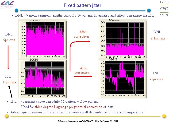
Fixed pattern jitter • DNL => mean segment lengths. Modulo 16 pattern. Integrated and fitted to measure the INL. DNL 9 ps rms INL 16 ps rms After correction DNL 2. 1 ps rms INL ~1 ps rms • INL => segments have a modulo 16 pattern + slow pattern. – Used for third degree Lagrange polynomial correction of data • Advantage of servo-controlled structure: very small dependence to time and temperature D. Breton, E. Delagnes, J. Maalmi - TWEPP 2009 – September 22 nd 2009

Random jitter After correction • Very encouraging random jitter floor ~ 2 ps rms • But peaks on “transition” samples up to ~20 ps (mean jitter ~3 ps) – Understood: due to the clock jitter, which can be seen only on the last cell of the DLLs – The oscillator is supposed to deliver a clean clock = > probable source: the FPGA D. Breton, E. Delagnes, J. Maalmi - TWEPP 2009 – September 22 nd 2009

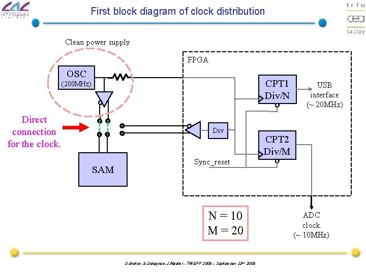
First block diagram of clock distribution Clean power supply FPGA OSC CPT 1 Div/N (200 MHz) Direct connection for the clock. Div SAM USB interface (~ 20 MHz) CPT 2 Div/M Sync_reset N = 10 M = 20 D. Breton, E. Delagnes, J. Maalmi - TWEPP 2009 – September 22 nd 2009 ADC clock (~ 10 MHz)

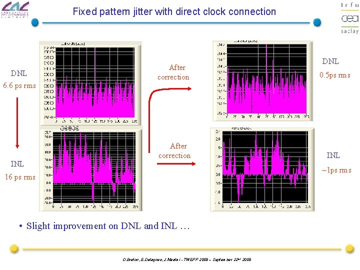
Fixed pattern jitter with direct clock connection DNL 6. 6 ps rms INL DNL After correction 0. 5 ps rms After correction INL ~1 ps rms 16 ps rms • Slight improvement on DNL and INL … D. Breton, E. Delagnes, J. Maalmi - TWEPP 2009 – September 22 nd 2009

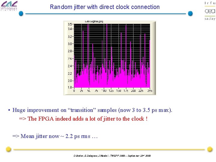
Random jitter with direct clock connection • Huge improvement on “transition” samples (now 3 to 3. 5 ps max). => The FPGA indeed adds a lot of jitter to the clock ! => Mean jitter now ~ 2. 2 ps rms … D. Breton, E. Delagnes, J. Maalmi - TWEPP 2009 – September 22 nd 2009

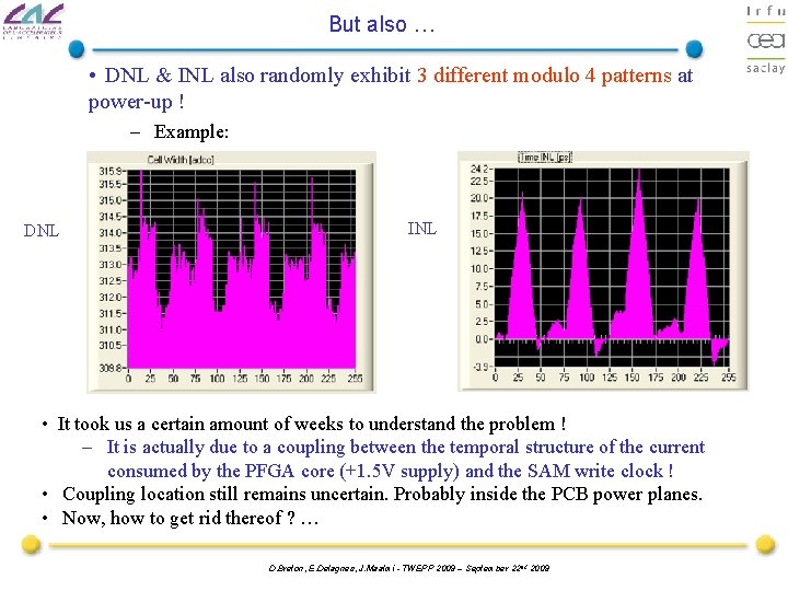
But also … • DNL & INL also randomly exhibit 3 different modulo 4 patterns at power-up ! – Example: DNL INL • It took us a certain amount of weeks to understand the problem ! – It is actually due to a coupling between the temporal structure of the current consumed by the PFGA core (+1. 5 V supply) and the SAM write clock ! • Coupling location still remains uncertain. Probably inside the PCB power planes. • Now, how to get rid thereof ? … D. Breton, E. Delagnes, J. Maalmi - TWEPP 2009 – September 22 nd 2009

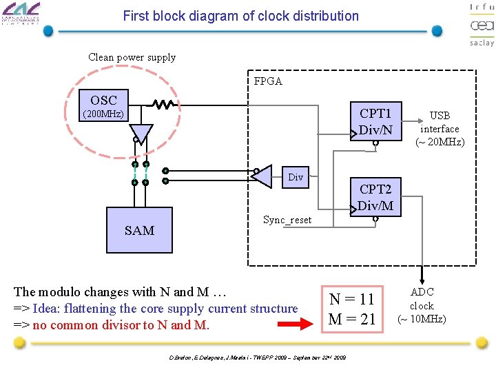
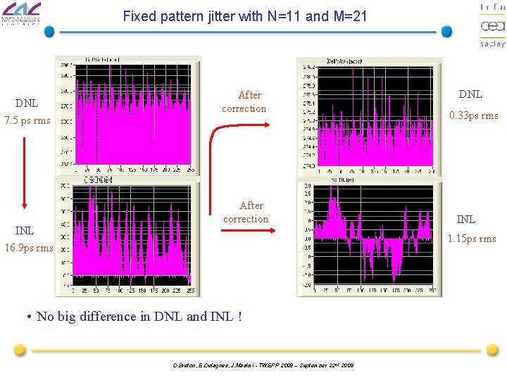
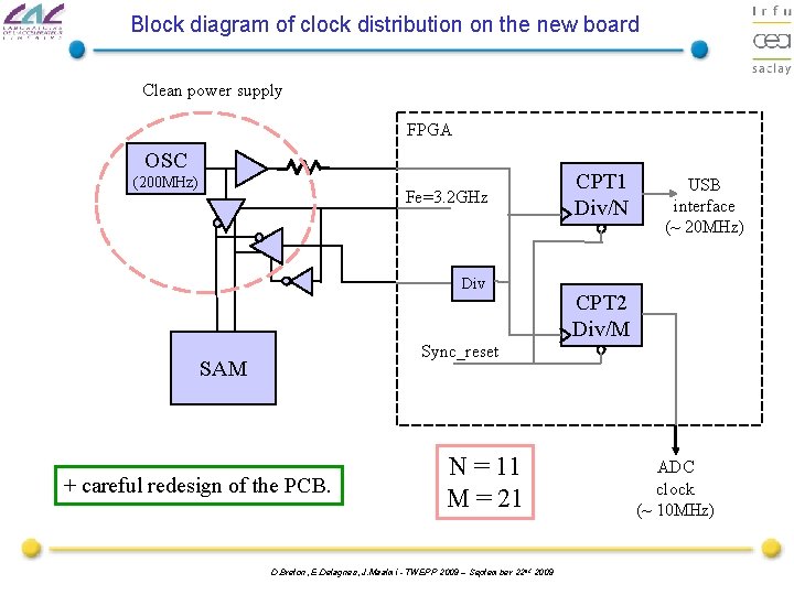
First block diagram of clock distribution Clean power supply FPGA OSC CPT 1 Div/N (200 MHz) Div SAM USB interface (~ 20 MHz) CPT 2 Div/M Sync_reset The modulo changes with N and M … => Idea: flattening the core supply current structure => no common divisor to N and M. N = 11 M = 21 D. Breton, E. Delagnes, J. Maalmi - TWEPP 2009 – September 22 nd 2009 ADC clock (~ 10 MHz)

Fixed pattern jitter with N=11 and M=21 DNL 7. 5 ps rms INL 16. 9 ps rms After correction DNL 0. 33 ps rms INL 1. 15 ps rms • No big difference in DNL and INL ! D. Breton, E. Delagnes, J. Maalmi - TWEPP 2009 – September 22 nd 2009

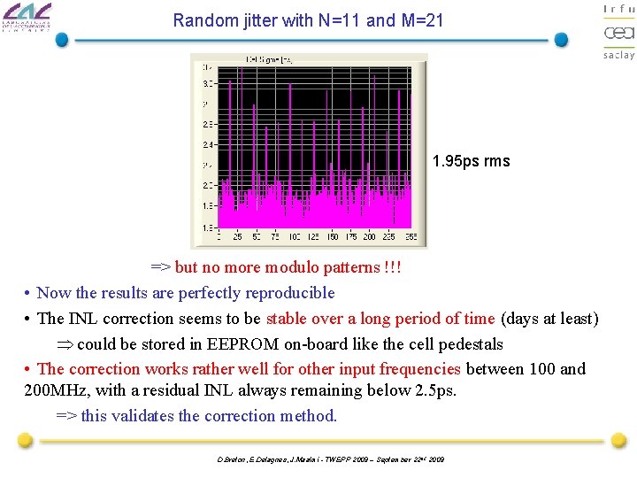
Random jitter with N=11 and M=21 1. 95 ps rms => but no more modulo patterns !!! • Now the results are perfectly reproducible • The INL correction seems to be stable over a long period of time (days at least) Þ could be stored in EEPROM on-board like the cell pedestals • The correction works rather well for other input frequencies between 100 and 200 MHz, with a residual INL always remaining below 2. 5 ps. => this validates the correction method. D. Breton, E. Delagnes, J. Maalmi - TWEPP 2009 – September 22 nd 2009

Block diagram of clock distribution on the new board Clean power supply FPGA OSC (200 MHz) Fe=3. 2 GHz Div CPT 1 Div/N USB interface (~ 20 MHz) CPT 2 Div/M Sync_reset SAM + careful redesign of the PCB. N = 11 M = 21 D. Breton, E. Delagnes, J. Maalmi - TWEPP 2009 – September 22 nd 2009 ADC clock (~ 10 MHz)

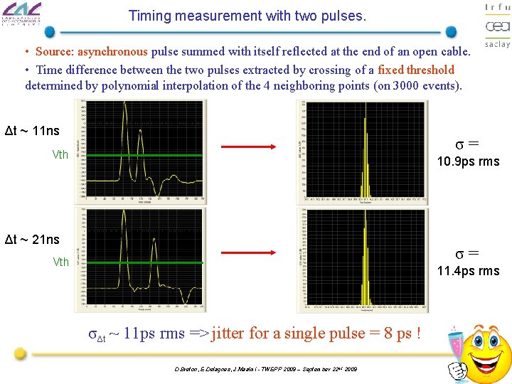
Timing measurement with two pulses. • Source: asynchronous pulse summed with itself reflected at the end of an open cable. • Time difference between the two pulses extracted by crossing of a fixed threshold determined by polynomial interpolation of the 4 neighboring points (on 3000 events). Δt ~ 11 ns σ= Vth 10. 9 ps rms Δt ~ 21 ns σ= Vth 11. 4 ps rms σΔt ~ 11 ps rms => jitter for a single pulse = 8 ps ! D. Breton, E. Delagnes, J. Maalmi - TWEPP 2009 – September 22 nd 2009

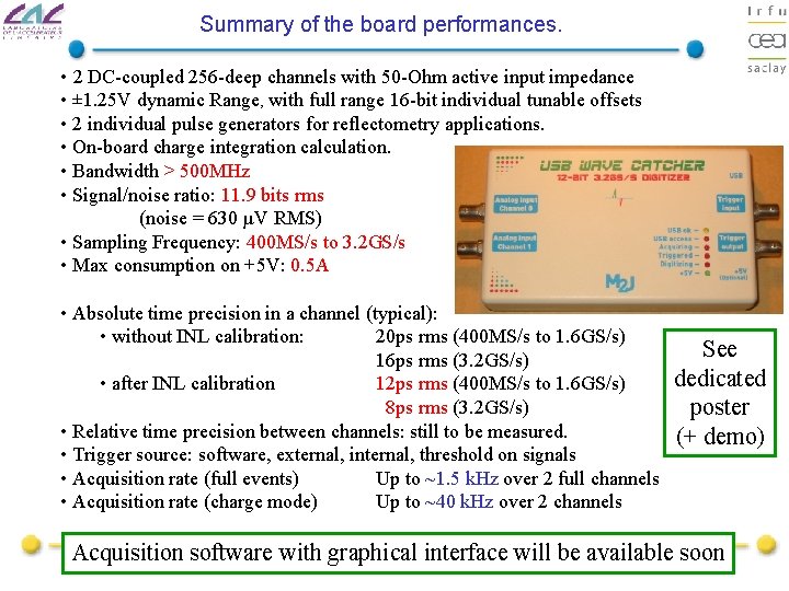
Summary of the board performances. • 2 DC-coupled 256 -deep channels with 50 -Ohm active input impedance • ± 1. 25 V dynamic Range, with full range 16 -bit individual tunable offsets • 2 individual pulse generators for reflectometry applications. • On-board charge integration calculation. • Bandwidth > 500 MHz • Signal/noise ratio: 11. 9 bits rms (noise = 630 µV RMS) • Sampling Frequency: 400 MS/s to 3. 2 GS/s • Max consumption on +5 V: 0. 5 A • Absolute time precision in a channel (typical): • without INL calibration: 20 ps rms (400 MS/s to 1. 6 GS/s) See 16 ps rms (3. 2 GS/s) dedicated • after INL calibration 12 ps rms (400 MS/s to 1. 6 GS/s) 8 ps rms (3. 2 GS/s) poster • Relative time precision between channels: still to be measured. (+ demo) • Trigger source: software, external, internal, threshold on signals • Acquisition rate (full events) Up to ~1. 5 k. Hz over 2 full channels • Acquisition rate (charge mode) Up to ~40 k. Hz over 2 channels Acquisition software with graphical interface will be available soon D. Breton, E. Delagnes, J. Maalmi - TWEPP 2009 – September 22 nd 2009

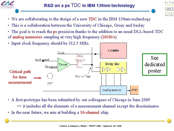
R&D on a ps TDC in IBM 130 nm technology • We are collaborating to the design of a new TDC in the IBM 130 nm technology • This is a collaboration between the University of Chicago, Orsay and Saclay • The goal is to reach the ps precision thanks to the addition to an usual DLL-based TDC of analog memories sampling at very high frequency (20 GS/s). • Input clock frequency should be 312. 5 MHz. See dedicated poster Critical path for time measurement • A first prototype has been submitted by our colleagues of Chicago in June 2009 => it includes all the elements of a measurement channel except the discriminator. • In the near future, we aim at building a 16 -channel chip. D. Breton, E. Delagnes, J. Maalmi - TWEPP 2009 – September 22 nd 2009

Conclusion • We built a USB board to push the SAM chip towards its limits. • Timing measurements showed a resolution of ~16 ps rms without time INL correction, and less than 10 ps after correction (SAM wasn’t even designed to this end !). • The board will soon be tested with MCPPMT’s for low-jitter light to time conversion. • The first boards of the last version are being cabled this week. • Tests showed us that analog memories look perfectly suited for ps time measurement. => no need for analog to digital pulse conversion, low power and low cost ! • This experience gave us new guidelines for future chips to improve timing performances. – We are now convinced that a single chip can’t be optimum for all applications (long depth vs time precision). – A new chip based on SAM was submitted last week to test higher bandwidth and lower power. – Next circuit will be submitted at the end of the year: 16 channels, 4 -5 GS/s sampling freq, larger BW (700 MHz ? ), larger depth (512 pts/ch), same techno (pure CMOS 0. 35µm), • A new 130 -nm pico-second TDC using ultra-fast analog memories is under design. D. Breton, E. Delagnes, J. Maalmi - TWEPP 2009 – September 22 nd 2009