Physics 124 Lecture 5 Binary Hexadecimal and Logic
Physics 124: Lecture 5 Binary, Hexadecimal, and Logic
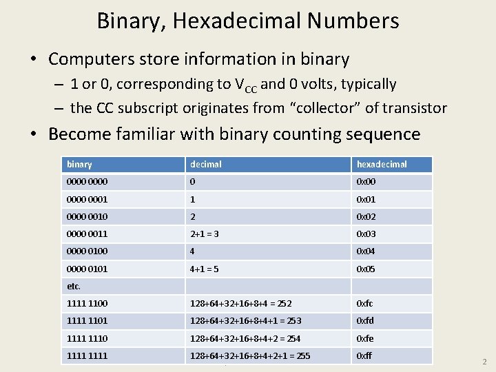
Binary, Hexadecimal Numbers • Computers store information in binary – 1 or 0, corresponding to VCC and 0 volts, typically – the CC subscript originates from “collector” of transistor • Become familiar with binary counting sequence binary decimal hexadecimal 0000 0 0 x 00 0001 1 0 x 01 0000 0010 2 0 x 02 0000 0011 2+1 = 3 0 x 03 0000 0100 4 0 x 04 0000 0101 4+1 = 5 0 x 05 1111 1100 128+64+32+16+8+4 = 252 0 xfc 1111 1101 128+64+32+16+8+4+1 = 253 0 xfd 1111 1110 128+64+32+16+8+4+2 = 254 0 xfe 1111 128+64+32+16+8+4+2+1 = 255 0 xff etc. Phys 124: Lecture 8 2
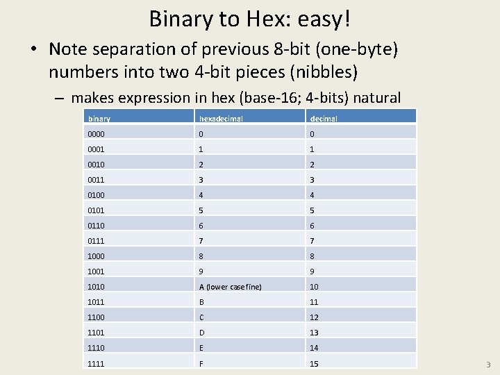
Binary to Hex: easy! • Note separation of previous 8 -bit (one-byte) numbers into two 4 -bit pieces (nibbles) – makes expression in hex (base-16; 4 -bits) natural binary hexadecimal 0000 0 0 0001 1 1 0010 2 2 0011 3 3 0100 4 4 0101 5 5 0110 6 6 0111 7 7 1000 8 8 1001 9 9 1010 A (lower case fine) 10 1011 B 11 1100 C 12 1101 D 13 1110 E 14 1111 F Phys 124: Lecture 8 15 3
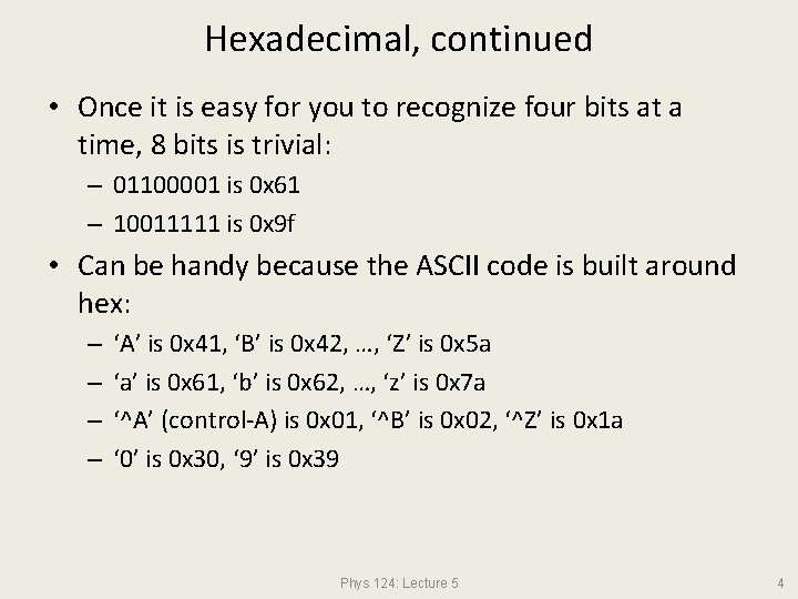
Hexadecimal, continued • Once it is easy for you to recognize four bits at a time, 8 bits is trivial: – 01100001 is 0 x 61 – 10011111 is 0 x 9 f • Can be handy because the ASCII code is built around hex: – – ‘A’ is 0 x 41, ‘B’ is 0 x 42, …, ‘Z’ is 0 x 5 a ‘a’ is 0 x 61, ‘b’ is 0 x 62, …, ‘z’ is 0 x 7 a ‘^A’ (control-A) is 0 x 01, ‘^B’ is 0 x 02, ‘^Z’ is 0 x 1 a ‘ 0’ is 0 x 30, ‘ 9’ is 0 x 39 Phys 124: Lecture 5 4

second hex digit ASCII Table in Hex 0 1 2 3 4 5 6 7 0 NUL ^@ null (�) DLE ^P SP space 0 @ P ` p 1 SOH ^A start of hdr DC 1 ^Q ! 1 A Q a q 2 STX ^B start text DC 2 ^R “ 2 B R b r 3 ETX ^C end text DC 3 ^S # 3 C S c s 4 EOT ^D end trans DC 4 ^T $ 4 D T d t 5 ENQ ^E NAK ^U % 5 E U e u 6 ACK ^F acknowledge SYN ^V & 6 F V f v 7 BEL ^G bell ETB ^W ‘ 7 G W g w 8 BS ^H backspace CAN ^X ( 8 H X h x 9 HT ^I horiz. tab (t) EM ^Y ) 9 I Y i y A LF ^J linefeed (r) SUB ^Z * : J Z j z B VT ^K vertical tab ESC escape + ; K [ k { C FF ^L form feed FS , < L l | D CR ^M carriage ret (n) GS - = M ] m } E SO ^N RS . > N ^ n ~ F SI ^O USPhys 124: Lecture 8 / ? O _ o DEL first hex digit 5
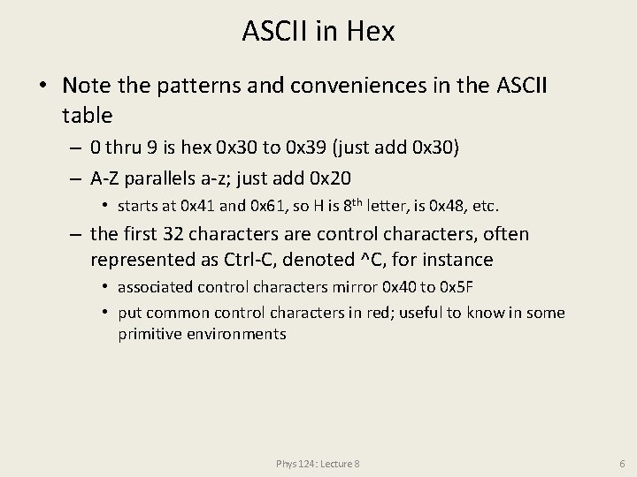
ASCII in Hex • Note the patterns and conveniences in the ASCII table – 0 thru 9 is hex 0 x 30 to 0 x 39 (just add 0 x 30) – A-Z parallels a-z; just add 0 x 20 • starts at 0 x 41 and 0 x 61, so H is 8 th letter, is 0 x 48, etc. – the first 32 characters are control characters, often represented as Ctrl-C, denoted ^C, for instance • associated control characters mirror 0 x 40 to 0 x 5 F • put common control characters in red; useful to know in some primitive environments Phys 124: Lecture 8 6
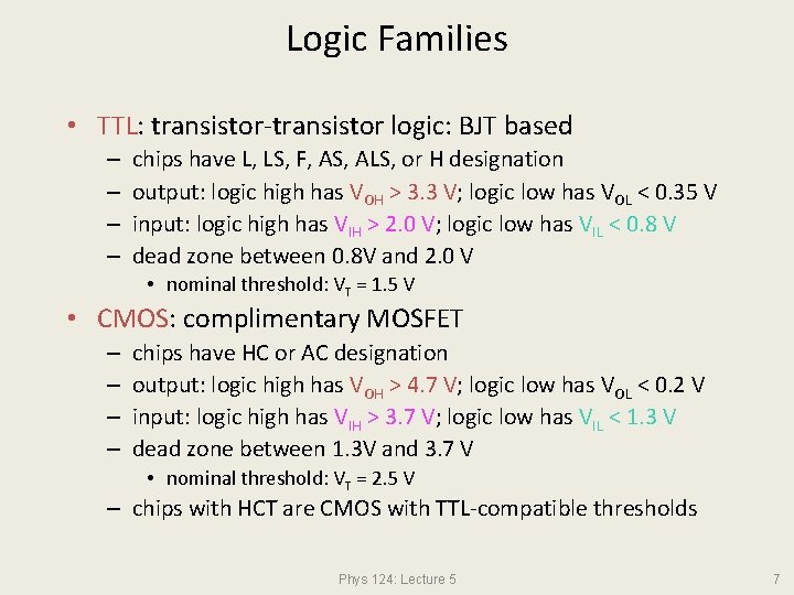
Logic Families • TTL: transistor-transistor logic: BJT based – – chips have L, LS, F, AS, ALS, or H designation output: logic high has VOH > 3. 3 V; logic low has VOL < 0. 35 V input: logic high has VIH > 2. 0 V; logic low has VIL < 0. 8 V dead zone between 0. 8 V and 2. 0 V • nominal threshold: VT = 1. 5 V • CMOS: complimentary MOSFET – – chips have HC or AC designation output: logic high has VOH > 4. 7 V; logic low has VOL < 0. 2 V input: logic high has VIH > 3. 7 V; logic low has VIL < 1. 3 V dead zone between 1. 3 V and 3. 7 V • nominal threshold: VT = 2. 5 V – chips with HCT are CMOS with TTL-compatible thresholds Phys 124: Lecture 5 7

Logic Family Levels • CMOS is closer to the “ideal” that logic low is zero volts and logic high is 5 volts – and has a bigger dead zone • The ? CT line accommodates both the TTL/CMOS levels • Example: A TTL device must: – interpret any input below 0. 8 V as logic low – interpret any input above 2. 0 V as logic high – put out at least 3. 3 V for logic high – put out less than 0. 35 V for logic low • The differing input/output thresholds lead to noise immunity Phys 124: Lecture 5 8
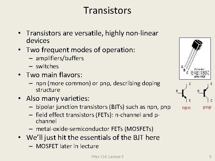
Transistors • Transistors are versatile, highly non-linear devices • Two frequent modes of operation: – amplifiers/buffers – switches • Two main flavors: – npn (more common) or pnp, describing doping structure • Also many varieties: – bipolar junction transistors (BJTs) such as npn, pnp – field effect transistors (FETs): n-channel and pchannel – metal-oxide-semiconductor FETs (MOSFETs) C B E C npn pnp • We’ll just hit the essentials of the BJT here – MOSFET later in lecture Phys 124: Lecture 5 9
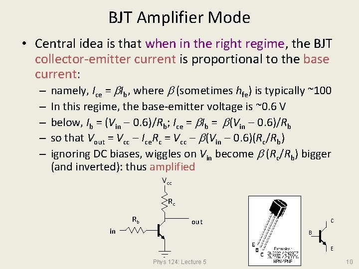
BJT Amplifier Mode • Central idea is that when in the right regime, the BJT collector-emitter current is proportional to the base current: – – – namely, Ice = Ib, where (sometimes hfe) is typically ~100 In this regime, the base-emitter voltage is ~0. 6 V below, Ib = (Vin 0. 6)/Rb; Ice = Ib = (Vin 0. 6)/Rb so that Vout = Vcc Ice. Rc = Vcc (Vin 0. 6)(Rc/Rb) ignoring DC biases, wiggles on Vin become (Rc/Rb) bigger (and inverted): thus amplified Vcc Rc Rb in out C B E Phys 124: Lecture 5 10
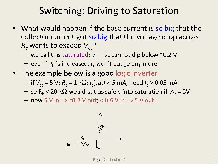
Switching: Driving to Saturation • What would happen if the base current is so big that the collector current got so big that the voltage drop across Rc wants to exceed Vcc? – we call this saturated: Vc Ve cannot dip below ~0. 2 V – even if Ib is increased, Ic won’t budge any more • The example below is a good logic inverter – if Vcc = 5 V; Rc = 1 k ; Ic(sat) 5 m. A; need Ib > 0. 05 m. A – so Rb < 20 k would put us safely into saturation if Vin = 5 V – now 5 V in ~0. 2 V out; < 0. 6 V in 5 V out Vcc Rc Rb in out Phys 124: Lecture 5 11
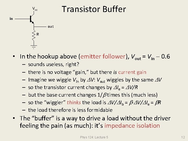
Transistor Buffer Vcc in out R • In the hookup above (emitter follower), Vout = Vin 0. 6 – – – – sounds useless, right? there is no voltage “gain, ” but there is current gain Imagine we wiggle Vin by V: Vout wiggles by the same V so the transistor current changes by Ie = V/R but the base current changes 1/ times this (much less) so the “wiggler” thinks the load is V/ Ib = · V/ Ie = R the load therefore is less formidable • The “buffer” is a way to drive a load without the driver feeling the pain (as much): it’s impedance isolation Phys 124: Lecture 5 12
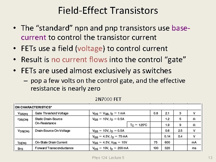
Field-Effect Transistors • The “standard” npn and pnp transistors use basecurrent to control the transistor current • FETs use a field (voltage) to control current • Result is no current flows into the control “gate” • FETs are used almost exclusively as switches – pop a few volts on the control gate, and the effective resistance is nearly zero 2 N 7000 FET Phys 124: Lecture 5 13
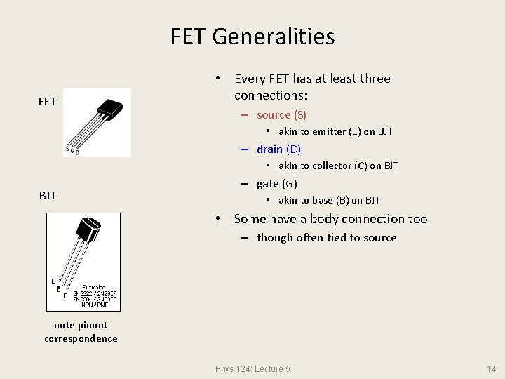
FET Generalities FET • Every FET has at least three connections: – source (S) • akin to emitter (E) on BJT – drain (D) • akin to collector (C) on BJT – gate (G) • akin to base (B) on BJT • Some have a body connection too – though often tied to source note pinout correspondence Phys 124: Lecture 5 14
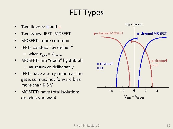
FET Types • • log current Two flavors: n and p Two types: JFET, MOSFETs more common JFETs conduct “by default” p-channel MOSFET n-channel MOSFET – when Vgate = Vsource • MOSFETs are “open” by default – must turn on deliberately p-channel JFET n-channel JFET • JFETs have a p-n junction at the gate, so must not forward bias more than 0. 6 V • MOSFETs have total isolation: do what you want Phys 124: Lecture 5 4 0 2 2 Vgate Vsource 4 15
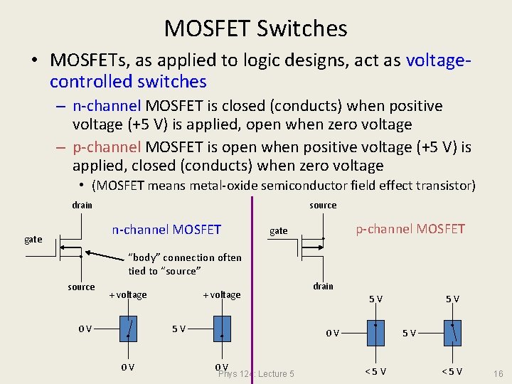
MOSFET Switches • MOSFETs, as applied to logic designs, act as voltagecontrolled switches – n-channel MOSFET is closed (conducts) when positive voltage (+5 V) is applied, open when zero voltage – p-channel MOSFET is open when positive voltage (+5 V) is applied, closed (conducts) when zero voltage • (MOSFET means metal-oxide semiconductor field effect transistor) drain source n-channel MOSFET gate p-channel MOSFET gate “body” connection often tied to “source” source + voltage 0 V + voltage 5 V 0 V drain 5 V 0 V 0 V Phys 124: Lecture 5 5 V 5 V <5 V 16
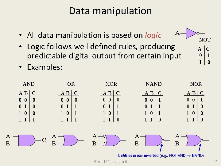
Data manipulation A • All data manipulation is based on logic • Logic follows well defined rules, producing predictable digital output from certain input • Examples: AND AB 0 0 0 1 1 A B OR C 0 0 0 1 AB 0 0 0 1 1 C A B XOR AB 0 0 0 1 1 C 0 1 1 1 NAND C 0 1 1 0 A B AB 0 0 0 1 1 A B NOT A C 0 1 1 0 NOR AB 0 0 0 1 1 C 1 1 1 0 C 1 0 0 0 A B bubbles mean inverted (e. g. , NOT AND NAND) Phys 124: Lecture 5 17
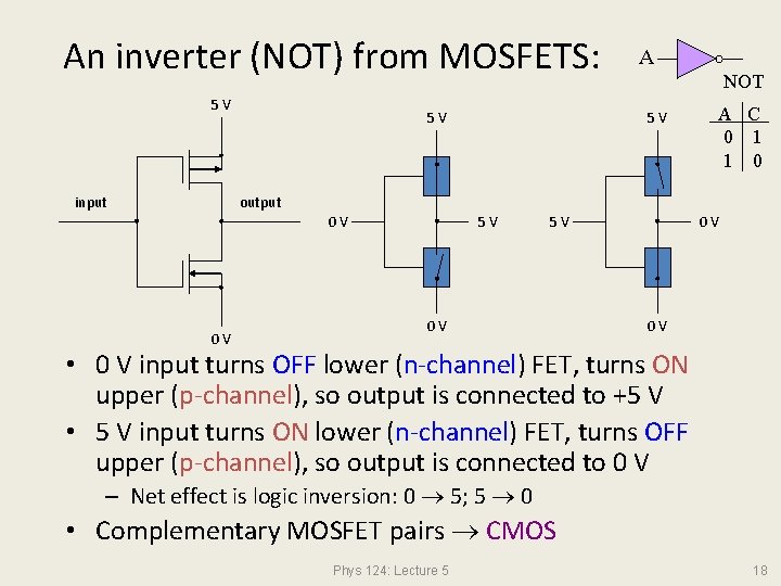
An inverter (NOT) from MOSFETS: 5 V input 5 V A NOT 5 V A C 0 1 1 0 output 0 V 0 V 5 V 5 V 0 V 0 V 0 V • 0 V input turns OFF lower (n-channel) FET, turns ON upper (p-channel), so output is connected to +5 V • 5 V input turns ON lower (n-channel) FET, turns OFF upper (p-channel), so output is connected to 0 V – Net effect is logic inversion: 0 5; 5 0 • Complementary MOSFET pairs CMOS Phys 124: Lecture 5 18
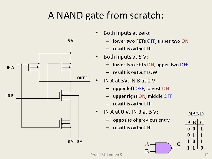
A NAND gate from scratch: • Both inputs at zero: – lower two FETs OFF, upper two ON – result is output HI 5 V • Both inputs at 5 V: IN A OUT C – lower two FETs ON, upper two OFF – result is output LOW • IN A at 5 V, IN B at 0 V: – upper left OFF, lowest ON – upper right ON, middle OFF – result is output HI IN B • IN A at 0 V, IN B at 5 V: NAND – opposite of previous entry – result is output HI 0 V 0 V Phys 124: Lecture 5 A B C AB 0 0 0 1 1 C 1 1 1 0 19
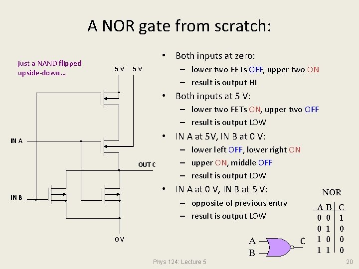
A NOR gate from scratch: just a NAND flipped upside-down… • Both inputs at zero: 5 V – lower two FETs OFF, upper two ON – result is output HI 5 V • Both inputs at 5 V: – lower two FETs ON, upper two OFF – result is output LOW • IN A at 5 V, IN B at 0 V: IN A OUT C – lower left OFF, lower right ON – upper ON, middle OFF – result is output LOW • IN A at 0 V, IN B at 5 V: IN B NOR – opposite of previous entry – result is output LOW 0 V A B Phys 124: Lecture 5 C AB 0 0 0 1 1 C 1 0 0 0 20
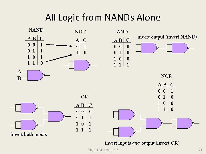
All Logic from NANDs Alone NAND NOT AB 0 0 0 1 1 A C 0 1 1 0 C 1 1 1 0 AND AB 0 0 0 1 1 A B invert output (invert NAND) NOR AB 0 0 0 1 1 OR invert both inputs C 0 0 0 1 AB 0 0 0 1 1 C 0 1 1 1 C 1 0 0 0 invert inputs and output (invert OR) Phys 124: Lecture 5 21
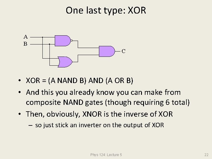
One last type: XOR A B C • XOR = (A NAND B) AND (A OR B) • And this you already know you can make from composite NAND gates (though requiring 6 total) • Then, obviously, XNOR is the inverse of XOR – so just stick an inverter on the output of XOR Phys 124: Lecture 5 22
Rule the World • Now you know how to build ALL logic gates out of n -channel and p-channel MOSFETs – because you can build a NAND from 4 MOSFETs – and all gates from NANDs • That means you can build computers • So now you can rule the world! Phys 124: Lecture 5 23
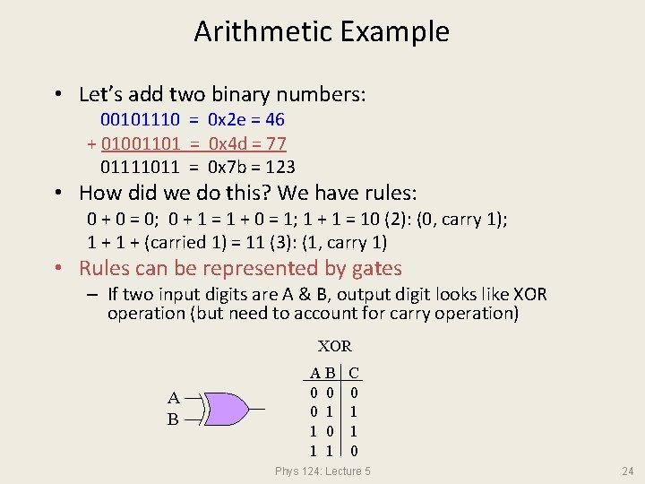
Arithmetic Example • Let’s add two binary numbers: 00101110 = 0 x 2 e = 46 + 01001101 = 0 x 4 d = 77 01111011 = 0 x 7 b = 123 • How did we do this? We have rules: 0 + 0 = 0; 0 + 1 = 1 + 0 = 1; 1 + 1 = 10 (2): (0, carry 1); 1 + (carried 1) = 11 (3): (1, carry 1) • Rules can be represented by gates – If two input digits are A & B, output digit looks like XOR operation (but need to account for carry operation) XOR A B AB 0 0 0 1 1 C 0 1 1 0 Phys 124: Lecture 5 24
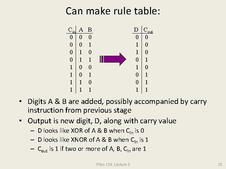
Can make rule table: Cin 0 0 1 1 A 0 0 1 1 B 0 1 0 1 D Cout 0 0 1 1 0 0 1 1 1 • Digits A & B are added, possibly accompanied by carry instruction from previous stage • Output is new digit, D, along with carry value – D looks like XOR of A & B when Cin is 0 – D looks like XNOR of A & B when Cin is 1 – Cout is 1 if two or more of A, B, Cin are 1 Phys 124: Lecture 5 25
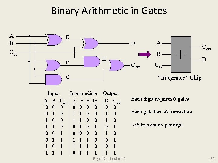
Binary Arithmetic in Gates A B Cin E D H F G A B Cout Cin + Cout D “Integrated” Chip Input Intermediate A B Cin E F H G 0 0 0 0 1 0 1 1 0 0 1 0 0 0 1 1 1 0 1 1 1 Output D Cout 0 0 1 1 0 0 1 1 1 Phys 124: Lecture 5 Each digit requires 6 gates Each gate has ~6 transistors ~36 transistors per digit 26
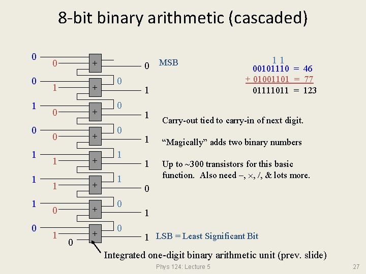
8 -bit binary arithmetic (cascaded) 0 0 1 1 1 0 0 + 1 + 0 + 1 + 0 0 MSB 0 0 0 1 1 11 00101110 = 46 + 01001101 = 77 01111011 = 123 Carry-out tied to carry-in of next digit. 1 “Magically” adds two binary numbers 1 Up to ~300 transistors for this basic function. Also need –, , , & lots more. 0 1 1 LSB = Least Significant Bit Integrated one-digit binary arithmetic unit (prev. slide) Phys 124: Lecture 5 27
Computer technology built up from pieces • The foregoing example illustrates the way in which computer technology is built – – – start with little pieces (transistors acting as switches) combine pieces into functional blocks (gates) combine these blocks into higher-level function (e. g. , addition) combine these new blocks into cascade (e. g. , 8 -bit addition) blocks get increasingly complex, more capable • Nobody on earth understands every nit of modern CPU – Grab previously developed blocks and run – Let a computer design the gate arrangements (eyes closed!) Phys 124: Lecture 5 28
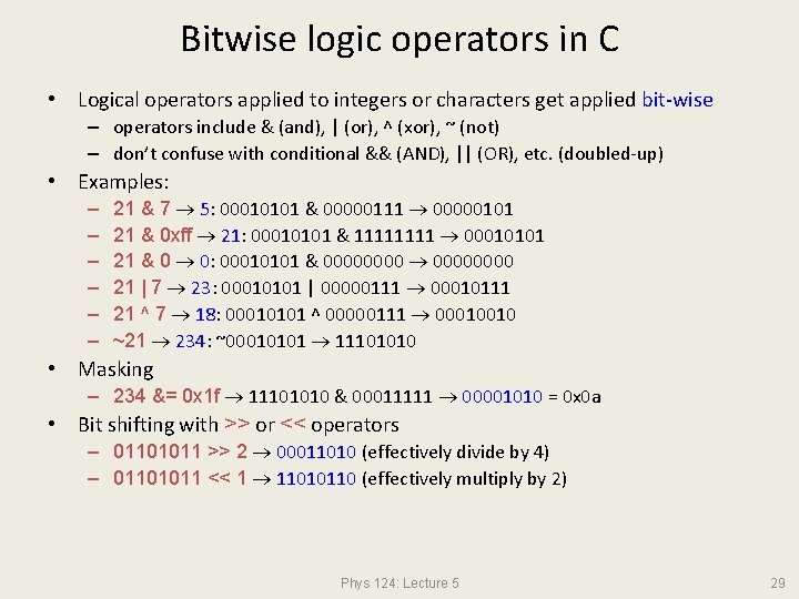
Bitwise logic operators in C • Logical operators applied to integers or characters get applied bit-wise – operators include & (and), | (or), ^ (xor), ~ (not) – don’t confuse with conditional && (AND), || (OR), etc. (doubled-up) • Examples: – – – 21 & 7 5: 00010101 & 00000111 00000101 21 & 0 xff 21: 00010101 & 1111 00010101 21 & 0 0: 00010101 & 00000000 21 | 7 23: 00010101 | 00000111 00010111 21 ^ 7 18: 00010101 ^ 00000111 00010010 ~21 234: ~00010101 11101010 • Masking – 234 &= 0 x 1 f 11101010 & 00011111 00001010 = 0 x 0 a • Bit shifting with >> or << operators – 01101011 >> 2 00011010 (effectively divide by 4) – 01101011 << 1 11010110 (effectively multiply by 2) Phys 124: Lecture 5 29
- Slides: 29