Physical Operation of BJTs Structure review Voltage vs
Physical Operation of BJTs • • Structure review Voltage vs. position in an npn structure – cutoff – active – saturation • Designing for high • The Early effect • Parasitic capacitance (Cp, Cm) From Prof. J. Hopwood

The npn Bipolar Junction Transistor n-type p-type n+-type collector emitter base E npn structure B integrated circuit BJT C metal silicon oxide doped silicon wafer (chip)
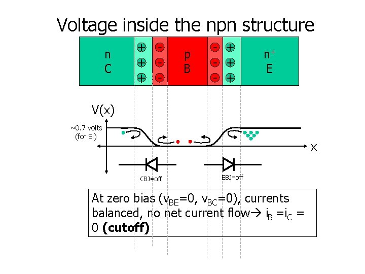
Voltage inside the npn structure n C + + + - p B - + - + n+ E V(x) ~0. 7 volts (for Si) x CBJ=off EBJ=off At zero bias (v. BE=0, v. BC=0), currents balanced, no net current flow i. B =i. C = 0 (cutoff)
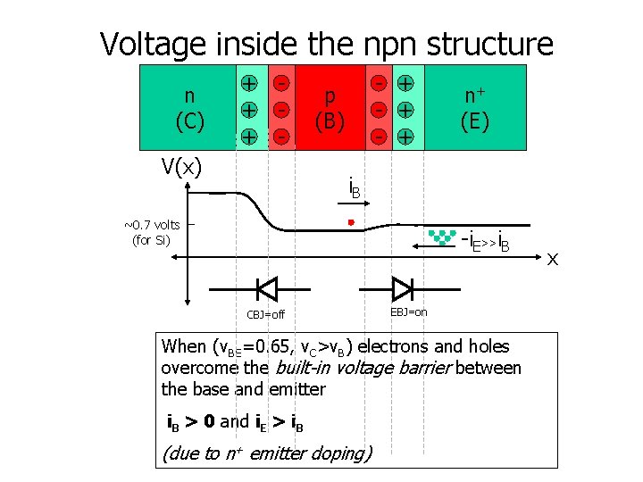
Voltage inside the npn structure n (C) + + + - V(x) - + - + p (B) n+ (E) i. B ~0. 7 volts (for Si) -i. E>>i. B CBJ=off EBJ=on When (v. BE=0. 65, v. C>v. B) electrons and holes overcome the built-in voltage barrier between the base and emitter i. B > 0 and i. E > i. B (due to n+ emitter doping) x
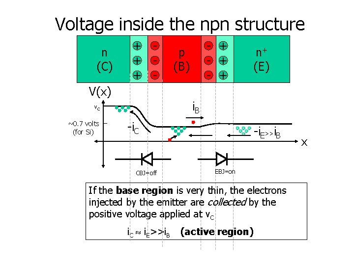
Voltage inside the npn structure n (C) + + + - - + - + p (B) n+ (E) V(x) i. B v. C ~0. 7 volts (for Si) -i. C CBJ=off -i. E>>i. B EBJ=on If the base region is very thin, the electrons injected by the emitter are collected by the positive voltage applied at v. C i. C i. E>>i. B (active region) x

Voltage inside the npn structure n (C) + + + - - + - + p (B) n+ (E) V(x) i. B v. C i. C ~0. 7 volts (for Si) i. E>>i. B CBJ=off x EBJ=on If the base region is too thick, the electrons injected by the emitter are lost by recombining with holes in the base before the voltage applied at v. C can collect them (another component of base current): i C < i. E (active region with low a, b)
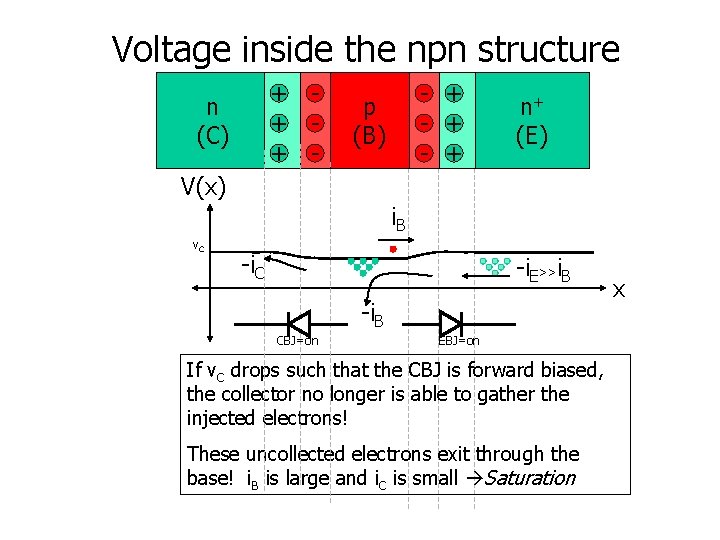
Voltage inside the npn structure + + + - n (C) - + - + p (B) n+ (E) V(x) i. B v. C -i. E>>i. B -i. B CBJ=on EBJ=on If v. C drops such that the CBJ is forward biased, the collector no longer is able to gather the injected electrons! These uncollected electrons exit through the base! i. B is large and i. C is small Saturation x
How do we achieve high ? • make the base region thin (typ. <1 micron) – this makes the collection efficiency of injected electrons high and decreases the chance of these electrons recombining in the base region • make the emitter heavily doped – i. E/i. B n(emitter)/p(base) (emitter doping concentration)/(base doping conc. ) These two quantities are difficult to control precisely! Therefore, the current gain is not uniform among BJTs (except when the BJTs are all made on the same chip. . . an integrated circuit)
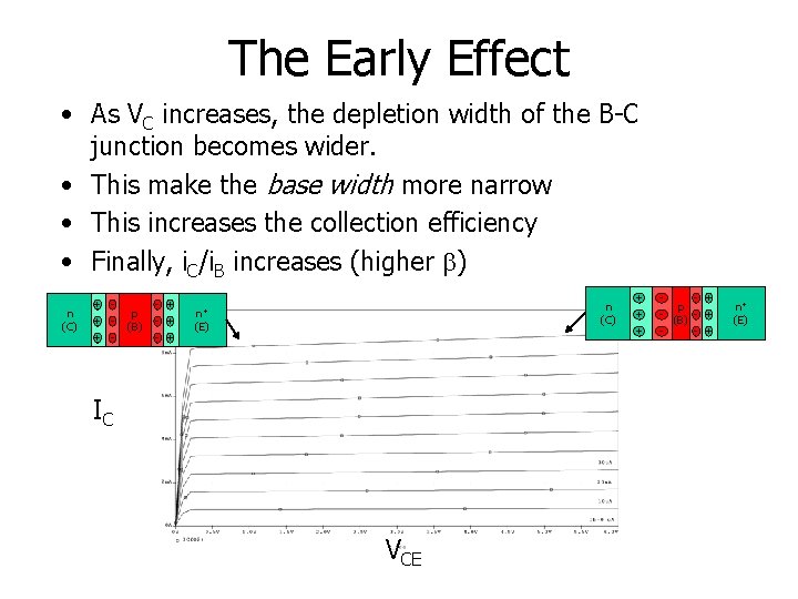
The Early Effect • As VC increases, the depletion width of the B-C junction becomes wider. • This make the base width more narrow • This increases the collection efficiency • Finally, i. C/i. B increases (higher ) n (C) + + + - p (B) - + - + n (C) n+ (E) IC VCE + + + - + p - (B) - + n+ (E)
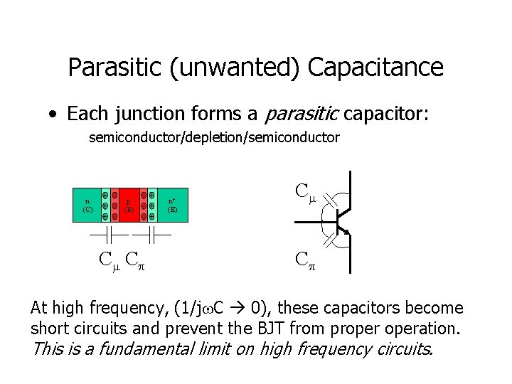
Parasitic (unwanted) Capacitance • Each junction forms a parasitic capacitor: semiconductor/depletion/semiconductor n (C) + + + - p (B) - + - + Cm Cp n+ (E) Cm Cp At high frequency, (1/jw. C 0), these capacitors become short circuits and prevent the BJT from properation. This is a fundamental limit on high frequency circuits.
- Slides: 10