
Physical Design and Fin FETs Rob Aitken ARM

Physical Design and Fin. FETs Rob Aitken ARM R&D San Jose, CA (with help from Greg Yeric, Brian Cline, Saurabh Sinha, Lucian Shifren, Imran Iqbal, Vikas Chandra and Dave Pietromonaco) 1
What’s Ahead? The Scaling Wall? EUV around the corner? Avalanches from resistance, variability, reliability, yield, etc. Slope of multiple patterning Crevasses of Doom Scaling getting rough Trade off area, speed, power, and (increasingly) cost 2
20 nm: End of the Line for Bulk § Barring something close to a miracle, 20 nm will be the last bulk node § § Conventional MOSFET limits have been reached Too much leakage for too little performance gain § Bulk replacement candidates § Short term: § § 3 Fin. FET/Tri-gate/Multi-gate, or FDSOI (maybe) Longer term (below 10 nm): § III-V devices, GAA, nanowires, etc. I come to fully deplete bulk, not to praise it
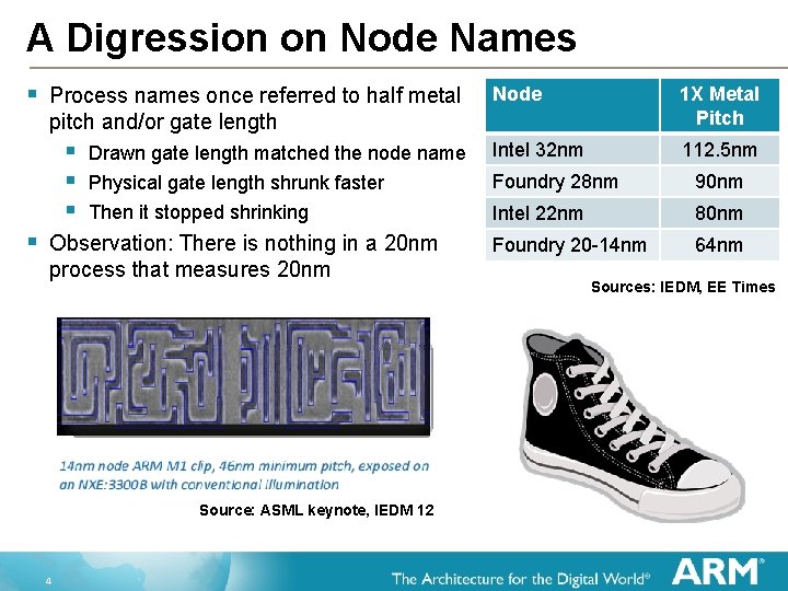
A Digression on Node Names § § § Node 1 X Metal Pitch Drawn gate length matched the node name Intel 32 nm 112. 5 nm Physical gate length shrunk faster Foundry 28 nm 90 nm Then it stopped shrinking Intel 22 nm 80 nm Foundry 20 -14 nm 64 nm Process names once referred to half metal pitch and/or gate length Observation: There is nothing in a 20 nm process that measures 20 nm Source: ASML keynote, IEDM 12 4 Sources: IEDM, EE Times
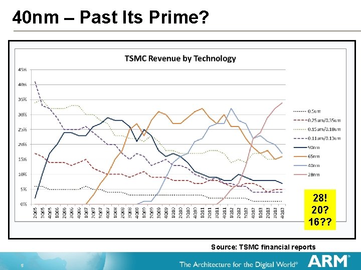
40 nm – Past Its Prime? 28! 20? 16? ? Source: TSMC financial reports 5

Technology Scaling Trends The Good Old Days Complexity Interconnect Lithography scaling Patterning Transistors PMOS Wires negligible HKMG Strain Strong RET LE, <l Planar CMOS NMOS LE, ~l CU wires Al wires 1970 6 1980 1990 2000 2010 2020
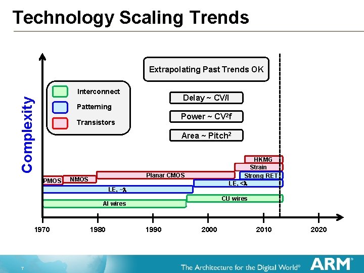
Technology Scaling Trends Extrapolating Past Trends OK Complexity Interconnect Delay ~ CV/I Patterning Power ~ CV 2 f Transistors Area ~ Pitch 2 PMOS HKMG Strain Strong RET LE, <l Planar CMOS NMOS LE, ~l CU wires Al wires 1970 7 1980 1990 2000 2010 2020
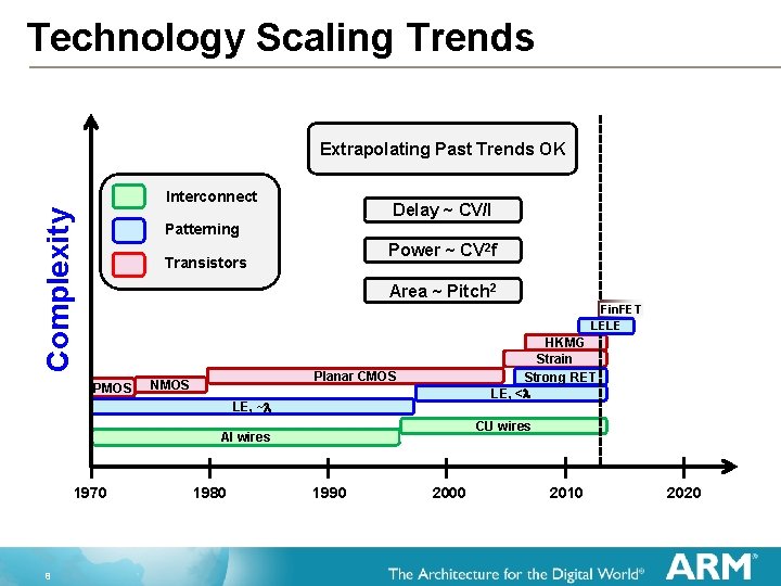
Technology Scaling Trends Extrapolating Past Trends OK Complexity Interconnect Delay ~ CV/I Patterning Power ~ CV 2 f Transistors Area ~ Pitch 2 Fin. FET LELE PMOS HKMG Strain Strong RET LE, <l Planar CMOS NMOS LE, ~l CU wires Al wires 1970 8 1980 1990 2000 2010 2020
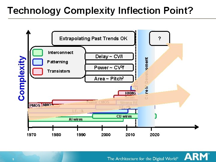
Technology Complexity Inflection Point? ? Complexity Interconnect Delay ~ CV/I Patterning Power ~ CV 2 f Transistors Area ~ Pitch 2 Fin. FET LELE Planar CMOS PMOS NMOS LE, ~l 1970 1980 1990 HKMG Strain Strong RET LE, <l CU wires Al wires 9 Core IP Development Extrapolating Past Trends OK 2000 2010 2020

Technology Complexity Inflection Point? Complexity Interconnect Patterning Transistors Fin. FET LELE Planar CMOS PMOS NMOS LE, ~l CU wires Al wires 1970 10 1980 1990 HKMG Strain Strong RET LE, <l 2000 2010 2020
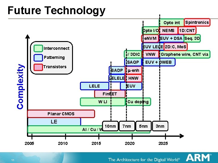
Future Technology Opto int Opto I/O NEMS Spintronics 1 D: CNT e. NVM EUV + DSA Seq. 3 D EUV LELE 2 D: C, Mo. S Interconnect Complexity Patterning Transistors SADP // 3 DIC VNW Graphene wire, CNT via SAQP EUV + DWEB m-enh LELELE HNW LELE EUV Fin. FET W LI Cu doping Planar CMOS LE 2005 11 10 nm Al / Cu / W wires 2010 2015 7 nm 2020 5 nm 3 nm 2025
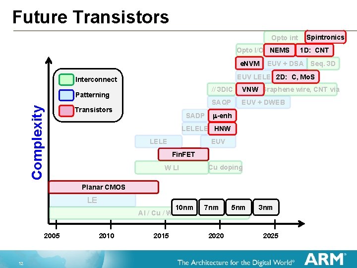
Future Transistors Opto int Opto I/O NEMS e. NVM Complexity Patterning EUV + DSA Seq. 3 D Transistors SADP // 3 DIC VNW Graphene wire, CNT via SAQP EUV + DWEB m-enh LELELE HNW LELE EUV Fin. FET W LI Cu doping Planar CMOS 2005 12 10 nm Al / Cu / W wires 2010 1 D: CNT EUV LELE 2 D: C, Mo. S Interconnect LE Spintronics 2015 7 nm 2020 5 nm 3 nm 2025
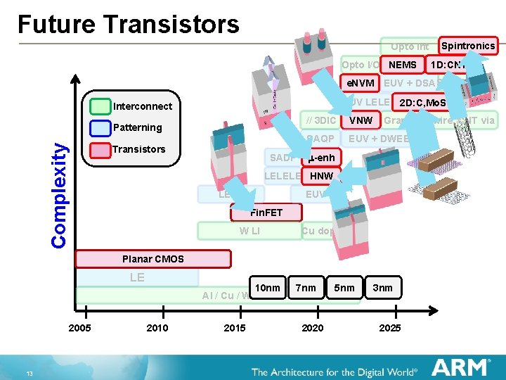
Future Transistors Opto int Opto I/O NEMS e. NVM Complexity Patterning EUV + DSA Seq. 3 D Transistors SADP // 3 DIC VNW Graphene wire, CNT via SAQP EUV + DWEB m-enh LELELE HNW LELE EUV Fin. FET W LI Cu doping Planar CMOS 2005 13 10 nm Al / Cu / W wires 2010 1 D: CNT EUV LELE 2 D: C, Mo. S Interconnect LE Spintronics 2015 7 nm 2020 5 nm 3 nm 2025
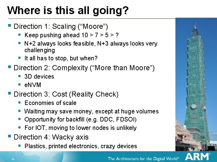
Where is this all going? § Direction 1: Scaling (“Moore”) § § § Keep pushing ahead 10 > 7 > 5 > ? N+2 always looks feasible, N+3 always looks very challenging It all has to stop, but when? § § 3 D devices e. NVM § § Economies of scale Waiting may save money, except at huge volumes Opportunity for backfill (e. g. DDC, FDSOI) For IOT, moving to lower nodes is unlikely § Plastics, printed electronics, crazy devices § Direction 2: Complexity (“More than Moore”) § Direction 3: Cost (Reality Check) § Direction 4: Wacky axis 14
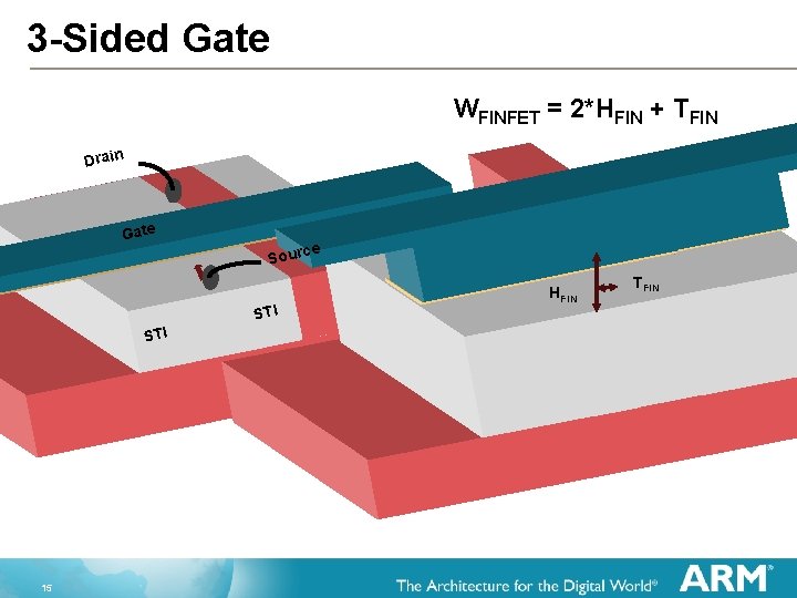
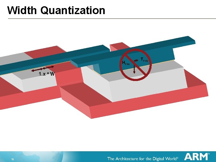
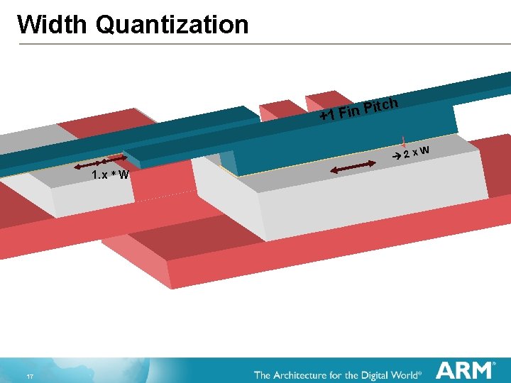
3 -Sided Gate WFINFET = 2*HFIN + TFIN Drain Gate e Sourc STI 15 HFIN TFIN
Width Quantization HFIN 1. x * W 16 TFIN
Width Quantization itch P n i F +1 2 x 1. x * W 17 W
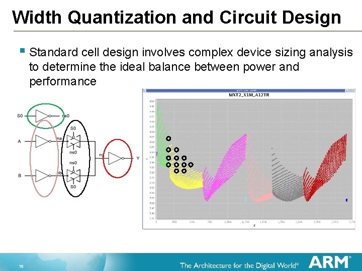
Width Quantization and Circuit Design § Standard cell design involves complex device sizing analysis to determine the ideal balance between power and performance 18
Fin Rules and Design Complexity 19

Allocating Active and Dummy Fins 20
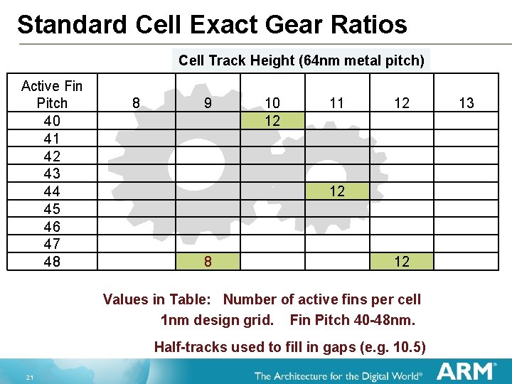
Standard Cell Exact Gear Ratios Cell Track Height (64 nm metal pitch) Active Fin Pitch 40 41 42 43 44 45 46 47 48 8 9 10 12 11 12 8 12 Values in Table: Number of active fins per cell 1 nm design grid. Fin Pitch 40 -48 nm. Half-tracks used to fill in gaps (e. g. 10. 5) 21 13
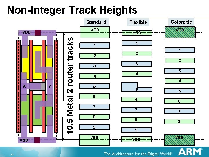
Non-Integer Track Heights Standard VDD A VSS 22 Y 10. 5 Metal 2 router tracks VDD 1 2 3 4 Flexible VDD Colorable VDD 1 2 3 4 5 6 7 8 9 VSS 5 5 6 6 7 7 8 8 9 VSS
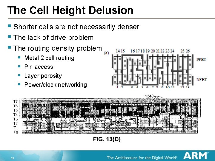
The Cell Height Delusion § Shorter cells are not necessarily denser § The lack of drive problem § The routing density problem § § 23 Metal 2 cell routing Pin access Layer porosity Power/clock networking
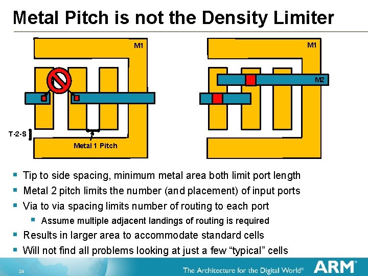
Metal Pitch is not the Density Limiter M 1 M 2 T-2 -S Metal 1 Pitch § § § Tip to side spacing, minimum metal area both limit port length Metal 2 pitch limits the number (and placement) of input ports Via to via spacing limits number of routing to each port § § § Assume multiple adjacent landings of routing is required Results in larger area to accommodate standard cells Will not find all problems looking at just a few “typical” cells 24
Pin Access is a Major Challenge 25
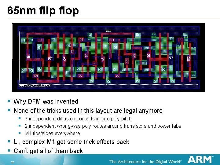
65 nm flip flop § § Why DFM was invented None of the tricks used in this layout are legal anymore § 3 independent diffusion contacts in one poly pitch § 2 independent wrong-way poly routes around transistors and power tabs § M 1 tips/sides everywhere LI, complex M 1 get some trick effects back Can’t get all of them back 26
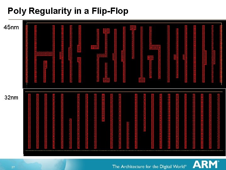
Poly Regularity in a Flip-Flop 45 nm <32 nm 27
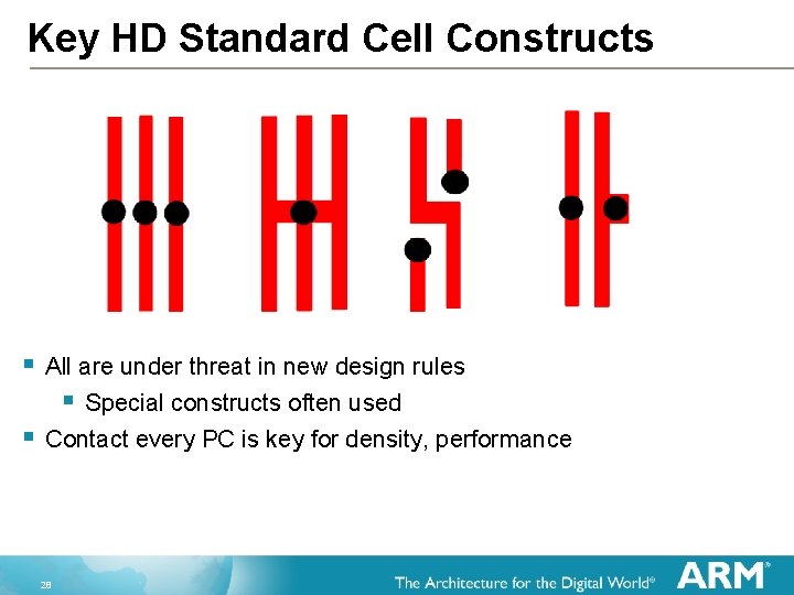
Key HD Standard Cell Constructs § All are under threat in new design rules § Special constructs often used § Contact every PC is key for density, performance 28
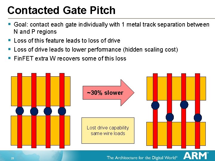
Contacted Gate Pitch § Goal: contact each gate individually with 1 metal track separation between N and P regions § § § Loss of this feature leads to loss of drive Loss of drive leads to lower performance (hidden scaling cost) Fin. FET extra W recovers some of this loss ~30% slower Lost drive capability same wire loads 29
Below 28 nm, Double Patterning is Here 30
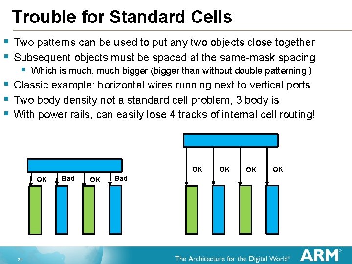
Trouble for Standard Cells § Two patterns can be used to put any two objects close together § Subsequent objects must be spaced at the same-mask spacing § Which is much, much bigger (bigger than without double patterning!) § Classic example: horizontal wires running next to vertical ports § Two body density not a standard cell problem, 3 body is § With power rails, can easily lose 4 tracks of internal cell routing! OK OK 31 Bad OK OK OK
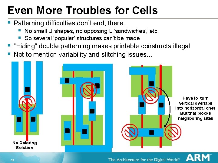
Even More Troubles for Cells § Patterning difficulties don’t end, there. § § No small U shapes, no opposing L ‘sandwiches’, etc. So several ‘popular’ structures can’t be made § “Hiding” double patterning makes printable constructs illegal § Not to mention variability and stitching issues… Have to turn vertical overlaps into horizontal ones But that blocks neighboring sites No Coloring Solution 32
Many Troubles, Any Hope? § Three body problem means peak wiring density cannot be achieved across a library § Standard cell and memory designers need to understand double patterning, even if it’s not explicitly in the rules § Decomposition and coloring tools are needed, whether simple or complex § LELE creates strong correlations in metal variability that all designers need to be aware of § With all of the above, it’s possible to get adequate density scaling going below 20 nm (barely) § Triple patterning, anyone? § What this means: Custom layout is extremely difficult. It will take longer than you expect! 33
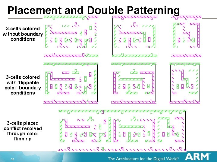
Placement and Double Patterning 3 -cells colored without boundary conditions 3 -cells colored with ‘flippable color’ boundary conditions 3 -cells placed conflict resolved through color flipping 34
Fin. FET Designer’s Cheat Sheet § Fewer Vt, L options § Slightly better leakage § New variation signatures § § Some local variation will reduce § Fin. FET 4 -input NAND ~ planar 3 -input NAND § x. OCV derates will need to reduce § Better tracking between device types § Reduced Inverted Temperature Dependence Little/no body effect § Paradigm shift in device strength per unit area § § 35 Get more done locally per clock cycle Watch the FET/wire balance (especially for hold) Expect better power gates Watch your power delivery network and electromigration!
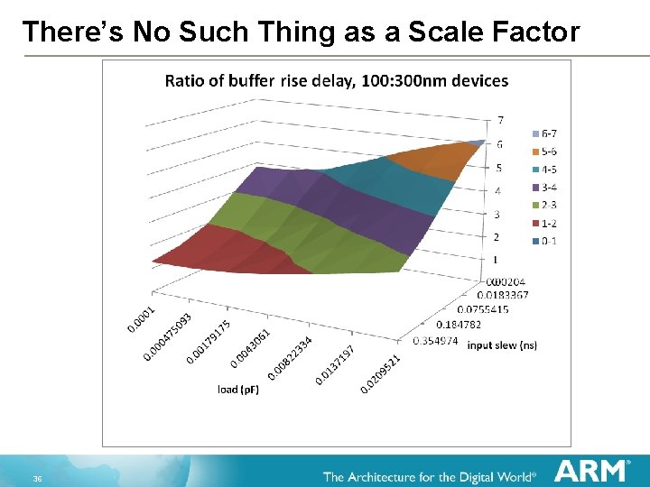
There’s No Such Thing as a Scale Factor 36
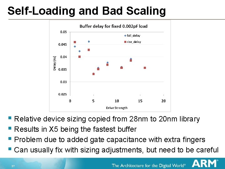
Self-Loading and Bad Scaling § Relative device sizing copied from 28 nm to 20 nm library § Results in X 5 being the fastest buffer § Problem due to added gate capacitance with extra fingers § Can usually fix with sizing adjustments, but need to be careful 37
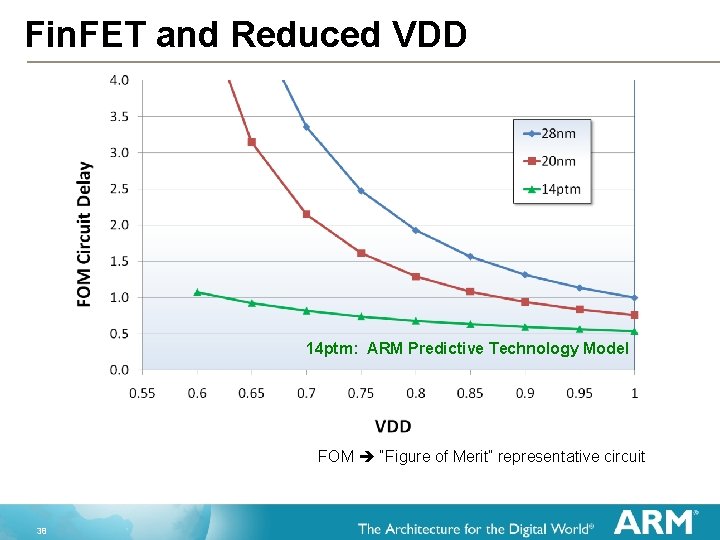
Fin. FET and Reduced VDD 14 ptm: ARM Predictive Technology Model FOM “Figure of Merit” representative circuit 38
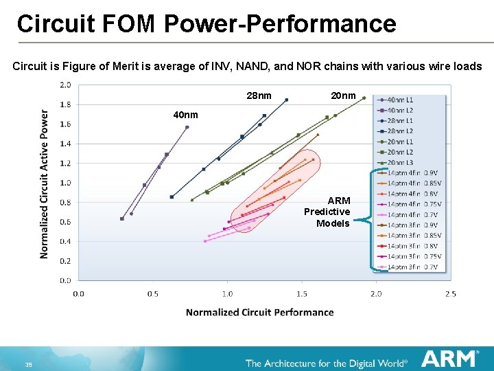
Circuit FOM Power-Performance Circuit is Figure of Merit is average of INV, NAND, and NOR chains with various wire loads 28 nm 20 nm 40 nm ARM Predictive Models 39
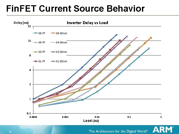
Fin. FET Current Source Behavior Inverter Delay vs Load Delay (au) 32 16 8 X 8 -FF X 8 -28 nm X 4 -FF X 4 -28 nm X 2 -FF X 2 -28 nm X 1 -FF X 1 -28 nm 4 2 1 0. 5 0. 0001 0. 01 Load (au) 40 0. 1 1
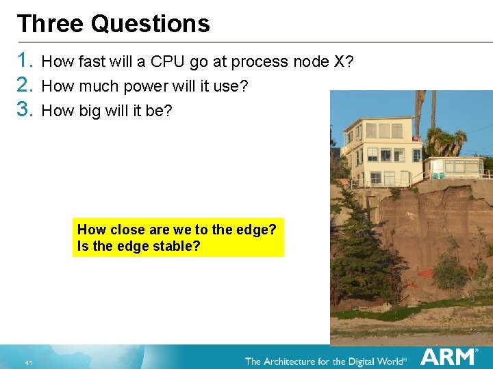
Three Questions 1. 2. 3. How fast will a CPU go at process node X? How much power will it use? How big will it be? How close are we to the edge? Is the edge stable? 41
The Answers 1. How fast will a CPU go at process node X? § 2. How much power will it use? § § 3. Dynamic power? Can scale capacitance, voltage reasonably well Leakage? More than we’d like, but somewhat predictable How big will it be? § 42 Simple device/NAND/NOR models overpredict This one is easiest. Just need to guess layout rules, pin access and placement density. How hard can that be?

ARM PDK – Development & Complexity Predictive PDK Electrical Models (BSIM CMG) Vth 43 s Temperature Dependence DRC LVS Lithography Dependence Fin. FET Parameter Handling Tech. LEF (LEFDEF Standard) Extraction (ITF Standard) Mask Layer Derivations Stack Composition R&C Matching Lithography Dependence
Predictive 10 nm Library § 2 basic litho options: SADP and LELELE § 2 fin options: 3 fin and 4 fin § 10 and 12 fin library height § Gives 4 combinations for library § § 54 cells 2 flops Max X 2 drive on non INV/BUF NAND, NOR plus ADD, AOI, OAI, PREICG, XOR, XNOR § Can be used as-is to synthesize simple designs 44
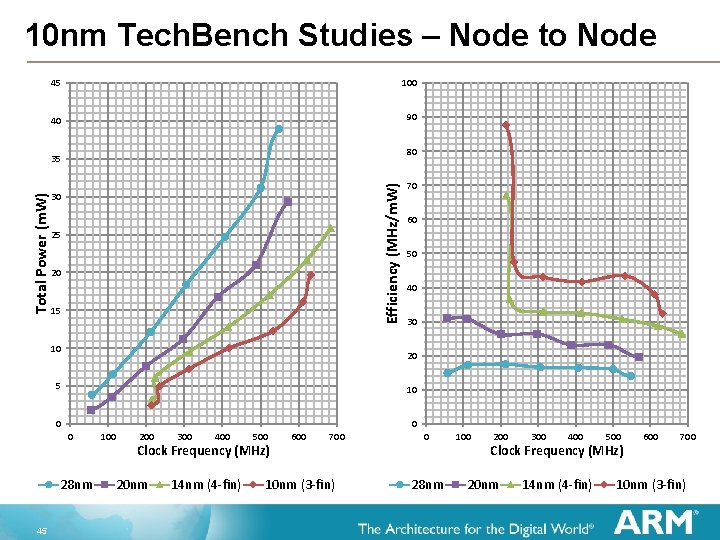
10 nm Tech. Bench Studies – Node to Node 45 100 40 90 80 Efficiency (MHz/m. W) Total Power (m. W) 35 30 25 20 15 10 60 50 40 30 20 5 10 0 28 nm 45 70 100 200 300 400 500 Clock Frequency (MHz) 20 nm 14 nm (4 -fin) 600 700 10 nm (3 -fin) 0 28 nm 100 200 300 400 500 Clock Frequency (MHz) 20 nm 14 nm (4 -fin) 600 700 10 nm (3 -fin)
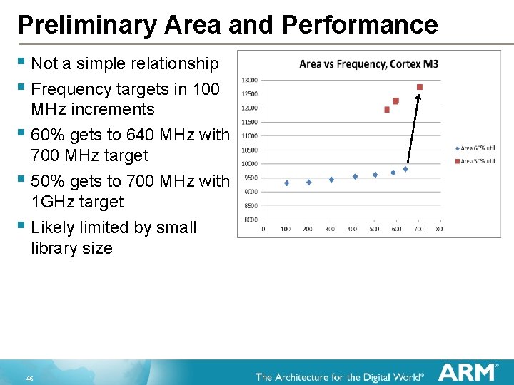
Preliminary Area and Performance § Not a simple relationship § Frequency targets in 100 MHz increments § 60% gets to 640 MHz with 700 MHz target § 50% gets to 700 MHz with 1 GHz target § Likely limited by small library size 46
What’s Ahead? § The original questions remain 1. 2. 3. How fast will a CPU go at process node X? How much power will it use? How big will it be? § New ones are added 4. 5. 6. 7. How should cores be allocated? How should they communicate? What’s the influence of software? What about X? (where X is EUV or DSA or III-V or Reliability or e. NVM or IOT or …. ) § Collaboration across companies, disciplines, ecosystems 47
Fin 48
- Slides: 48