
Phys 389 Semiconductor Applications L 8 1 Lecture


- Slides: 22
Phys 389 - Semiconductor Applications L 8 1 Lecture 8: Junctions with metals • Metals as interconnects – Electromigration • Schottky barrier Diodes • Ohmic contacts • Insulator-semiconductor junctions • Interconnect technology • Moore’s Law
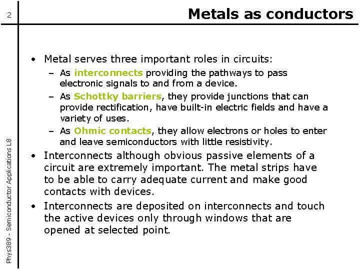
2 Metals as conductors Phys 389 - Semiconductor Applications L 8 • Metal serves three important roles in circuits: – As interconnects providing the pathways to pass electronic signals to and from a device. – As Schottky barriers, they provide junctions that can provide rectification, have built-in electric fields and have a variety of uses. – As Ohmic contacts, they allow electrons or holes to enter and leave semiconductors with little resistivity. • Interconnects although obvious passive elements of a circuit are extremely important. The metal strips have to be able to carry adequate current and make good contacts with devices. • Interconnects are deposited on interconnects and touch the active devices only through windows that are opened at selected point.
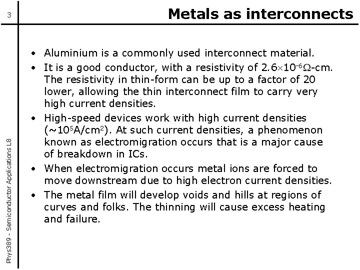
Phys 389 - Semiconductor Applications L 8 3 Metals as interconnects • Aluminium is a commonly used interconnect material. • It is a good conductor, with a resistivity of 2. 6 10 -6 W-cm. The resistivity in thin-form can be up to a factor of 20 lower, allowing the thin interconnect film to carry very high current densities. • High-speed devices work with high current densities (~105 A/cm 2). At such current densities, a phenomenon known as electromigration occurs that is a major cause of breakdown in ICs. • When electromigration occurs metal ions are forced to move downstream due to high electron current densities. • The metal film will develop voids and hills at regions of curves and folks. The thinning will cause excess heating and failure.
Phys 389 - Semiconductor Applications L 8 4 Electromigration • Electromigration occurs mainly along the grain structure. Prevention of this phenomenon requires that the grain structure is controlled along the microcrystallites that form the metal lines. • Larger grains have less surface area and therefore resist electromigration. • Some allowing metals, such as copper, accumulate in the grain boundaries, locking the atoms there into place and preventing electromigration. • Copper also prevents hillocking of Al films and thus prevents non-uniform thermal effects. • Since 1998 scientists have been able to make interconnects from copper – delays in devices have been improved.
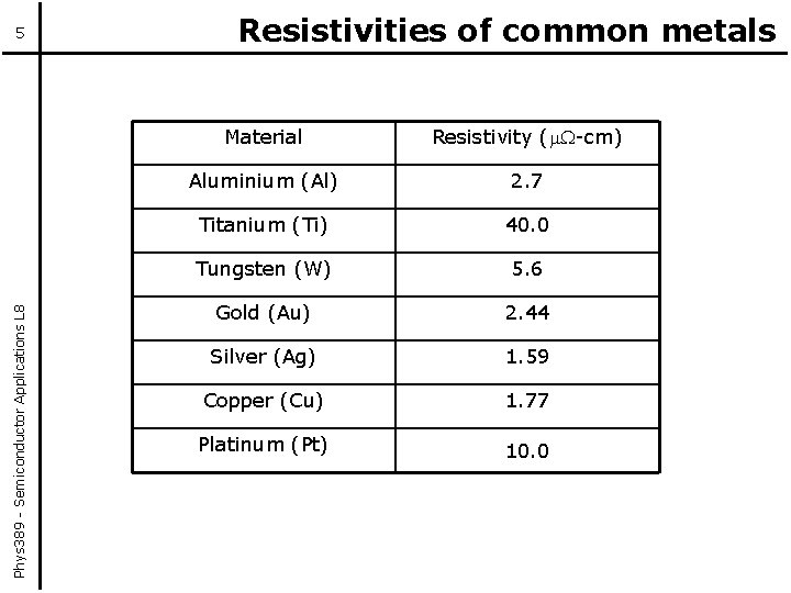
Phys 389 - Semiconductor Applications L 8 5 Resistivities of common metals Material Resistivity (m. W-cm) Aluminium (Al) 2. 7 Titanium (Ti) 40. 0 Tungsten (W) 5. 6 Gold (Au) 2. 44 Silver (Ag) 1. 59 Copper (Cu) 1. 77 Platinum (Pt) 10. 0
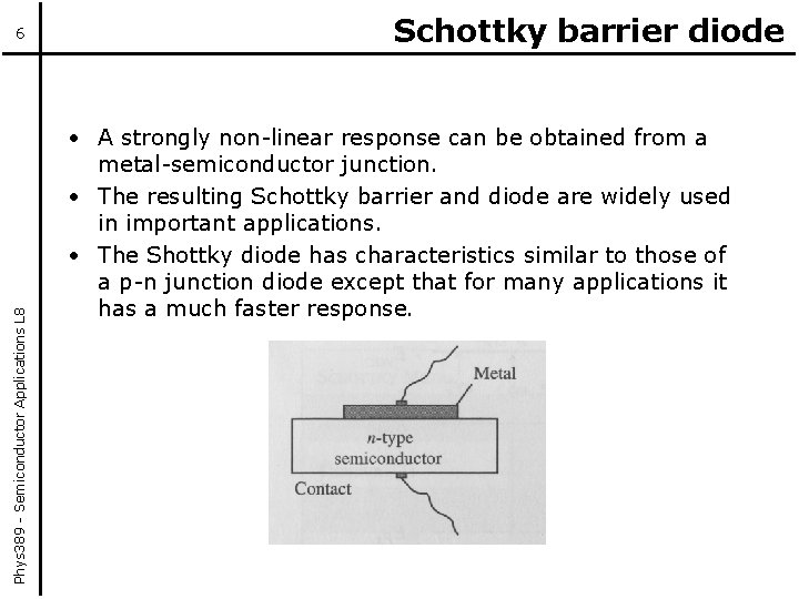
Phys 389 - Semiconductor Applications L 8 6 Schottky barrier diode • A strongly non-linear response can be obtained from a metal-semiconductor junction. • The resulting Schottky barrier and diode are widely used in important applications. • The Shottky diode has characteristics similar to those of a p-n junction diode except that for many applications it has a much faster response.
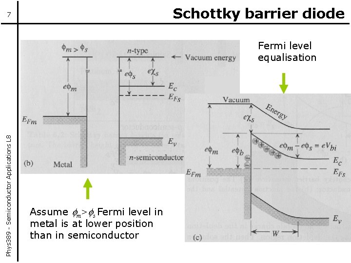
Schottky barrier diode 7 Phys 389 - Semiconductor Applications L 8 Fermi level equalisation Assume m> s Fermi level in metal is at lower position than in semiconductor
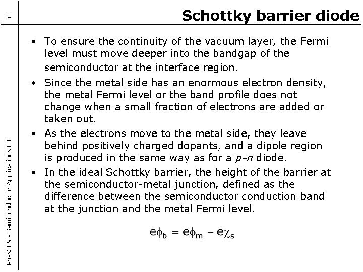
Phys 389 - Semiconductor Applications L 8 8 Schottky barrier diode • To ensure the continuity of the vacuum layer, the Fermi level must move deeper into the bandgap of the semiconductor at the interface region. • Since the metal side has an enormous electron density, the metal Fermi level or the band profile does not change when a small fraction of electrons are added or taken out. • As the electrons move to the metal side, they leave behind positively charged dopants, and a dipole region is produced in the same way as for a p-n diode. • In the ideal Schottky barrier, the height of the barrier at the semiconductor-metal junction, defined as the difference between the semiconductor conduction band at the junction and the metal Fermi level.
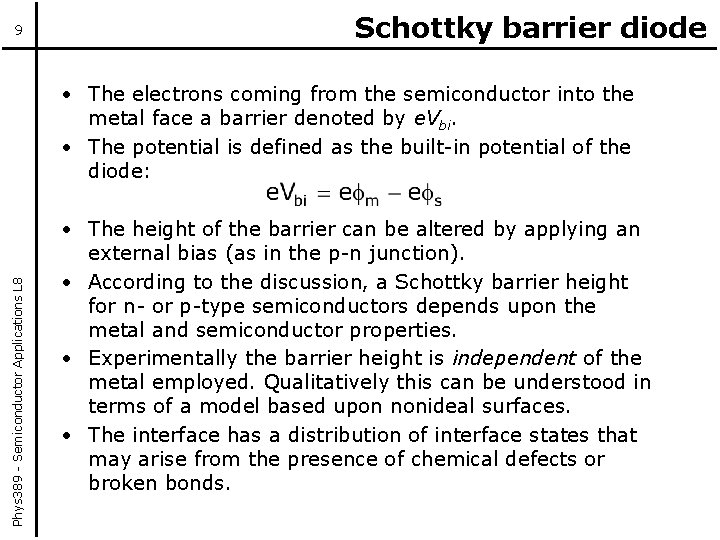
9 Schottky barrier diode Phys 389 - Semiconductor Applications L 8 • The electrons coming from the semiconductor into the metal face a barrier denoted by e. Vbi. • The potential is defined as the built-in potential of the diode: • The height of the barrier can be altered by applying an external bias (as in the p-n junction). • According to the discussion, a Schottky barrier height for n- or p-type semiconductors depends upon the metal and semiconductor properties. • Experimentally the barrier height is independent of the metal employed. Qualitatively this can be understood in terms of a model based upon nonideal surfaces. • The interface has a distribution of interface states that may arise from the presence of chemical defects or broken bonds.
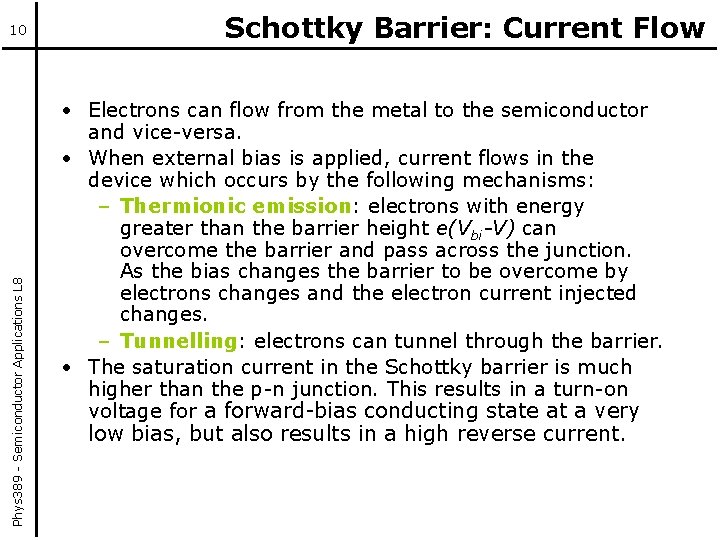
Phys 389 - Semiconductor Applications L 8 10 Schottky Barrier: Current Flow • Electrons can flow from the metal to the semiconductor and vice-versa. • When external bias is applied, current flows in the device which occurs by the following mechanisms: – Thermionic emission: electrons with energy greater than the barrier height e(Vbi-V) can overcome the barrier and pass across the junction. As the bias changes the barrier to be overcome by electrons changes and the electron current injected changes. – Tunnelling: electrons can tunnel through the barrier. • The saturation current in the Schottky barrier is much higher than the p-n junction. This results in a turn-on voltage for a forward-bias conducting state at a very low bias, but also results in a high reverse current.
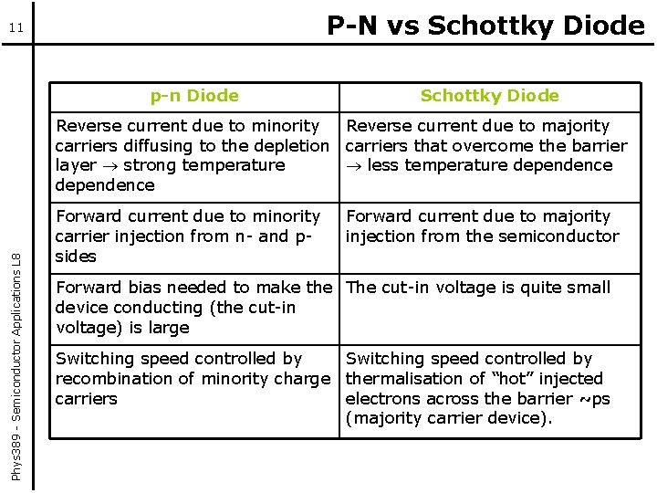
P-N vs Schottky Diode 11 p-n Diode Schottky Diode Phys 389 - Semiconductor Applications L 8 Reverse current due to minority Reverse current due to majority carriers diffusing to the depletion carriers that overcome the barrier layer strong temperature less temperature dependence Forward current due to minority carrier injection from n- and psides Forward current due to majority injection from the semiconductor Forward bias needed to make the The cut-in voltage is quite small device conducting (the cut-in voltage) is large Switching speed controlled by recombination of minority charge thermalisation of “hot” injected carriers electrons across the barrier ~ps (majority carrier device).
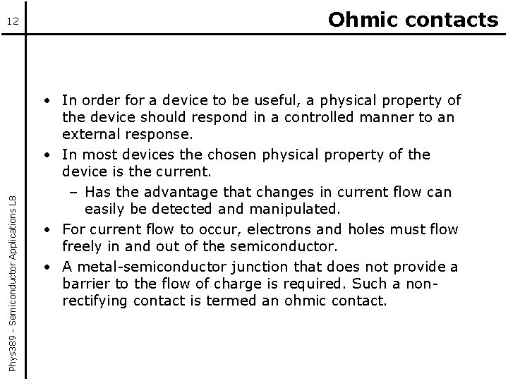
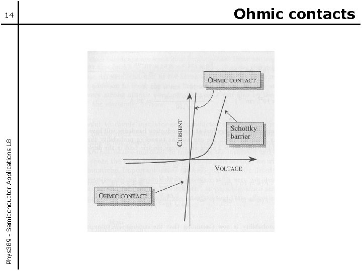
Phys 389 - Semiconductor Applications L 8 12 Ohmic contacts • In order for a device to be useful, a physical property of the device should respond in a controlled manner to an external response. • In most devices the chosen physical property of the device is the current. – Has the advantage that changes in current flow can easily be detected and manipulated. • For current flow to occur, electrons and holes must flow freely in and out of the semiconductor. • A metal-semiconductor junction that does not provide a barrier to the flow of charge is required. Such a nonrectifying contact is termed an ohmic contact.
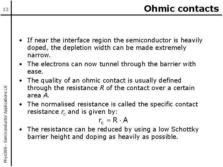
Phys 389 - Semiconductor Applications L 8 13 Ohmic contacts • If near the interface region the semiconductor is heavily doped, the depletion width can be made extremely narrow. • The electrons can now tunnel through the barrier with ease. • The quality of an ohmic contact is usually defined through the resistance R of the contact over a certain area A. • The normalised resistance is called the specific contact resistance rc and is given by: • The resistance can be reduced by using a low Schottky barrier height and doping as heavily as possible.
Phys 389 - Semiconductor Applications L 8 14 Ohmic contacts
Phys 389 - Semiconductor Applications L 8 15 Insulator-Semiconductor Junctions • There must be an isolation between an input and output signal of a device. • The silicon dioxide-silicon junction is the most important junction in solid state physics. – Despite the severe mismatch between Si. O 2 structure and Si structure, the interface quality is extremely high. – The ability to produce high quality interfaces is responsible for the remarkable success of metaloxide-silicon (MOS) devices. – Due to low interface densities, there is very little trapping of electrons (holes) at the interface so that high speed phenomena can be predictably used. – No other semiconductor has a natural oxide producing a high-quality interface give Si a unique advantage in electronic devices.
Phys 389 - Semiconductor Applications L 8 16 Interconnects • Presently the most important metal used for interconnects is aluminium and the most important insulator in microelectronics technology is Si. O 2. • Aluminium has a reasonably high conductivity and can be deposited without problems. • The key property of interconnects is the resistance associated with them and the maximum current density that can pass through without structural or electrical deterioration. • The ability of an interconnect to withstand high current densities (~105 A/cm 2) is an important requirement, since most microelectronic devices need high drive currents.
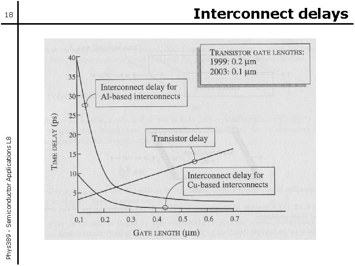
Phys 389 - Semiconductor Applications L 8 17 Interconnects • As the density of devices on a chip becomes higher, the area of a typical interconnect has to become smaller. • The RC delay time for signals to propagate from one device to another will increase. • Semiconductor Industry Associates estimate that interconnect delay will become increasingly dominant and overtake device-switching delay. • Copper (by virtue of its higher conductivity) is a material that has excellent potential. • Copper technology has finally matured and in 1998 made it into products for the first time. IBM began offering high performance processors based on copper technology.
Phys 389 - Semiconductor Applications L 8 18 Interconnect delays
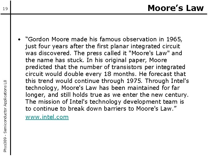
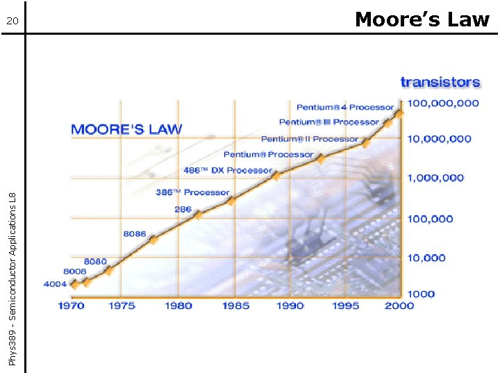
Phys 389 - Semiconductor Applications L 8 19 Moore’s Law • “Gordon Moore made his famous observation in 1965, just four years after the first planar integrated circuit was discovered. The press called it "Moore's Law" and the name has stuck. In his original paper, Moore predicted that the number of transistors per integrated circuit would double every 18 months. He forecast that this trend would continue through 1975. Through Intel's technology, Moore's Law has been maintained for far longer, and still holds true as we enter the new century. The mission of Intel's technology development team is to continue to break down barriers to Moore's Law. ” www. intel. com
Phys 389 - Semiconductor Applications L 8 20 Moore’s Law
Phys 389 - Semiconductor Applications L 8 21 Intel processor timeline
Phys 389 - Semiconductor Applications L 8 22 Summary of Lecture 8 • Metals as interconnects – Electromigration • Schottky barrier Diodes • Ohmic contacts • Insulator-semiconductor junctions • Interconnect technology • Moore’s Law