Photonic Sources Contents Review of Semiconductor Physics Light
![Internal Quantum Efficiency & Optical Power [4 -8] Optical power generated internally in the Internal Quantum Efficiency & Optical Power [4 -8] Optical power generated internally in the](https://slidetodoc.com/presentation_image/2a8ed2e40bb0b6bfacce34a97c5da9f4/image-21.jpg)
![External Quantum Eficiency [4 -10] • In order to calculate the external quantum efficiency, External Quantum Eficiency [4 -10] • In order to calculate the external quantum efficiency,](https://slidetodoc.com/presentation_image/2a8ed2e40bb0b6bfacce34a97c5da9f4/image-22.jpg)
![[4 -11] [4 -12] [4 -13] [4 -14] [4 -11] [4 -12] [4 -13] [4 -14]](https://slidetodoc.com/presentation_image/2a8ed2e40bb0b6bfacce34a97c5da9f4/image-23.jpg)
![[4 -17] Optical Fiber communications, 3 rd ed. , G. Keiser, Mc. Graw. Hill, [4 -17] Optical Fiber communications, 3 rd ed. , G. Keiser, Mc. Graw. Hill,](https://slidetodoc.com/presentation_image/2a8ed2e40bb0b6bfacce34a97c5da9f4/image-25.jpg)
- Slides: 25

Photonic Sources

Contents • Review of Semiconductor Physics • Light Emitting Diode (LED) - Structure, Material, Quantum efficiency, LED Power, Modulation • Laser Diodes - structure, Modes, Rate Equation, Quantum efficiency, Resonant frequencies, Radiation pattern • Single-Mode Lasers - DFB (Distributed-Feed. Back) laser, Distributed-Bragg Reflector, Modulation • Light-source Linearity • Noise in Lasers

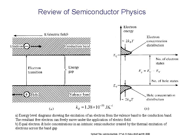
Review of Semiconductor Physics a) Energy level diagrams showing the excitation of an electron from the valence band to the conduction band. The resultant free electron can freely move under the application of electric field. b) Equal electron & hole concentrations in an intrinsic semiconductor created by thermal excitation of electrons across the band gap Optical Fiber communications, 3 rd ed. , G. Keiser, Mc. Graw. Hill, 2000

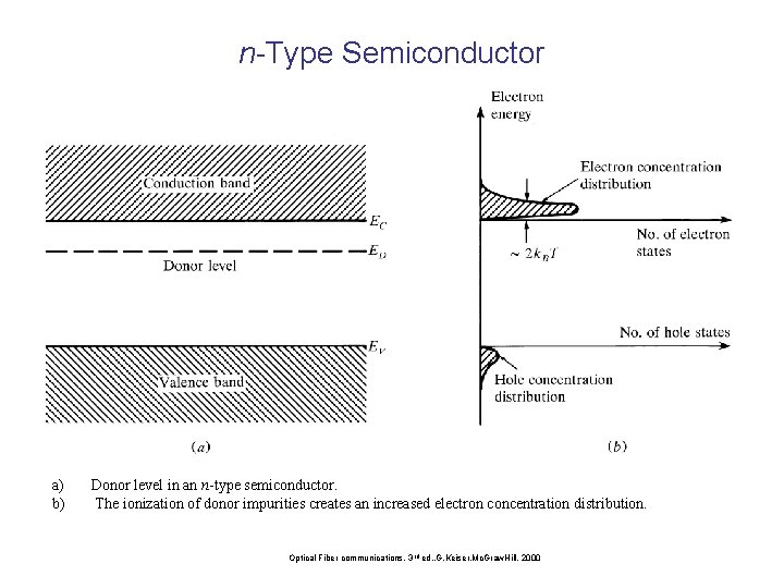
n-Type Semiconductor a) b) Donor level in an n-type semiconductor. The ionization of donor impurities creates an increased electron concentration distribution. Optical Fiber communications, 3 rd ed. , G. Keiser, Mc. Graw. Hill, 2000

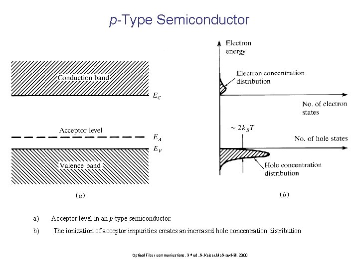
p-Type Semiconductor a) Acceptor level in an p-type semiconductor. b) The ionization of acceptor impurities creates an increased hole concentration distribution Optical Fiber communications, 3 rd ed. , G. Keiser, Mc. Graw. Hill, 2000

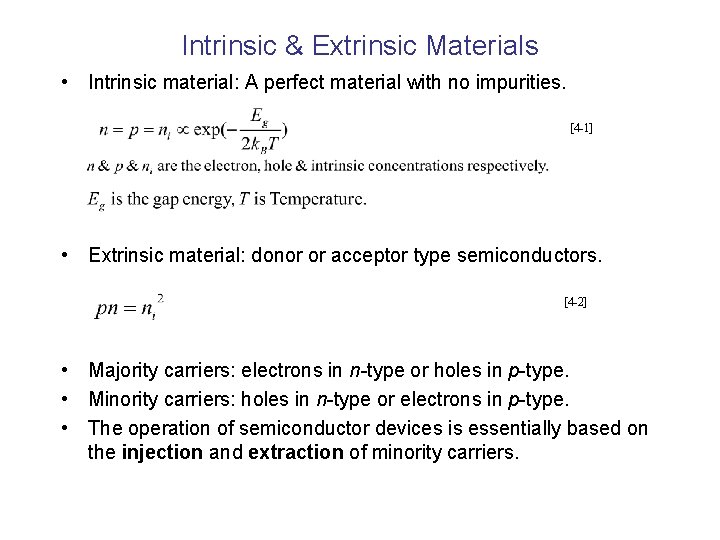
Intrinsic & Extrinsic Materials • Intrinsic material: A perfect material with no impurities. [4 -1] • Extrinsic material: donor or acceptor type semiconductors. [4 -2] • Majority carriers: electrons in n-type or holes in p-type. • Minority carriers: holes in n-type or electrons in p-type. • The operation of semiconductor devices is essentially based on the injection and extraction of minority carriers.

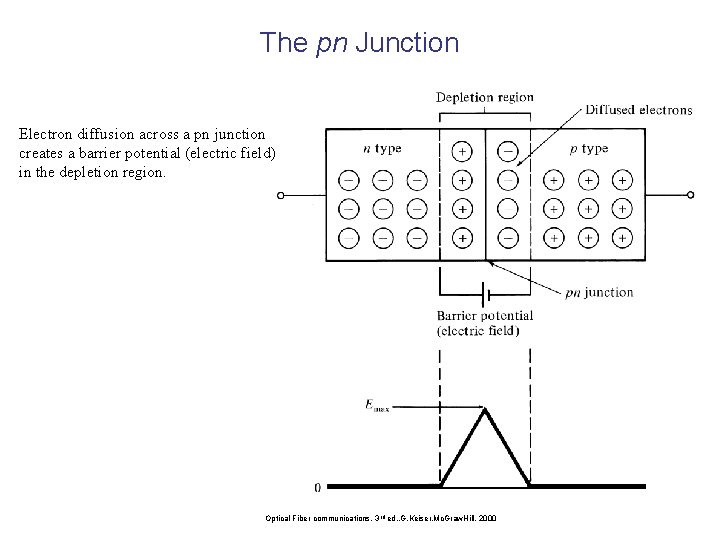
The pn Junction Electron diffusion across a pn junction creates a barrier potential (electric field) in the depletion region. Optical Fiber communications, 3 rd ed. , G. Keiser, Mc. Graw. Hill, 2000

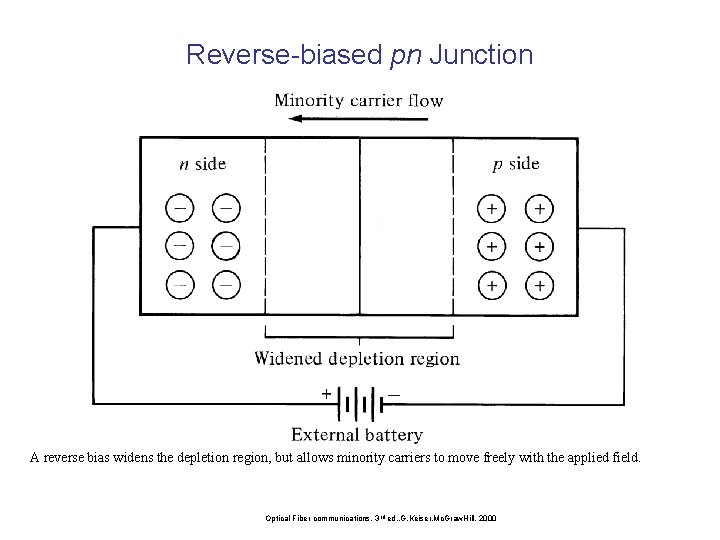
Reverse-biased pn Junction A reverse bias widens the depletion region, but allows minority carriers to move freely with the applied field. Optical Fiber communications, 3 rd ed. , G. Keiser, Mc. Graw. Hill, 2000

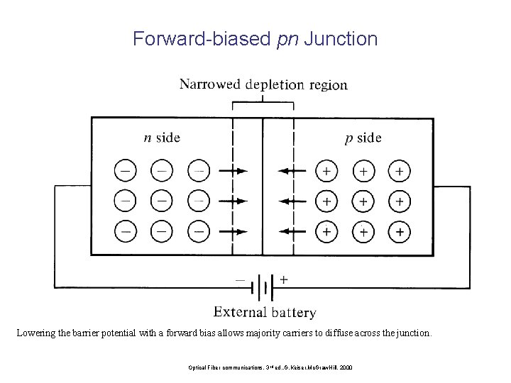
Forward-biased pn Junction Lowering the barrier potential with a forward bias allows majority carriers to diffuse across the junction. Optical Fiber communications, 3 rd ed. , G. Keiser, Mc. Graw. Hill, 2000

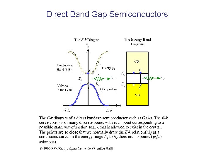
Direct Band Gap Semiconductors

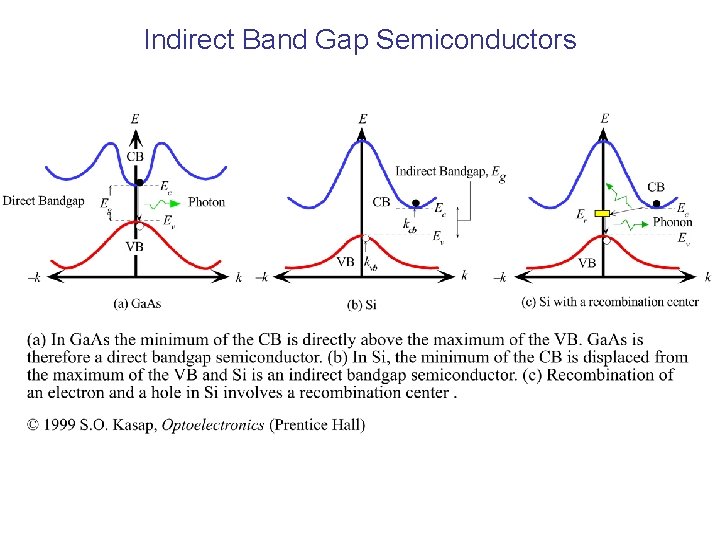
Indirect Band Gap Semiconductors

Light-Emitting Diodes (LEDs) • For photonic communications requiring data rate 100 -200 Mb/s with multimode fiber with tens of microwatts, LEDs are usually the best choice. • LED configurations being used in photonic communications: 1 - Surface Emitters (Front Emitters) 2 - Edge Emitters

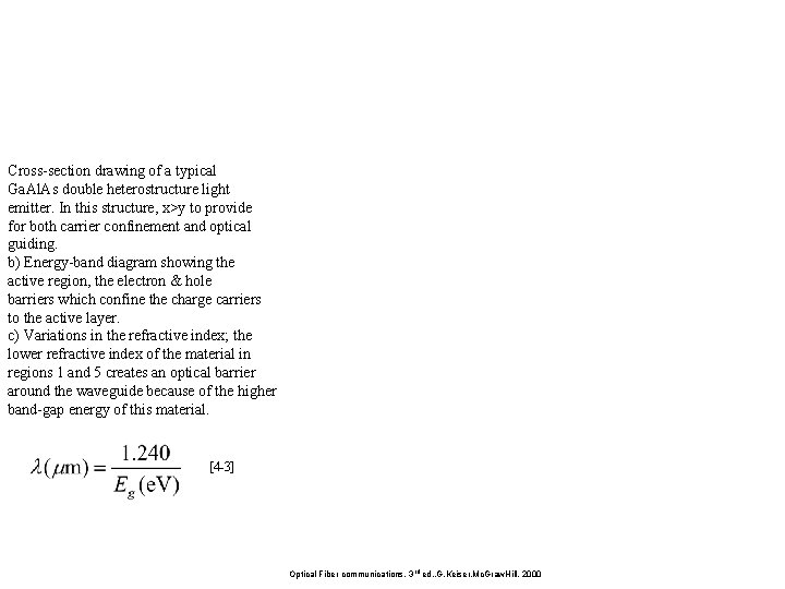
Cross-section drawing of a typical Ga. Al. As double heterostructure light emitter. In this structure, x>y to provide for both carrier confinement and optical guiding. b) Energy-band diagram showing the active region, the electron & hole barriers which confine the charge carriers to the active layer. c) Variations in the refractive index; the lower refractive index of the material in regions 1 and 5 creates an optical barrier around the waveguide because of the higher band-gap energy of this material. [4 -3] Optical Fiber communications, 3 rd ed. , G. Keiser, Mc. Graw. Hill, 2000

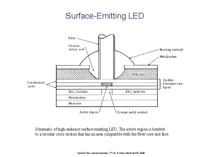
Surface-Emitting LED Schematic of high-radiance surface-emitting LED. The active region is limitted to a circular cross section that has an area compatible with the fiber-core end face. Optical Fiber communications, 3 rd ed. , G. Keiser, Mc. Graw. Hill, 2000

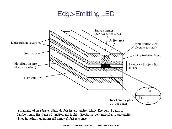
Edge-Emitting LED Schematic of an edge-emitting double heterojunction LED. The output beam is lambertian in the plane of junction and highly directional perpendicular to pn junction. They have high quantum efficiency & fast response. Optical Fiber communications, 3 rd ed. , G. Keiser, Mc. Graw. Hill, 2000

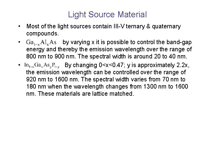
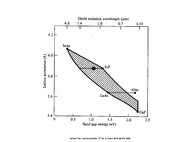
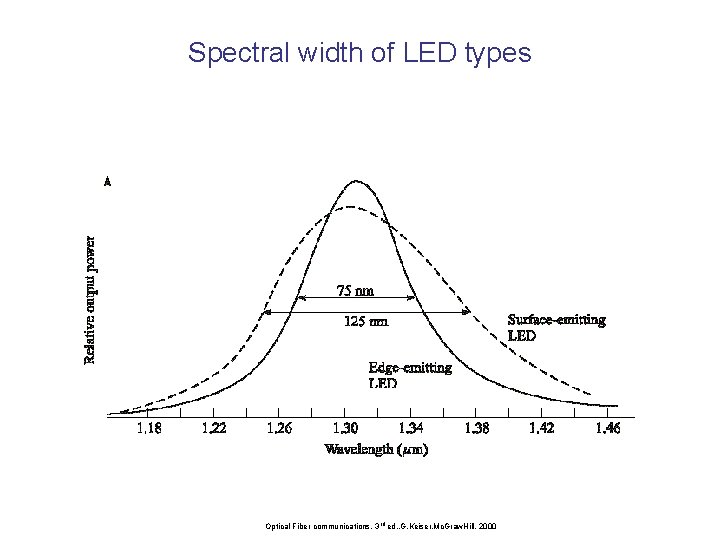
Light Source Material • Most of the light sources contain III-V ternary & quaternary compounds. • by varying x it is possible to control the band-gap energy and thereby the emission wavelength over the range of 800 nm to 900 nm. The spectral width is around 20 to 40 nm. • By changing 0<x<0. 47; y is approximately 2. 2 x, the emission wavelength can be controlled over the range of 920 nm to 1600 nm. The spectral width varies from 70 nm to 180 nm when the wavelength changes from 1300 nm to 1600 nm. These materials are lattice matched.

Optical Fiber communications, 3 rd ed. , G. Keiser, Mc. Graw. Hill, 2000

Spectral width of LED types Optical Fiber communications, 3 rd ed. , G. Keiser, Mc. Graw. Hill, 2000

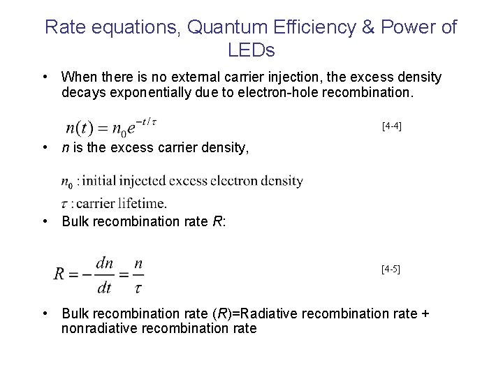
Rate equations, Quantum Efficiency & Power of LEDs • When there is no external carrier injection, the excess density decays exponentially due to electron-hole recombination. [4 -4] • n is the excess carrier density, • Bulk recombination rate R: [4 -5] • Bulk recombination rate (R)=Radiative recombination rate + nonradiative recombination rate

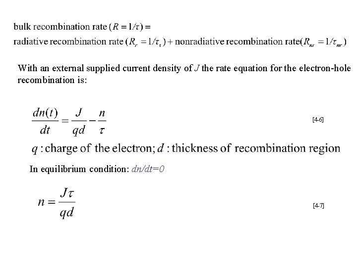
With an external supplied current density of J the rate equation for the electron-hole recombination is: [4 -6] In equilibrium condition: dn/dt=0 [4 -7]
![Internal Quantum Efficiency Optical Power 4 8 Optical power generated internally in the Internal Quantum Efficiency & Optical Power [4 -8] Optical power generated internally in the](https://slidetodoc.com/presentation_image/2a8ed2e40bb0b6bfacce34a97c5da9f4/image-21.jpg)
Internal Quantum Efficiency & Optical Power [4 -8] Optical power generated internally in the active region in the LED is: [4 -9]
![External Quantum Eficiency 4 10 In order to calculate the external quantum efficiency External Quantum Eficiency [4 -10] • In order to calculate the external quantum efficiency,](https://slidetodoc.com/presentation_image/2a8ed2e40bb0b6bfacce34a97c5da9f4/image-22.jpg)
External Quantum Eficiency [4 -10] • In order to calculate the external quantum efficiency, we need to consider the reflection effects at the surface of the LED. If we consider the LED structure as a simple 2 D slab waveguide, only light falling within a cone defined by critical angle will be emitted from an LED.
![4 11 4 12 4 13 4 14 [4 -11] [4 -12] [4 -13] [4 -14]](https://slidetodoc.com/presentation_image/2a8ed2e40bb0b6bfacce34a97c5da9f4/image-23.jpg)
[4 -11] [4 -12] [4 -13] [4 -14]

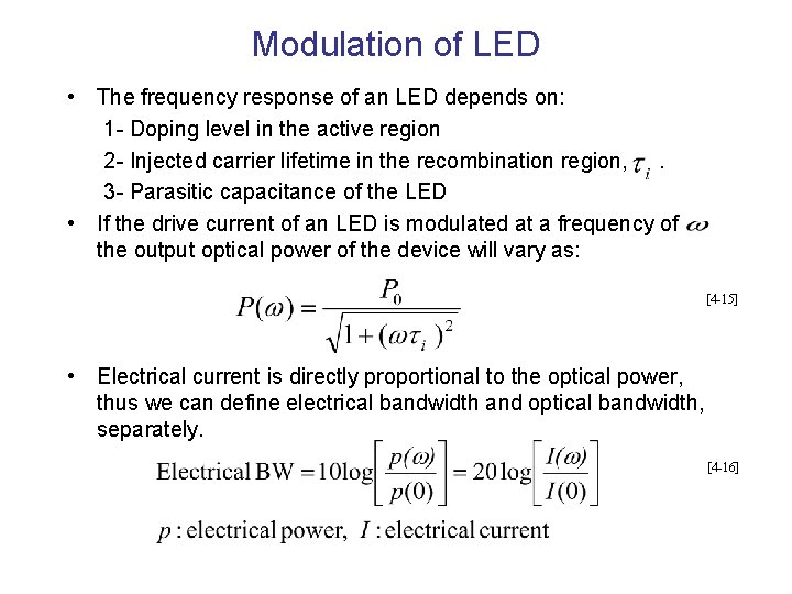
Modulation of LED • The frequency response of an LED depends on: 1 - Doping level in the active region 2 - Injected carrier lifetime in the recombination region, . 3 - Parasitic capacitance of the LED • If the drive current of an LED is modulated at a frequency of the output optical power of the device will vary as: [4 -15] • Electrical current is directly proportional to the optical power, thus we can define electrical bandwidth and optical bandwidth, separately. [4 -16]
![4 17 Optical Fiber communications 3 rd ed G Keiser Mc Graw Hill [4 -17] Optical Fiber communications, 3 rd ed. , G. Keiser, Mc. Graw. Hill,](https://slidetodoc.com/presentation_image/2a8ed2e40bb0b6bfacce34a97c5da9f4/image-25.jpg)
[4 -17] Optical Fiber communications, 3 rd ed. , G. Keiser, Mc. Graw. Hill, 2000