Photodetector on Silicon Heng Yang Outline Introduction Si
- Slides: 17

Photodetector on Silicon Heng Yang

Outline • Introduction • Si Photodetector in 770 ~ 850 nm Range • IR Schottky barrier photodetector

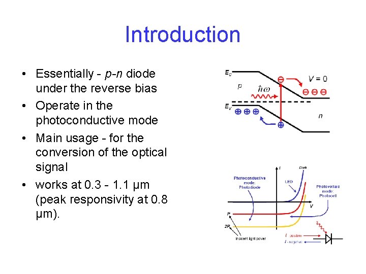
Introduction • Essentially - p-n diode under the reverse bias • Operate in the photoconductive mode • Main usage - for the conversion of the optical signal • works at 0. 3 - 1. 1 µm (peak responsivity at 0. 8 µm).

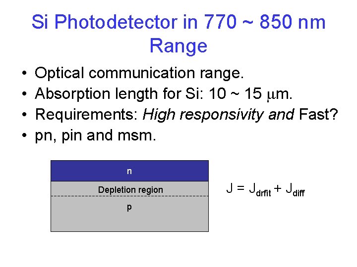
Si Photodetector in 770 ~ 850 nm Range • • Optical communication range. Absorption length for Si: 10 ~ 15 mm. Requirements: High responsivity and Fast? pn, pin and msm. n Depletion region p J = Jdrfit + Jdiff

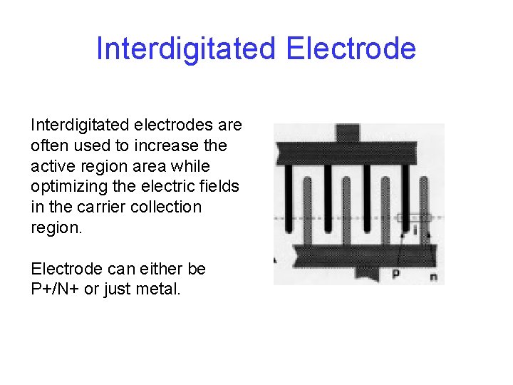
Interdigitated Electrode Interdigitated electrodes are often used to increase the active region area while optimizing the electric fields in the carrier collection region. Electrode can either be P+/N+ or just metal.

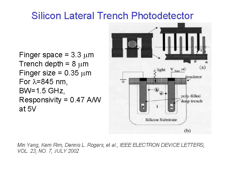
Silicon Lateral Trench Photodetector Finger space = 3. 3 mm Trench depth = 8 mm Finger size = 0. 35 mm For l=845 nm, BW=1. 5 GHz, Responsivity = 0. 47 A/W at 5 V Min Yang, Kern Rim, Dennis L. Rogers, et al. , IEEE ELECTRON DEVICE LETTERS, VOL. 23, NO. 7, JULY 2002

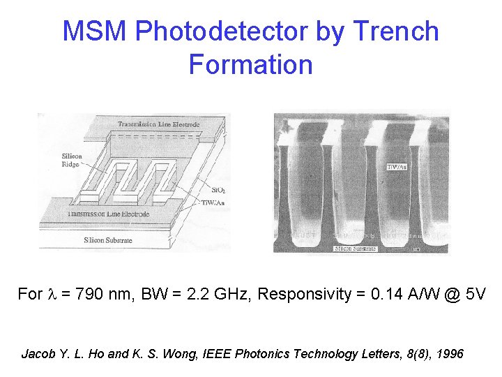
MSM Photodetector by Trench Formation For l = 790 nm, BW = 2. 2 GHz, Responsivity = 0. 14 A/W @ 5 V Jacob Y. L. Ho and K. S. Wong, IEEE Photonics Technology Letters, 8(8), 1996

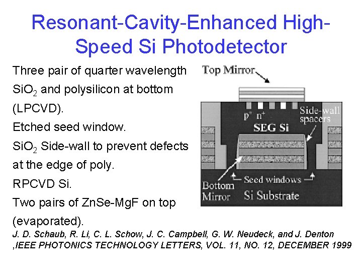
Resonant-Cavity-Enhanced High. Speed Si Photodetector Three pair of quarter wavelength Si. O 2 and polysilicon at bottom (LPCVD). Etched seed window. Si. O 2 Side-wall to prevent defects at the edge of poly. RPCVD Si. Two pairs of Zn. Se-Mg. F on top (evaporated). J. D. Schaub, R. Li, C. L. Schow, J. C. Campbell, G. W. Neudeck, and J. Denton , IEEE PHOTONICS TECHNOLOGY LETTERS, VOL. 11, NO. 12, DECEMBER 1999

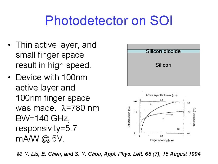
Photodetector on SOI • Thin active layer, and small finger space result in high speed. • Device with 100 nm active layer and 100 nm finger space was made. l=780 nm BW=140 GHz, responsivity=5. 7 m. A/W @ 5 V. Silicon dioxide Silicon M. Y. Liu, E. Chen, and S. Y. Chou, Appl. Phys. Lett. 65 (7), 15 August 1994

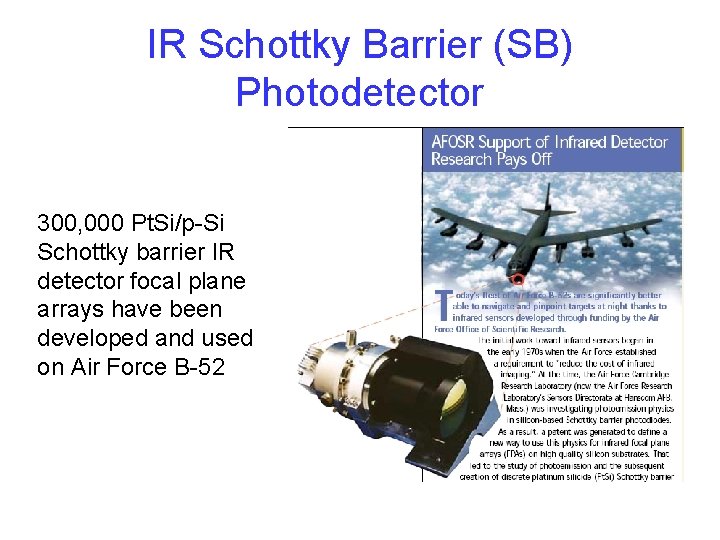
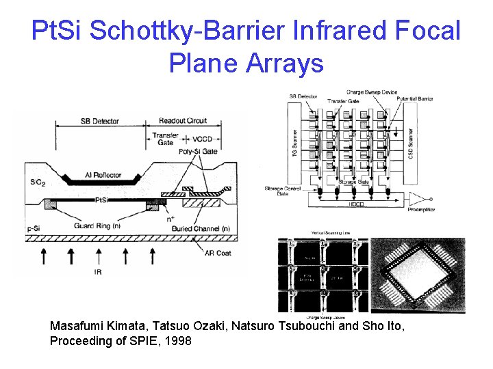
IR Schottky Barrier (SB) Photodetector 300, 000 Pt. Si/p-Si Schottky barrier IR detector focal plane arrays have been developed and used on Air Force B-52

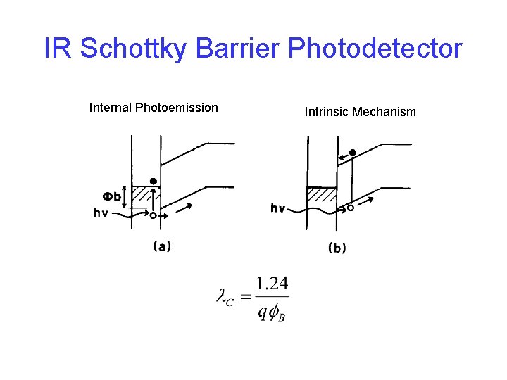
IR Schottky Barrier Photodetector Internal Photoemission Intrinsic Mechanism

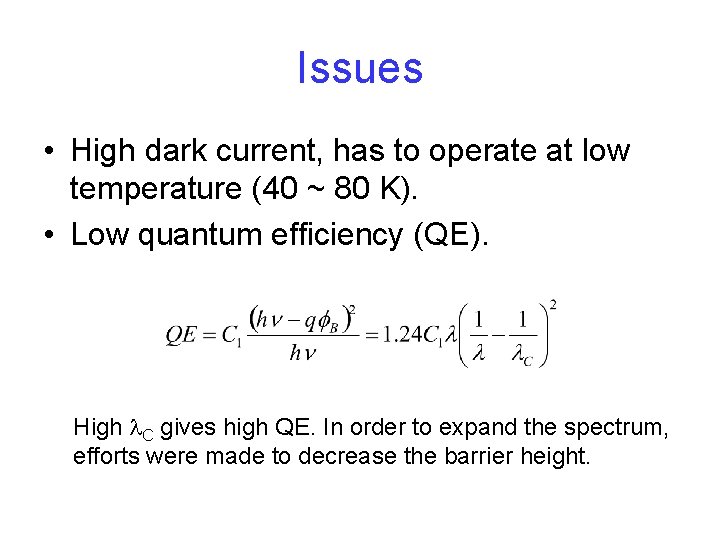
Issues • High dark current, has to operate at low temperature (40 ~ 80 K). • Low quantum efficiency (QE). High l. C gives high QE. In order to expand the spectrum, efforts were made to decrease the barrier height.

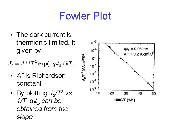
Fowler Plot • The dark current is thermionic limited. It is given by: • A** is Richardson constant • By plotting J 0/T 2 vs 1/T, qf. B can be obtained from the slope.

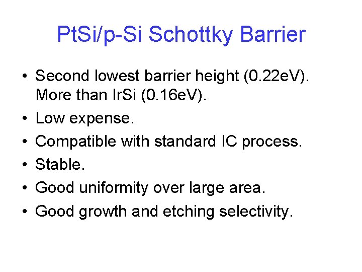
Pt. Si/p-Si Schottky Barrier • Second lowest barrier height (0. 22 e. V). More than Ir. Si (0. 16 e. V). • Low expense. • Compatible with standard IC process. • Stable. • Good uniformity over large area. • Good growth and etching selectivity.

Pt. Si Schottky-Barrier Infrared Focal Plane Arrays Masafumi Kimata, Tatsuo Ozaki, Natsuro Tsubouchi and Sho Ito, Proceeding of SPIE, 1998

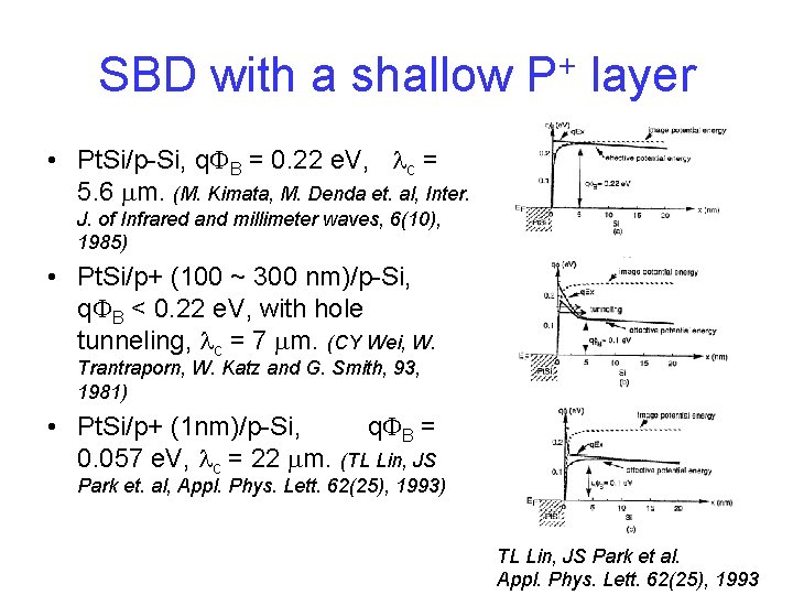
SBD with a shallow P+ layer • Pt. Si/p-Si, q. FB = 0. 22 e. V, lc = 5. 6 mm. (M. Kimata, M. Denda et. al, Inter. J. of Infrared and millimeter waves, 6(10), 1985) • Pt. Si/p+ (100 ~ 300 nm)/p-Si, q. FB < 0. 22 e. V, with hole tunneling, lc = 7 mm. (CY Wei, W. Trantraporn, W. Katz and G. Smith, 93, 1981) • Pt. Si/p+ (1 nm)/p-Si, q. FB = 0. 057 e. V, lc = 22 mm. (TL Lin, JS Park et. al, Appl. Phys. Lett. 62(25), 1993) TL Lin, JS Park et al. Appl. Phys. Lett. 62(25), 1993

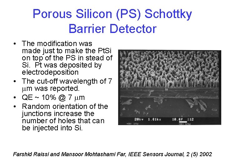
Porous Silicon (PS) Schottky Barrier Detector • The modification was made just to make the Pt. Si on top of the PS in stead of Si. Pt was deposited by electrodeposition • The cut-off wavelength of 7 mm was reported. • QE ~ 10% @ 7 mm • Random orientation of the junctions increase the number of holes that can be injected into Si. Farshid Raissi and Mansoor Mohtashami Far, IEEE Sensors Journal, 2 (5) 2002