Photo Voltaic Materials Outline of presentation 1 PhotoVoltaic

- Slides: 21

Photo Voltaic Materials

Outline of presentation 1. Photo-Voltaic Operation 2. Semi Conductors Materials 3. Shockley Queisser Limits 4. Silicon (Poly/Mono Crystalline, amorphous) 5. Non Silicon based technologies 6. Thin Film

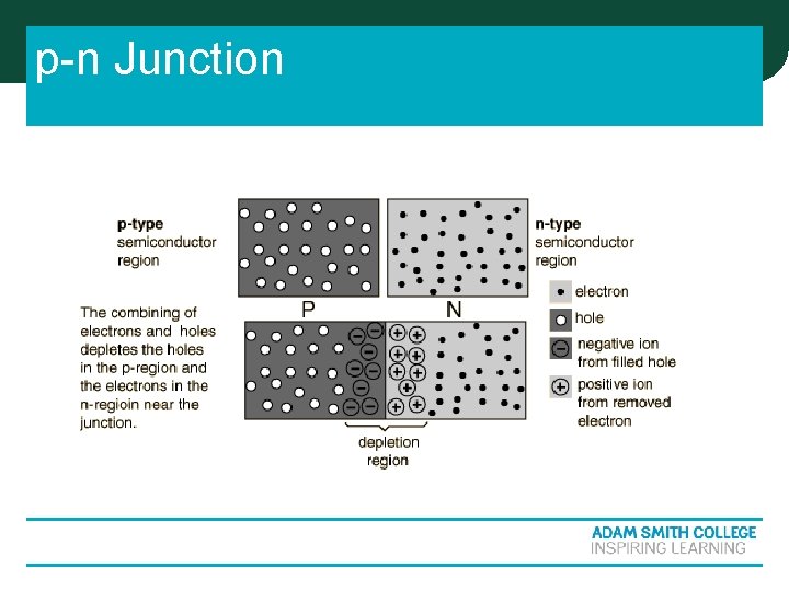
p-n Junction

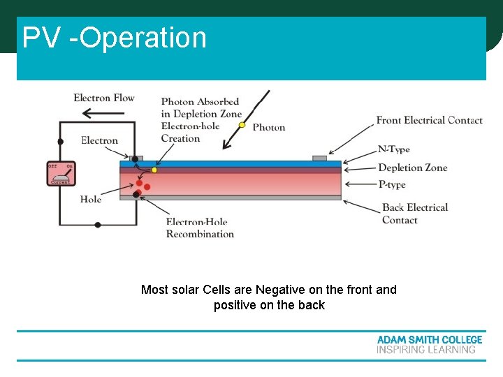
PV -Operation Most solar Cells are Negative on the front and positive on the back

Semi Conductor Semiconductor materials are insulators at absolute zero temperature, but conduct electricity at room temperature. n The defining property of a semiconductor material is that it can be doped with impurities that alter its electronic properties in a controllable way n Semi Conductors can be elemental or compound n

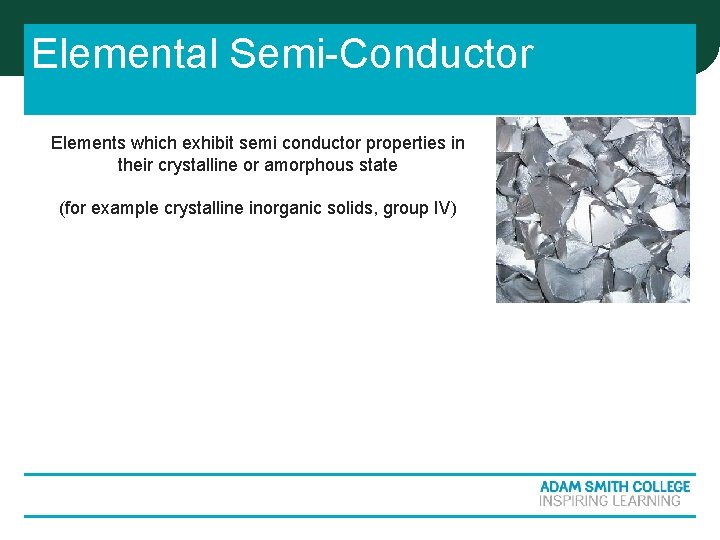
Elemental Semi-Conductor Elements which exhibit semi conductor properties in their crystalline or amorphous state (for example crystalline inorganic solids, group IV)

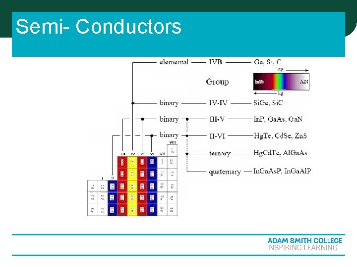
Compound Semi- Conductor n They are formed by using two or more elements. They are synthesized using elements from groups II through VI of the periodic table, e. g. from group III and V (III-V compounds) or II and VI (II-VI compounds). EXAMPLE: n III-V semiconductors: Ga. As, Ga. P, Ga. N, Ga. Al. As, In. P, In. Sb, etc. n II-VI semiconductors: Cd. Se, Cd. Te, Cd. Hg. Te, Zn. S. n

Semi- Conductors

Diversity Advantages Different semiconductor materials differ in their properties. Thus, in comparison with silicon, compound semiconductors have both advantages and disadvantages. n For example, gallium arsenide (Ga. As) has six times higher electron mobility than silicon, which allows faster operation; wider band gap, which allows operation of power devices at higher temperatures, and gives lower thermal noise to low power devices at room temperature; its direct band gap gives it more favourable optoelectronic properties than the indirect band gap of silicon n

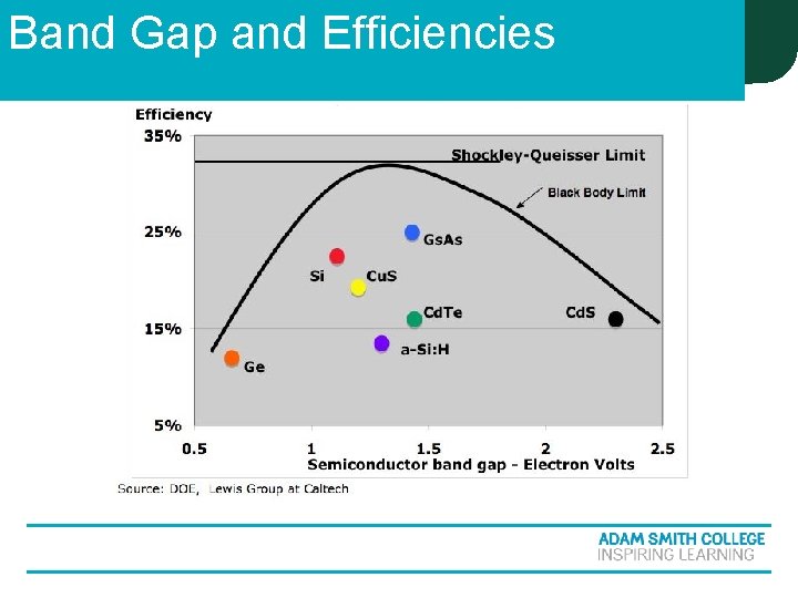
Shockley-Queisser Limits n Limitations - Black Body Emissions - Recombinations - Spectral Losses

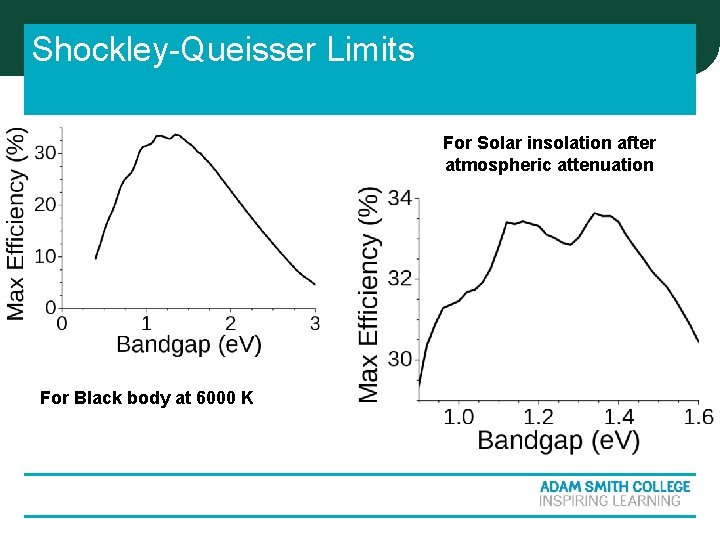
Shockley-Queisser Limits For Solar insolation after atmospheric attenuation For Black body at 6000 K

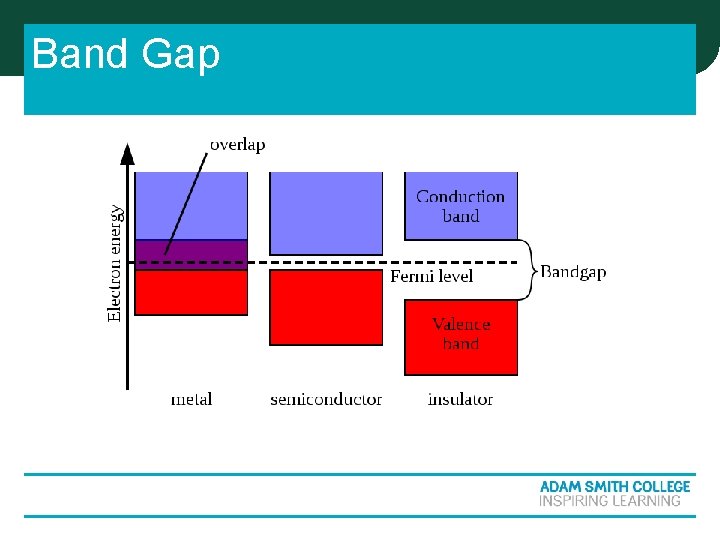
Band Gap

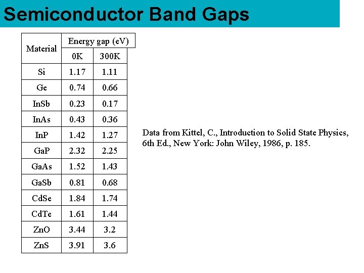
Semiconductor Band Gaps Material Energy gap (e. V) 0 K 300 K Si 1. 17 1. 11 Ge 0. 74 0. 66 In. Sb 0. 23 0. 17 In. As 0. 43 0. 36 In. P 1. 42 1. 27 Ga. P 2. 32 2. 25 Ga. As 1. 52 1. 43 Ga. Sb 0. 81 0. 68 Cd. Se 1. 84 1. 74 Cd. Te 1. 61 1. 44 Zn. O 3. 44 3. 2 Zn. S 3. 91 3. 6 Data from Kittel, C. , Introduction to Solid State Physics, 6 th Ed. , New York: John Wiley, 1986, p. 185.

Band Gap and Efficiencies

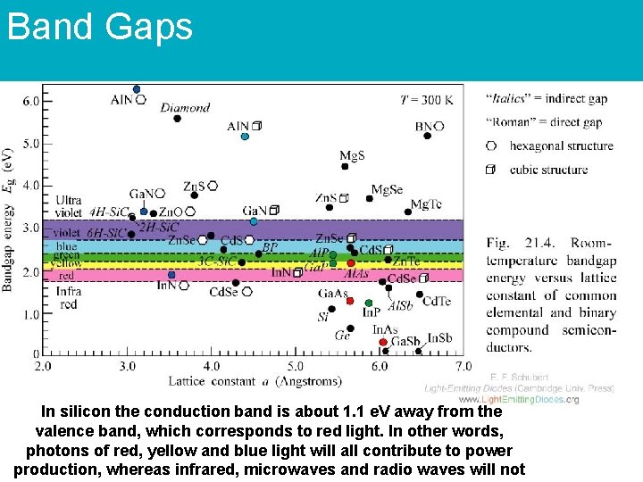
Band Gaps In silicon the conduction band is about 1. 1 e. V away from the valence band, which corresponds to red light. In other words, photons of red, yellow and blue light will all contribute to power production, whereas infrared, microwaves and radio waves will not

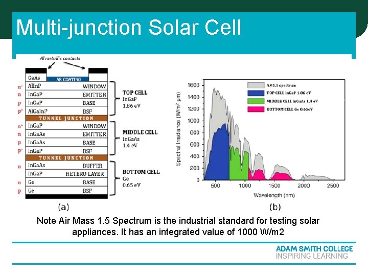
Multi-junction Solar Cell Note Air Mass 1. 5 Spectrum is the industrial standard for testing solar appliances. It has an integrated value of 1000 W/m 2

Crystalline Silicon n n n Widely available, second most abundant element on earths crust after oxygen Is a poor absorber of light and requires several hundred microns of material thickness Occupies over 80% of the world market Is stable, negligible degradation and strong resistant to ionization radiation Wastage is high during mono crystalline silicon production Has advantage of electronics industry backup as silicon is used in chips Efficiencies are high

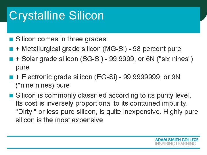
Crystalline Silicon n n Silicon comes in three grades: + Metallurgical grade silicon (MG-Si) - 98 percent pure + Solar grade silicon (SG-Si) - 99. 9999, or 6 N ("six nines") pure + Electronic grade silicon (EG-Si) - 99. 9999999, or 9 N ("nines) pure Silicon is commonly classified according to its purity level. Its cost is inversely proportional to its contained impurity. "Dirty, " or less pure silicon, is quite inexpensive. Highly pure silicon is the most expensive

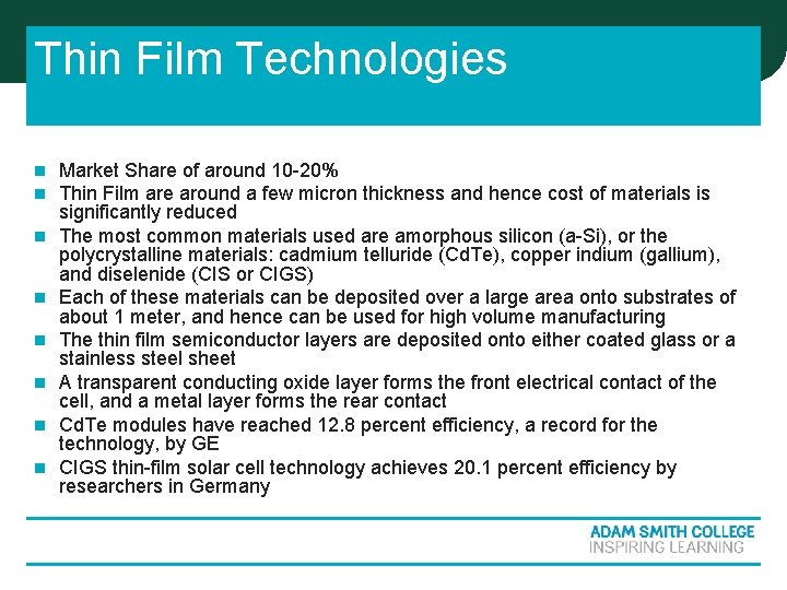
Thin Film Technologies n n n n Market Share of around 10 -20% Thin Film are around a few micron thickness and hence cost of materials is significantly reduced The most common materials used are amorphous silicon (a-Si), or the polycrystalline materials: cadmium telluride (Cd. Te), copper indium (gallium), and diselenide (CIS or CIGS) Each of these materials can be deposited over a large area onto substrates of about 1 meter, and hence can be used for high volume manufacturing The thin film semiconductor layers are deposited onto either coated glass or a stainless steel sheet A transparent conducting oxide layer forms the front electrical contact of the cell, and a metal layer forms the rear contact Cd. Te modules have reached 12. 8 percent efficiency, a record for the technology, by GE CIGS thin-film solar cell technology achieves 20. 1 percent efficiency by researchers in Germany

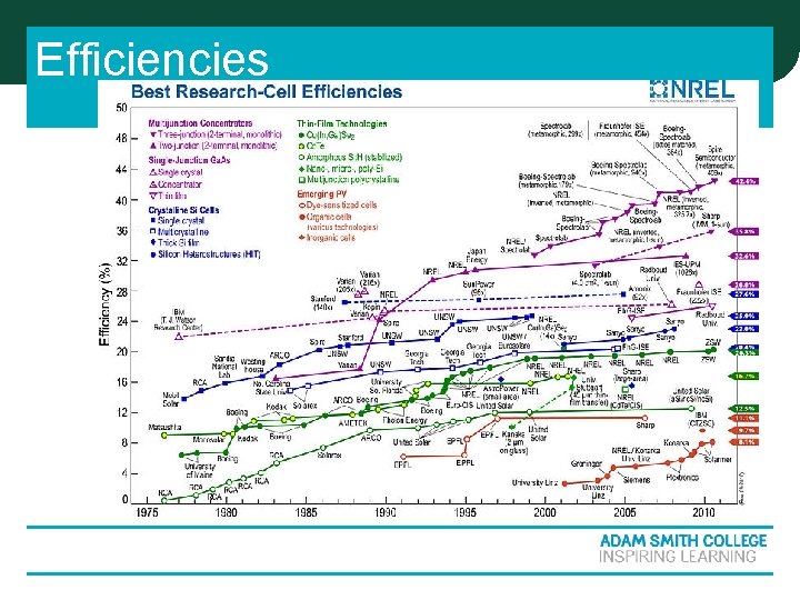
Efficiencies

Sizing PV modules n n n Estimation of Energy Usage Estimation of Solar Resource Estimation of Roof Space Availability of Budget Sizing Batteries