PhaseFrequency Modulators Frequency Modulation using a Voltage Controlled
- Slides: 7

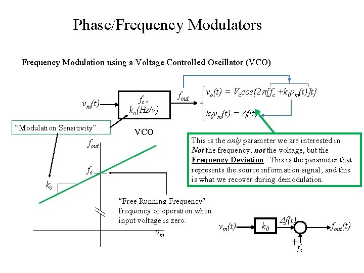
Phase/Frequency Modulators Frequency Modulation using a Voltage Controlled Oscillator (VCO) vm(t) “Modulation Sensitivity” fc , ko(Hz/v) VCO fout vo(t) = Vccos{2 p[fc +k 0 vm(t)]t} k 0 vm(t) = Df(t) This is the only parameter we are interested in! Not the frequency, not the voltage, but the Frequency Deviation. This is the parameter that represents the source information signal; and this is what we recover during demodulation. fout fc ko “Free Running Frequency” frequency of operation when input voltage is zero. vm vm(t) k 0 Df(t) fout(t) + fc

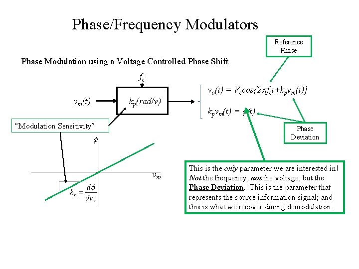
Phase/Frequency Modulators Reference Phase Modulation using a Voltage Controlled Phase Shift fc vo(t) = Vccos{2 pfct+kpvm(t)} vm(t) kp(rad/v) “Modulation Sensitivity” kpvm(t) = f(t) Phase Deviation f vm This is the only parameter we are interested in! Not the frequency, not the voltage, but the Phase Deviation. This is the parameter that represents the source information signal; and this is what we recover during demodulation.

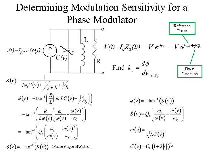
Determining Modulation Sensitivity for a Phase Modulator Reference Phase V(t)=I 0 ZT(t)) = V ejq(t) = V ej(wt+f(t)) i(t)=I 0 cos(wct) Phase Deviation (Phase Angle of Z at wc )

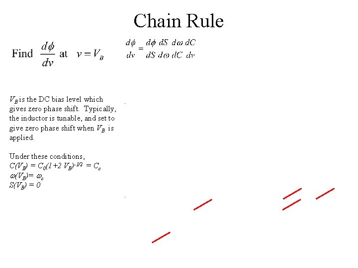
Chain Rule VB is the DC bias level which gives zero phase shift. Typically, the inductor is tunable, and set to give zero phase shift when VB is applied. Under these conditions, C(VB) = C 0(1+2 VB)-1/2 = Cc w(VB)= wc S(VB) = 0

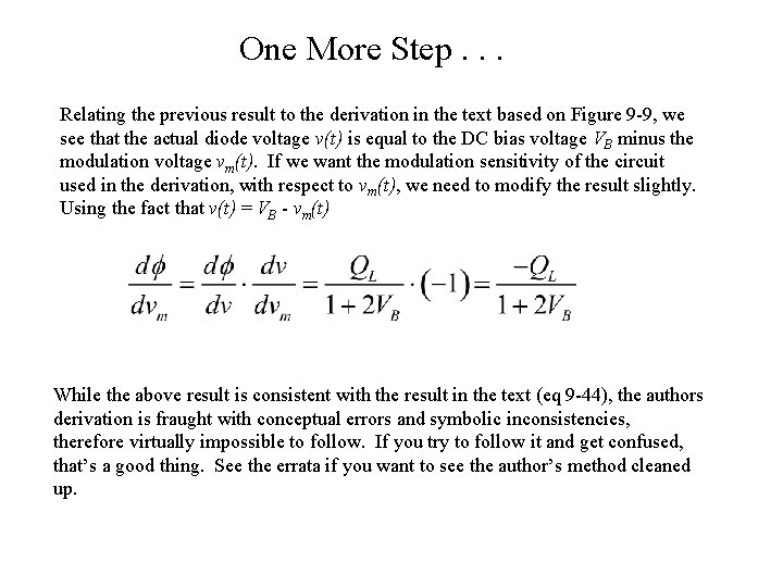
One More Step. . . Relating the previous result to the derivation in the text based on Figure 9 -9, we see that the actual diode voltage v(t) is equal to the DC bias voltage VB minus the modulation voltage vm(t). If we want the modulation sensitivity of the circuit used in the derivation, with respect to vm(t), we need to modify the result slightly. Using the fact that v(t) = VB - vm(t) While the above result is consistent with the result in the text (eq 9 -44), the authors derivation is fraught with conceptual errors and symbolic inconsistencies, therefore virtually impossible to follow. If you try to follow it and get confused, that’s a good thing. See the errata if you want to see the author’s method cleaned up.

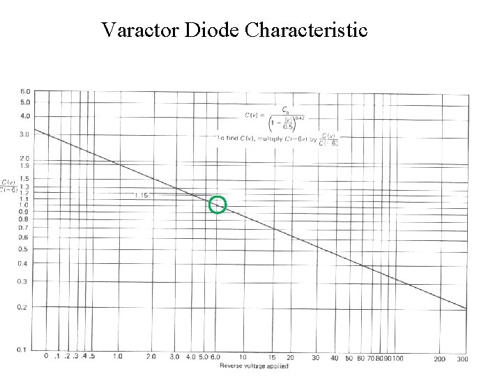
Varactor Diode Characteristic

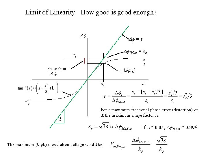
Limit of Linearity: How good is good enough? Df Df = s Df. NOM = se se Df(se) Phase Error Dfe se 1 s For a maximum fractional phase error (distortion) of e, the maximum shape factor is: If e < 0. 05, Df. MAX < 0. 39 R The maximum (0 -pk) modulation voltage would be: