Phase1 Design i PHC System Overview n n

- Slides: 9

Phase-1 Design

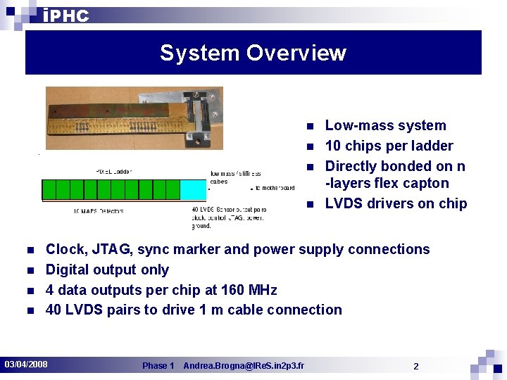
i. PHC System Overview n n n n Low-mass system 10 chips per ladder Directly bonded on n -layers flex capton LVDS drivers on chip Clock, JTAG, sync marker and power supply connections Digital output only 4 data outputs per chip at 160 MHz 40 LVDS pairs to drive 1 m cable connection 03/04/2008 Phase 1 Andrea. Brogna@IRe. S. in 2 p 3. fr 2

i. PHC Preliminary specifications n n n Process 0. 35 µm (AMS c 35 b 4/opto) (3. 3 V ± 0. 3 V) Matrix of 640 x 640 pixels with 30 µm pitch Raw digital output without zero suppression JTAG control for configuration and testing Internal bias DACs 2 levels of multiplexer: Ä n Bonding pad location at the bottom edge Ä n 03/04/2008 Low speed (40 MHz for test) and High speed (160 MHz) Analog test pads (~ 100µm x 100µm) on the top edge Area estimation 19. 5 mm x 21. 0 mm Phase 1 Andrea. Brogna@IRe. S. in 2 p 3. fr 3

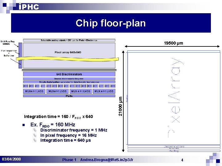
i. PHC Chip floor-plan Integration time = 160 / FRDO x 640 n Ex. FRDO = 160 MHz Ä Ä Ä 03/04/2008 21000 µm 19500 µm Discriminator frequency = 1 MHz In pixel frequency = 16 MHz Integration time = 640 µs Phase 1 Andrea. Brogna@IRe. S. in 2 p 3. fr 4

i. PHC Mimosa 22 background Reuse the experience and building blocks of M 22 n n Best suitable pixel to be chosen from M 22 test Digital control logic Pixel scan => resized to 640 rows Ä Pattern generator => OK Ä n n JTAG interface => markers for synchronizations Output multiplexer with fast/slow outputs Ä n not present in M 22 -- NEW DESIGN Improved Testability for digital and analog blocks 2 registers for test patterns at the discriminator level Ä characterization of pixel matrix Ä 03/04/2008 Phase 1 Andrea. Brogna@IRe. S. in 2 p 3. fr 5

i. PHC Critical points and chip testability n n High speed output @160 MHz Synchronization among the chips in the ladder Internal generation of markers + frame counter Ä How to recovery if chips are out of sync (adding more pins) Ä n n LVDS pads drive 1 m of flex cable Power consumption Static: ~ 400 m. W Ä Dynamic: ~60 m. W (serializ. ); 110 m. W (6 x LVDS TX); 8 m. W (LVDS RX); Ä n Testability based on M 22: Digital: + additional synchronization markers Ä Analog information from groups of 8 columns of pixels Ä 03/04/2008 Phase 1 Andrea. Brogna@IRe. S. in 2 p 3. fr 6

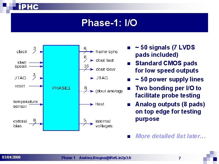
i. PHC Phase-1: I/O n n n 03/04/2008 Phase 1 Andrea. Brogna@IRe. S. in 2 p 3. fr ~ 50 signals (7 LVDS pads included) Standard CMOS pads for low speed outputs ~ 50 power supply lines Two bonding per I/O to facilitate probe testing Analog outputs (8 pads) on top edge for testing purpose More detailed list later… 7

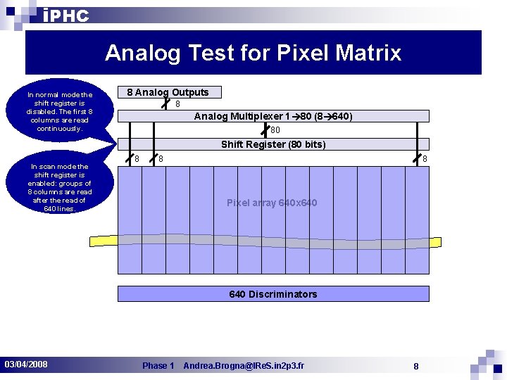
i. PHC Analog Test for Pixel Matrix In normal mode the shift register is disabled. The first 8 columns are read continuously. 8 Analog Outputs 8 Analog Multiplexer 1 80 (8 640) 80 Shift Register (80 bits) In scan mode the shift register is enabled: groups of 8 columns are read after the read of 640 lines. 8 8 8 Pixel array 640 x 640 Discriminators 03/04/2008 Phase 1 Andrea. Brogna@IRe. S. in 2 p 3. fr 8

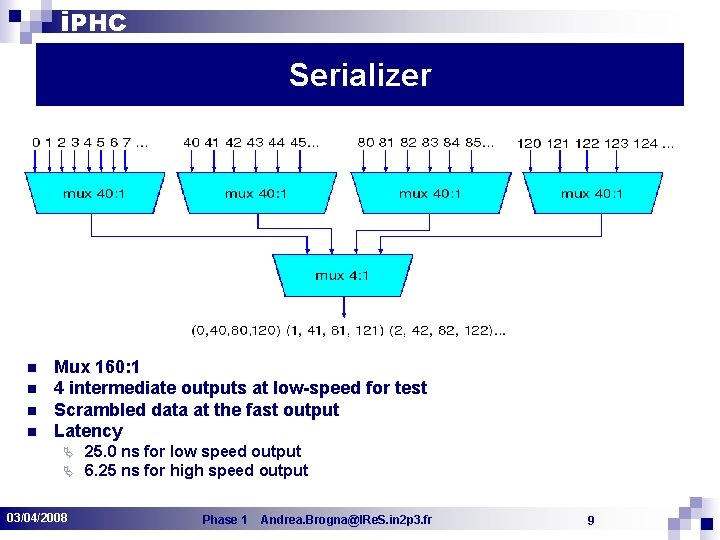
i. PHC Serializer n n Mux 160: 1 4 intermediate outputs at low-speed for test Scrambled data at the fast output Latency Ä Ä 03/04/2008 25. 0 ns for low speed output 6. 25 ns for high speed output Phase 1 Andrea. Brogna@IRe. S. in 2 p 3. fr 9