
Periodic Structures via Laser Matter Interaction Alika Khare

- Slides: 51
Periodic Structures via Laser Matter Interaction Alika Khare Physics Department Indian Institute of Technology Guwahati
Layout • Introduction • Lithography using high power laser Interferometry • Manipulation of atomic trajectories via dipole force • Future Scope • Conclusion • Acknowledgement
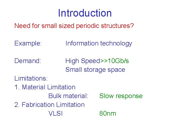
Introduction Need for small sized periodic structures? Example: Information technology Demand: High Speed>>10 Gb/s Small storage space Limitations: 1. Material Limitation Bulk material: 2. Fabrication Limitation VLSI Slow response 80 nm
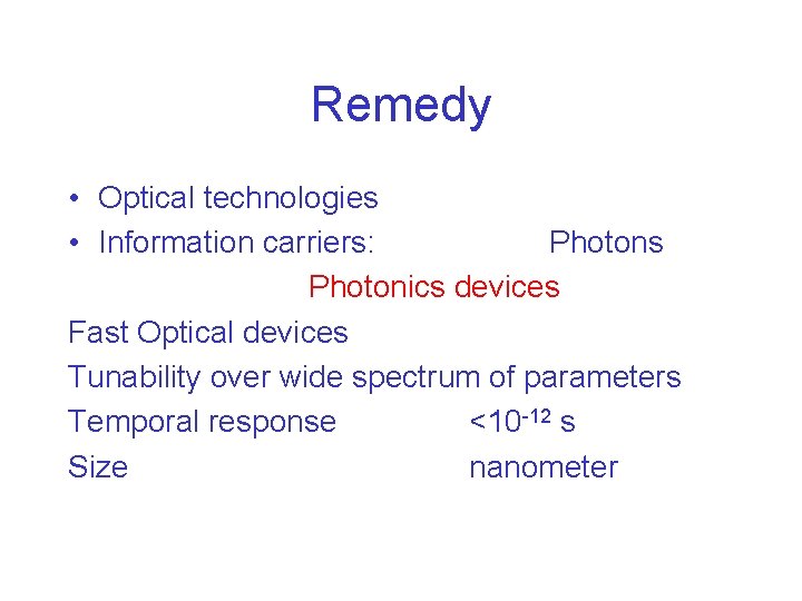
Remedy • Optical technologies • Information carriers: Photons Photonics devices Fast Optical devices Tunability over wide spectrum of parameters Temporal response <10 -12 s Size nanometer
What is to be done? • Synthesis of new Materials • Materials having periodic structures dimensions <100 nm • Quantum confinement effect Drastic changes in optical, electrical mechanical, thermal and magnetic characteristics of the materials from its bulk behaviour and offers the tremendous scope in microelectronics, optoelectronics and Photonics industries.
Manipulation of the materials via Laser Matter Interaction • Modification into surface morphology via selective laser ablation of thin films • Modification into the trajectories of atom via dipole force
Lithography using High Power Laser Interferometry • Selective ablation of Thin films Modification into the surface morphology of the orders of tens of nm. Two step process • a. Deposition of thin films b. Selective ablation Single step Simple set-up
a. Deposition of thin film • Techniques used • Thermal Evaporation technique • Pulsed Laser Deposition Technique
Thin films used • Thermal evaporation Indium and chromium thin films
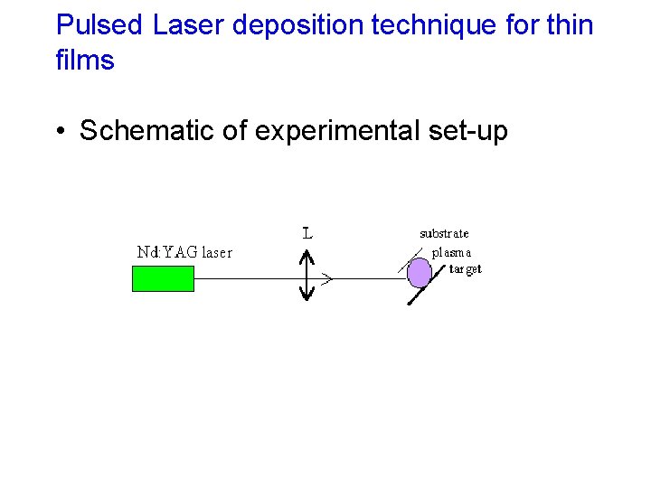
Pulsed Laser deposition technique for thin films • Schematic of experimental set-up
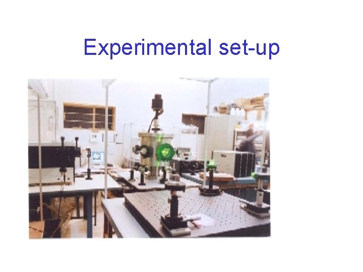
Experimental set-up
Advantages of PLD • Applicable to any material • Applicable to any form of the target material: Solid Liquid Gas • By controlling the environment any composition can be deposited
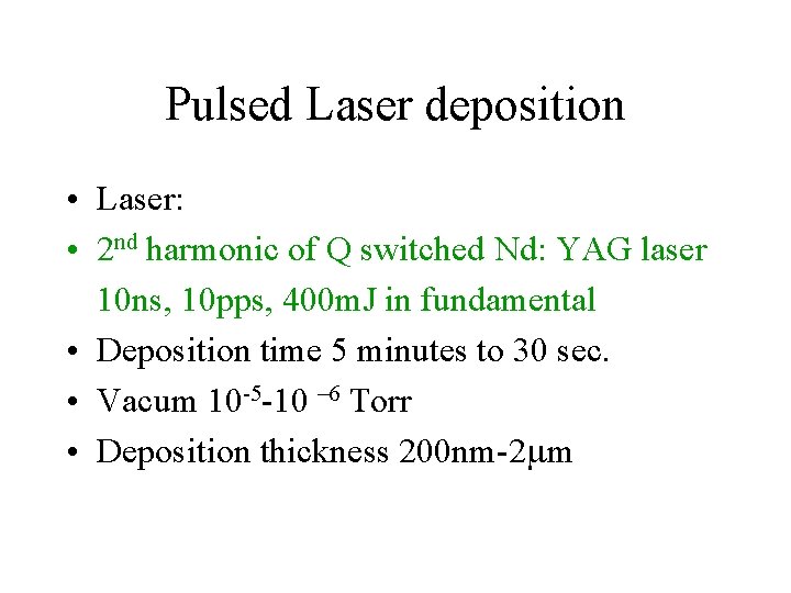
Pulsed Laser deposition • Laser: • 2 nd harmonic of Q switched Nd: YAG laser 10 ns, 10 pps, 400 m. J in fundamental • Deposition time 5 minutes to 30 sec. • Vacum 10 -5 -10 – 6 Torr • Deposition thickness 200 nm-2 m
Target Material • Copper • Silicon wafer • Zinc Oxide
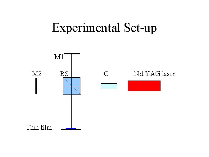
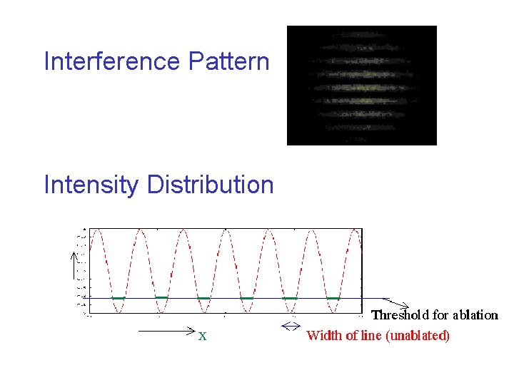
b. Selective Ablation of thin films by High Power Laser Interferometry • The thin films can be selectively ablated by illumination with the interference pattern form by High power laser Interferometer.
Experimental Set-up
Interference Pattern Intensity Distribution
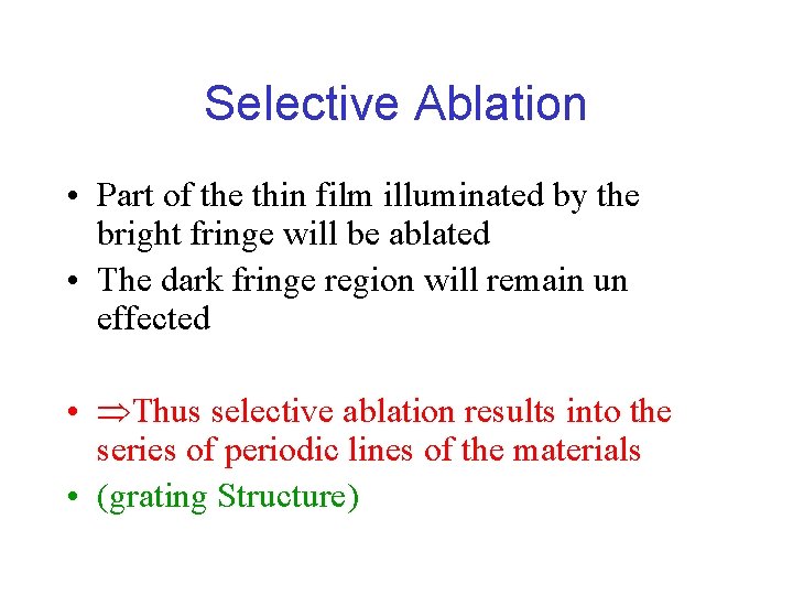
Selective Ablation • Part of the thin film illuminated by the bright fringe will be ablated • The dark fringe region will remain un effected • Thus selective ablation results into the series of periodic lines of the materials • (grating Structure)
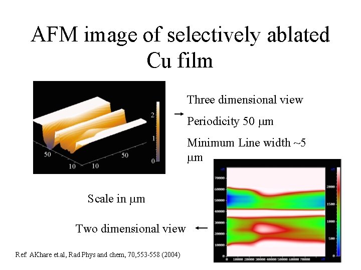
AFM image of selectively ablated Cu film Three dimensional view Periodicity 50 m Minimum Line width ~5 m Scale in m Two dimensional view Ref: AKhare et. al, Rad Phys and chem, 70, 553 -558 (2004)
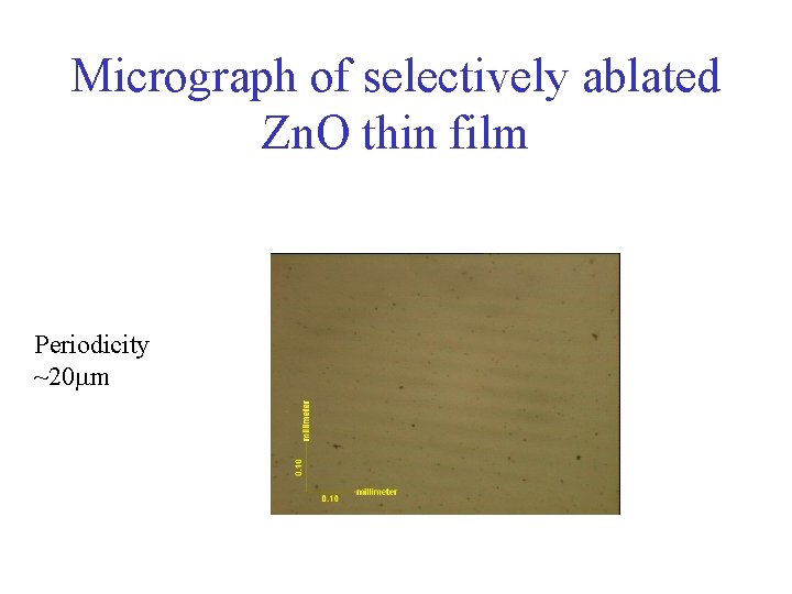
Micrograph of selectively ablated Zn. O thin film Periodicity ~20 m
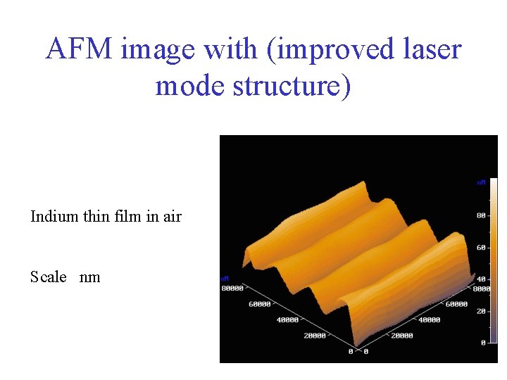
AFM image with (improved laser mode structure) Indium thin film in air Scale nm
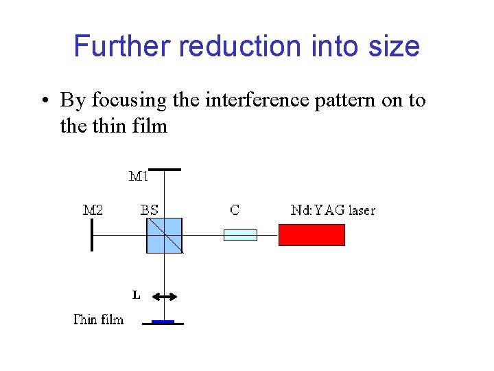
Further reduction into size • By focusing the interference pattern on to the thin film L
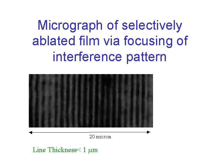
Micrograph of selectively ablated film via focusing of interference pattern Line Thickness< 1 m
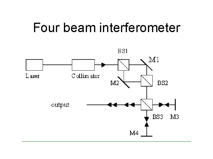
Formation of two dimensional arrays • Two interferometer in tandem • Out put of one interferometer illuminates the second stage of interferometer Four beam interference Square arrays of two dimensional light spot
Four beam interferometer
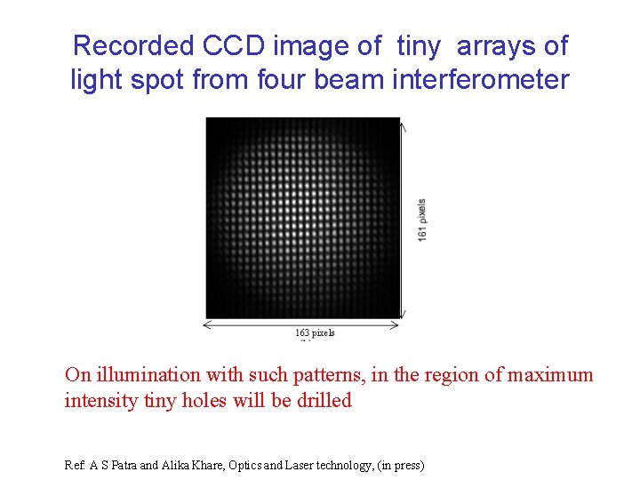
Recorded CCD image of tiny arrays of light spot from four beam interferometer On illumination with such patterns, in the region of maximum intensity tiny holes will be drilled Ref: A S Patra and Alika Khare, Optics and Laser technology, (in press)
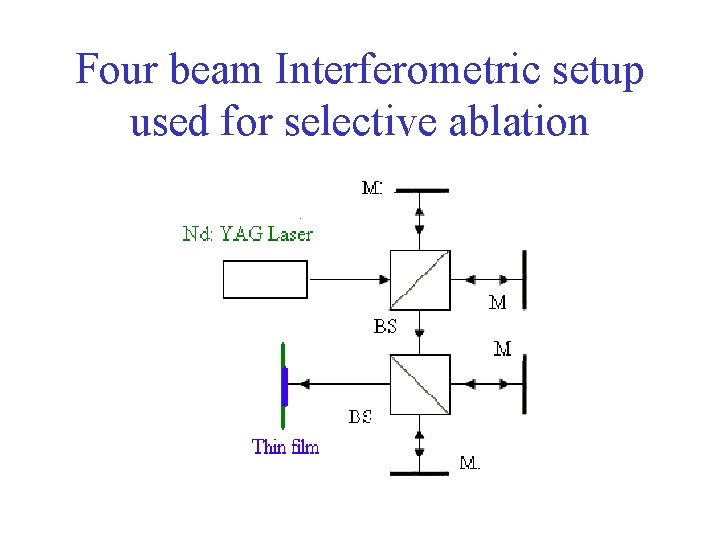
Four beam Interferometric setup used for selective ablation
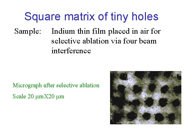
Square matrix of tiny holes Sample: Indium thin film placed in air for selective ablation via four beam interference Micrograph after selective ablation Scale 20 m. X 20 m
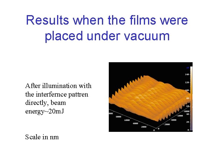
Results when the films were placed under vacuum After illumination with the interfernce pattren directly, beam energy~20 m. J Scale in nm
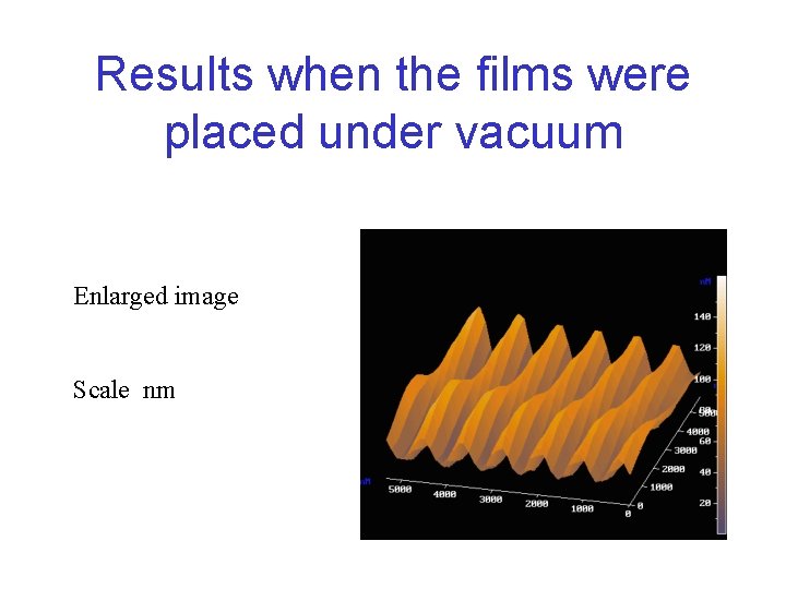
Results when the films were placed under vacuum Enlarged image Scale nm
Advantage of the technique • Applicable to any material • Complete writing in Single step, Single shot • Structure size tens of nanometer • Relatively simple
Limitation of the selective ablation via high power laser interferometer • Periodicity ~
What is to be done to reduce the periodicity? • Manipulation of Atomic Trajectories using Dipole force
Origin of dipole force Interaction of induced dipole moment with non-uniform near resonant light distribution.
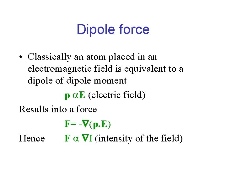
Dipole force • Classically an atom placed in an electromagnetic field is equivalent to a dipole of dipole moment p E (electric field) Results into a force F= - (p. E) Hence F I (intensity of the field)
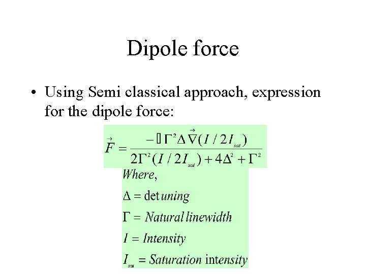
Dipole force • Using Semi classical approach, expression for the dipole force:
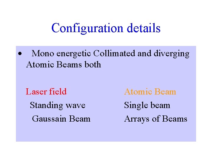
Configuration details · Mono energetic Collimated and diverging Atomic Beams both Laser field Atomic Beam Standing wave Single beam Gaussain Beam Arrays of Beams
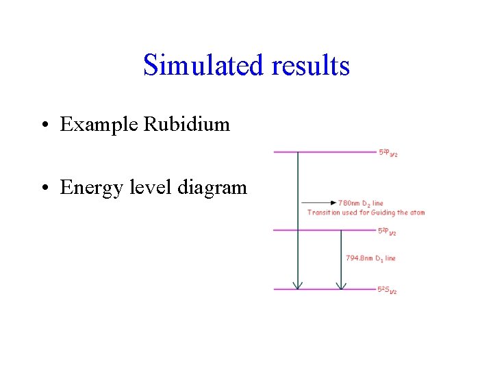
Simulated results • Example Rubidium • Energy level diagram
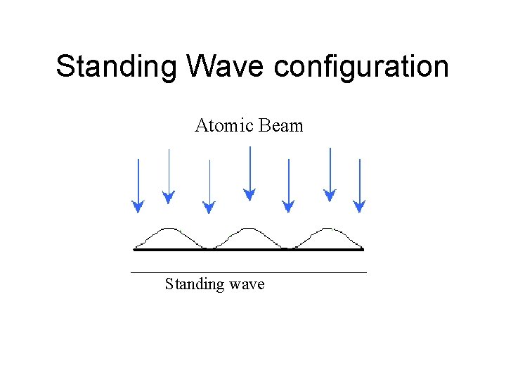
Standing Wave configuration Atomic Beam Standing wave
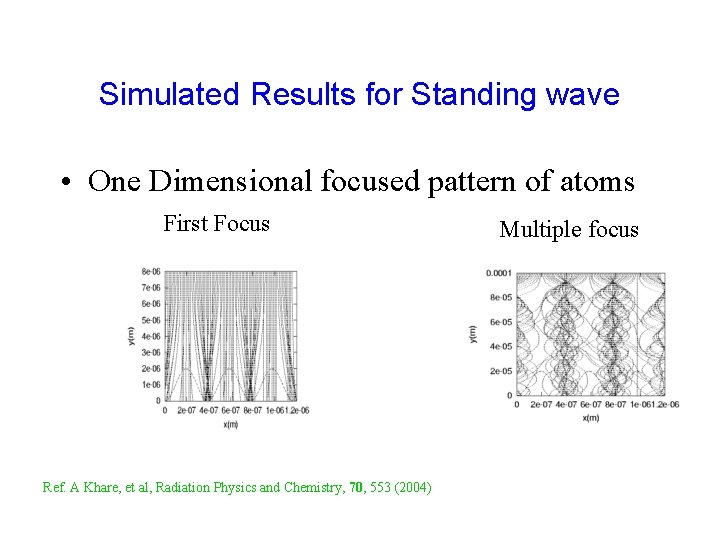
Simulated Results for Standing wave • One Dimensional focused pattern of atoms First Focus Ref. A Khare, et al, Radiation Physics and Chemistry, 70, 553 (2004) Multiple focus
Limitation • Periodicity /2
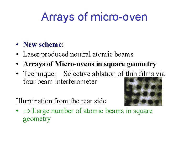
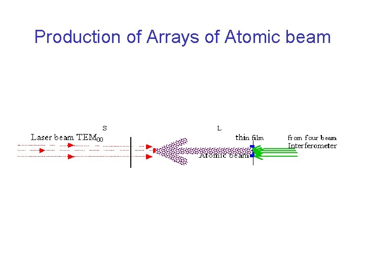
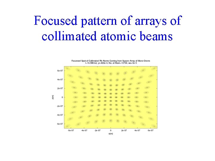
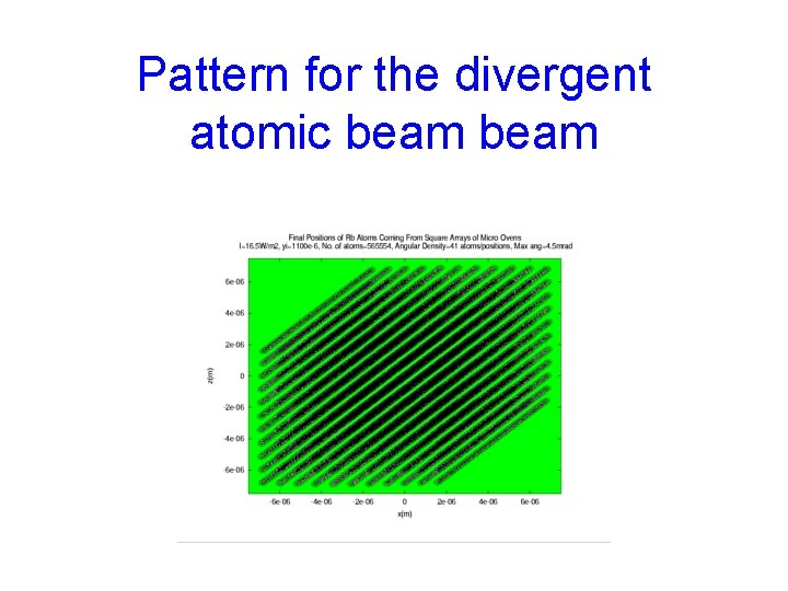
Arrays of micro-oven • • New scheme: Laser produced neutral atomic beams Arrays of Micro-ovens in square geometry Technique: Selective ablation of thin films via four beam interferometer Illumination from the rear side • Large number of atomic beams in square geometry
Production of Arrays of Atomic beam
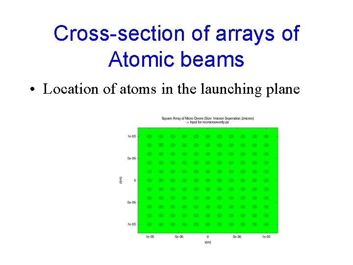
Cross-section of arrays of Atomic beams • Location of atoms in the launching plane
Focused pattern of arrays of collimated atomic beams
Pattern for the divergent atomic beam
Future Scope Selective ablation technique is very general and can be applied on any material with any high power laser Formation of • Tiny Arrays of laser • Wave guide • Optocoupler • Photonic band gap material
Future scope • The manipulation of atoms via dipole force is a coming up field where the process has to be understood fully, involving the atom laser interaction. The concept of series of micro-oven is yet to be perfected experimentally. Periodicity and line width both can be reduced by appropriate choice of atomic beam system and laser field.
Conclusion • Two schemes based on Laser matter interaction for the generation of periodic small structures • Selective ablation via high power laser interferometer periodicity 1 m • Simulated pattern for the dipole force using multiple atomic beam • Periodicity as well as spot size ~tens of nm
Acknowledgement • 1. Research Scholars • Mr AS Patra and Mr Kamlesh Alti • 2. Partial financial assistance from • i. CSIR, New Delhi, India, Scheme No. 03(831)/98/EMR-II • ii. MHRD, New Delhi, India Scheme No. F. 26 -1/2000/TSV
Thank you