PDMS An Example of a Versatile Material for
- Slides: 44

PDMS: An Example of a Versatile Material for Micro- and Nanotechnology www. nano 4 me. org © 2018 The Pennsylvania State University PDMS 1

Outline • • Background Properties of PDMS Applications of PDMS Modification of PDMS www. nano 4 me. org © 2018 The Pennsylvania State University PDMS 2

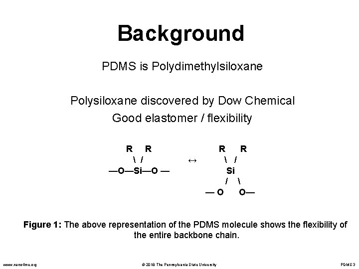
Background PDMS is Polydimethylsiloxane Polysiloxane discovered by Dow Chemical Good elastomer / flexibility R R / —O—Si—O — R R ↔ / Si / —O O— Figure 1: The above representation of the PDMS molecule shows the flexibility of the entire backbone chain. www. nano 4 me. org © 2018 The Pennsylvania State University PDMS 3

Background • • • There at least six forms of commercially viable PDMS products that are common: Fluids Emulsions Compounds Lubricants Resins Elastomers or rubbers www. nano 4 me. org © 2018 The Pennsylvania State University PDMS 4

Background • As shown in the last slide PDMS has many forms and uses. It is especially useful because it is relatively inexpensive. • Our focus will be on PDMS as a “substrate”. It is especially useful for microfluidics. • Another very good example of a PDMS application is soft contact lens. – The lenses are inexpensive, have exacting tolerances, and must be biocompatible. www. nano 4 me. org © 2018 The Pennsylvania State University PDMS 5

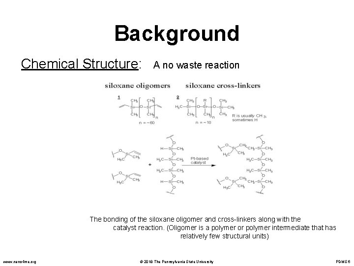
Background Chemical Structure: A no waste reaction The bonding of the siloxane oligomer and cross-linkers along with the catalyst reaction. (Oligomer is a polymer or polymer intermediate that has relatively few structural units) www. nano 4 me. org © 2018 The Pennsylvania State University PDMS 6

Outline • • Background Properties of PDMS Applications of PDMS Modification of PDMS www. nano 4 me. org © 2018 The Pennsylvania State University PDMS 7

Properties of PDMS - Its unique surface properties such as low surface tension are ideal for : Paper release agents, fiber lubricants, textile hand modifiers, mold release agents, anti-fouling materials and water repellents. - It is transparent, pliant, biocompatible, permeable to oxygen, chemically inert, homogeneous, and has low water absorption. Hydrophobicity can be altered to suit the application. - Resistant to sunlight, moisture, heat, cold, aging, or weather. www. nano 4 me. org © 2018 The Pennsylvania State University PDMS 8

Properties of PDMS The ratio of base to curing agent, is a 2 part mixture: 1: 1 or 10: 1 Room temperature curing may take a full day, or fast curing is accomplished using heat. Safety Issues: Benign National Fire Protection Agency (NFPA) rating: Cure - Health -0 Flammability – 0 Instability/reactivity – 1 Base – Health – 0 Flammability – 1 Instability/reactivity – 0 Overexposure risk is minimal www. nano 4 me. org © 2018 The Pennsylvania State University PDMS 9

PDMS Form Sylgard-184 • Mixture of the curing agent and the base components in a 10: 1 ratio (by weight). • De-gas the mixture by vacuum to draw air to the surface. • Curing for 24 hours at 23°C; 4 hours at 65°C; 1 hour at 100°C; or 15 minutes at 150°C. www. nano 4 me. org © 2018 The Pennsylvania State University PDMS 10

Cost of PDMS – Pricing of a ½ Kilo of PDMS (approx. 1. 1 lbs. ) $40. 00 Equipment – Spinner @ $6 k – 8 k Squeegee or similar device under $10. 00 Hot Plate for under $500 PDMS has a shelf life of 24 months for an unopened container from the date of manufacture. www. nano 4 me. org © 2018 The Pennsylvania State University PDMS 11

Suppliers of PDMS • Sigma-Aldrich - Poly(dimethylsiloxane) • Dow Corning - Sylgard 184 • Polysciences Inc. - Poly(dimethylsiloxane) www. nano 4 me. org © 2018 The Pennsylvania State University PDMS 12

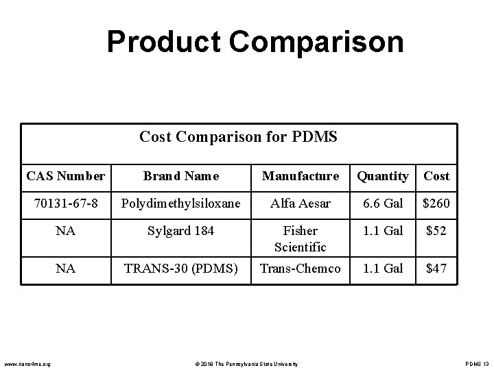
Product Comparison Cost Comparison for PDMS CAS Number Brand Name Manufacture Quantity Cost 70131 -67 -8 Polydimethylsiloxane Alfa Aesar 6. 6 Gal $260 NA Sylgard 184 Fisher Scientific 1. 1 Gal $52 NA TRANS-30 (PDMS) Trans-Chemco 1. 1 Gal $47 www. nano 4 me. org © 2018 The Pennsylvania State University PDMS 13

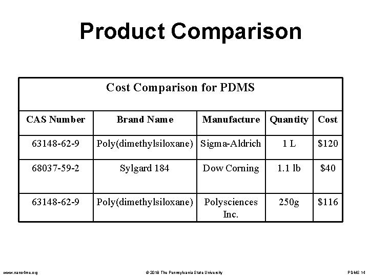
Product Comparison Cost Comparison for PDMS CAS Number 63148 -62 -9 Brand Name Manufacture Quantity Cost Poly(dimethylsiloxane) Sigma-Aldrich 1 L $120 68037 -59 -2 Sylgard 184 Dow Corning 1. 1 lb $40 63148 -62 -9 Poly(dimethylsiloxane) Polysciences Inc. 250 g $116 www. nano 4 me. org © 2018 The Pennsylvania State University PDMS 14

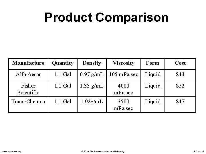
Product Comparison Manufacture Quantity Alfa Aesar 1. 1 Gal Fisher Scientific Trans-Chemco www. nano 4 me. org Density Viscosity Form Cost 0. 97 g/m. L 105 m. Pa. sec Liquid $43 1. 1 Gal 1. 33 g/m. L 4000 m. Pa. sec Liquid $52 1. 1 Gal 1. 02 g/m. L 3500 m. Pa. sec Liquid $47 © 2018 The Pennsylvania State University PDMS 15

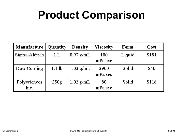
Product Comparison Manufacture Quantity Density Viscosity Form Cost Sigma-Aldrich 1 L 0. 97 g/m. L 100 m. Pa. sec Liquid $181 Dow Corning 1. 1 lb 1. 03 g/m. L 3900 m. Pa. sec Solid $40 Polysciences Inc. 250 g 1. 02 g/m. L 80 m. Pa. sec Solid $116 www. nano 4 me. org © 2018 The Pennsylvania State University PDMS 16

Outline • • Background Properties of PDMS Applications of PDMS Modification of PDMS www. nano 4 me. org © 2018 The Pennsylvania State University PDMS 17

Applications of PDMS • • PDMS Stamp Fabrication Methods Various Soft Lithography Techniques Microfluidic Channel Casting Implanted Biomedical Microsystems www. nano 4 me. org © 2018 The Pennsylvania State University PDMS 18

PDMS Stamps Using SU-8 Resist • Commonly used to fabricate polymeric microfluidic structures. • SU-8 has high a viscosity, and the ability to define layers between 1 and 200μm with high aspect ratio and vertical sidewalls. • SU-8 is patterned with contact lithography. The PDMS mixture is added on the SU-8 master, cured, and then, peeled off. www. nano 4 me. org © 2018 The Pennsylvania State University PDMS 19

Soft Lithography • Use of elastomeric stamps or molds to transfer patterns onto a surface with different techniques: – – – www. nano 4 me. org Microcontact printing (μCP) Replica Molding (REM) Microtransfer Molding (μTM) Micromolding in Capillaries (MIMIC) Solvent-assisted Micromolding (SAMIM) High Aspect Ratio Microstructure Replication (HARM) © 2018 The Pennsylvania State University PDMS 20

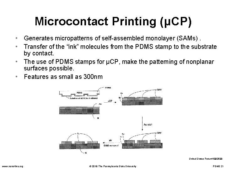
Microcontact Printing (μCP) • Generates micropatterns of self-assembled monolayer (SAMs). • Transfer of the “ink” molecules from the PDMS stamp to the substrate by contact. • The use of PDMS stamps for μCP, make the patterning of nonplanar surfaces possible. • Features as small as 300 nm United States Patent 6890598 www. nano 4 me. org © 2018 The Pennsylvania State University PDMS 21

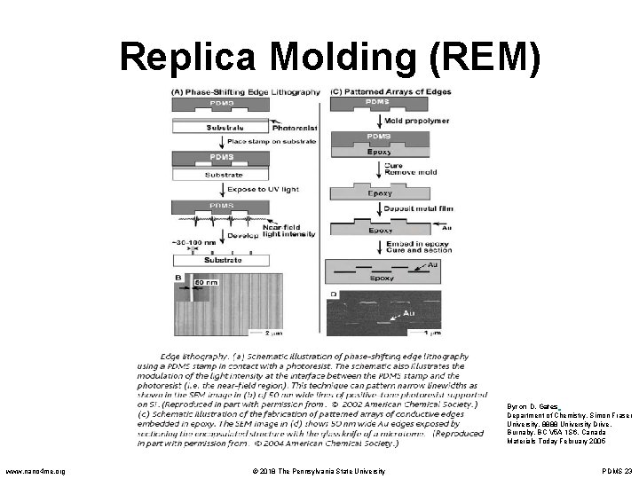
Replica Molding (REM) • Uses a PDMS stamp as the master to duplicate molds. Polyurethane (PU) is then molded in the PDMS master. • Sizes and shapes may be changed in a controlled way (mechanical compression, bending, or stretching). • Ability to fabricate structures of ~30 nm in organic polymers. www. nano 4 me. org © 2018 The Pennsylvania State University PDMS 22

Replica Molding (REM) Byron D. Gates Department of Chemistry, Simon Fraser University, 8888 University Drive, Burnaby, BC V 5 A 1 S 6, Canada Materials Today February 2005 www. nano 4 me. org © 2018 The Pennsylvania State University PDMS 23

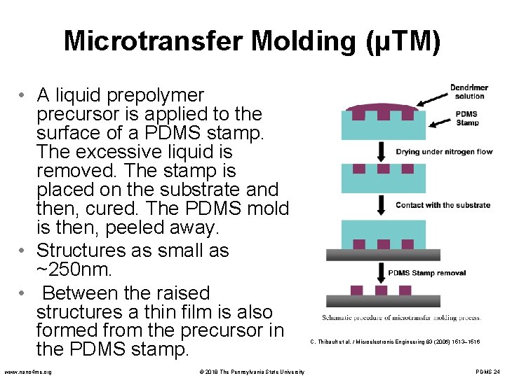
Microtransfer Molding (μTM) • A liquid prepolymer precursor is applied to the surface of a PDMS stamp. The excessive liquid is removed. The stamp is placed on the substrate and then, cured. The PDMS mold is then, peeled away. • Structures as small as ~250 nm. • Between the raised structures a thin film is also formed from the precursor in the PDMS stamp. www. nano 4 me. org © 2018 The Pennsylvania State University C. Thibault et al. / Microelectronic Engineering 83 (2006) 1513– 1516 PDMS 24

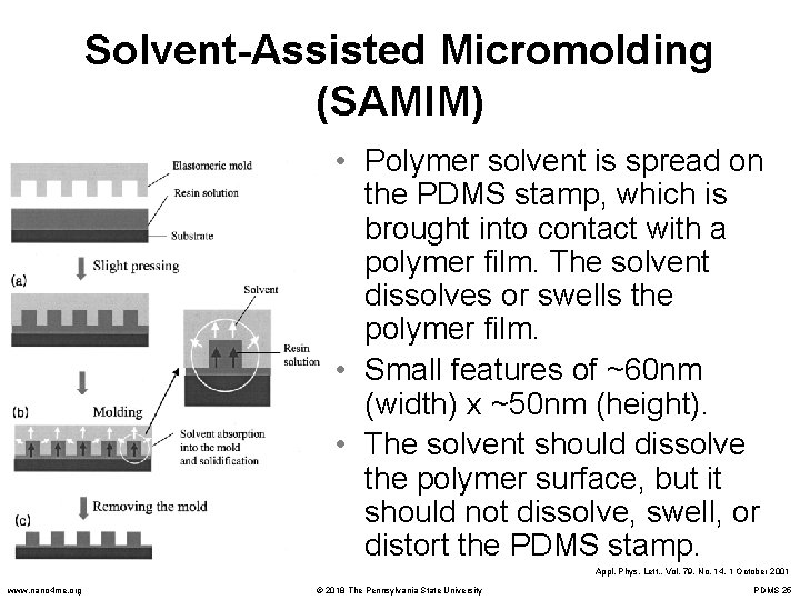
Solvent-Assisted Micromolding (SAMIM) • Polymer solvent is spread on the PDMS stamp, which is brought into contact with a polymer film. The solvent dissolves or swells the polymer film. • Small features of ~60 nm (width) x ~50 nm (height). • The solvent should dissolve the polymer surface, but it should not dissolve, swell, or distort the PDMS stamp. Appl. Phys. Lett. , Vol. 79, No. 14, 1 October 2001 www. nano 4 me. org © 2018 The Pennsylvania State University PDMS 25

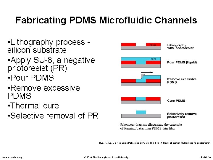
Fabricating PDMS Microfluidic Channels • Lithography process silicon substrate • Apply SU-8, a negative photoresist (PR) • Pour PDMS • Remove excessive PDMS • Thermal cure • Selective removal of PR Ryu, K. , Liu, Ch. “Precision Patterning of PDMS Thin Film: A New Fabrication Method and its applications” www. nano 4 me. org © 2018 The Pennsylvania State University PDMS 26

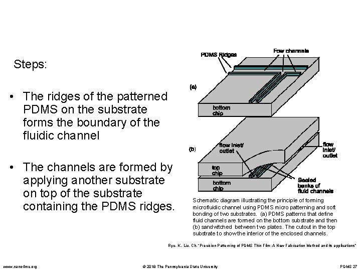
Steps: • The ridges of the patterned PDMS on the substrate forms the boundary of the fluidic channel • The channels are formed by applying another substrate on top of the substrate containing the PDMS ridges. Schematic diagram illustrating the principle of forming microfluidic channel using PDMS micro patterning and soft bonding of two substrates. (a) PDMS patterns that define fluid channels are formed on the bottom substrate and then (b) sandwitched between two plates. The cutout in the top substrate to show the interior of the enclosed channels. Ryu, K. , Liu, Ch. “Precision Patterning of PDMS Thin Film: A New Fabrication Method and its applications” www. nano 4 me. org © 2018 The Pennsylvania State University PDMS 27

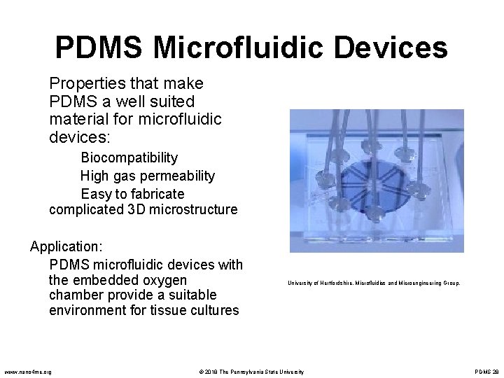
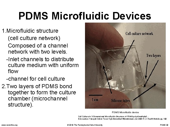
PDMS Microfluidic Devices Properties that make PDMS a well suited material for microfluidic devices: Biocompatibility High gas permeability Easy to fabricate complicated 3 D microstructure Application: PDMS microfluidic devices with the embedded oxygen chamber provide a suitable environment for tissue cultures www. nano 4 me. org University of Hertfordshire. Microfluidics and Microengineering Group. © 2018 The Pennsylvania State University PDMS 28

PDMS Microfluidic Devices 1. Microfluidic structure (cell culture network) Composed of a channel network with two levels. -Inlet channels to distribute culture medium with uniform flow -channel for cell culture 2. Two layers of PDMS bond together to form the culture chamber (microchannel structure). PDMS Microfluidic device Cell Culture in 3 -Dimensional Microfluidic Structure of PDMS polydimethylsil. . . Eric Leclerc; Yasuyuki Sakai; Teruo Fujii Biomedical Microdevices; Jun 2003; 5, 2; Health Module pg. 109 www. nano 4 me. org © 2018 The Pennsylvania State University PDMS 29

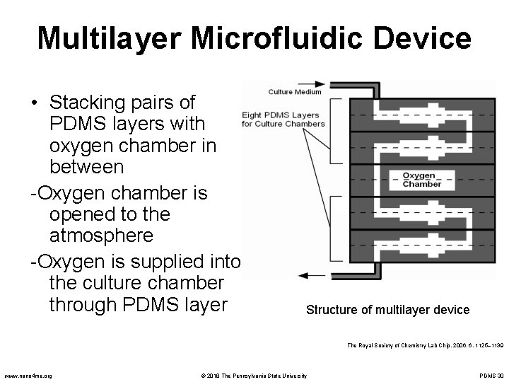
Multilayer Microfluidic Device • Stacking pairs of PDMS layers with oxygen chamber in between -Oxygen chamber is opened to the atmosphere -Oxygen is supplied into the culture chamber through PDMS layer Structure of multilayer device The Royal Society of Chemistry Lab Chip, 2006, 6, 1125– 1139 www. nano 4 me. org © 2018 The Pennsylvania State University PDMS 30

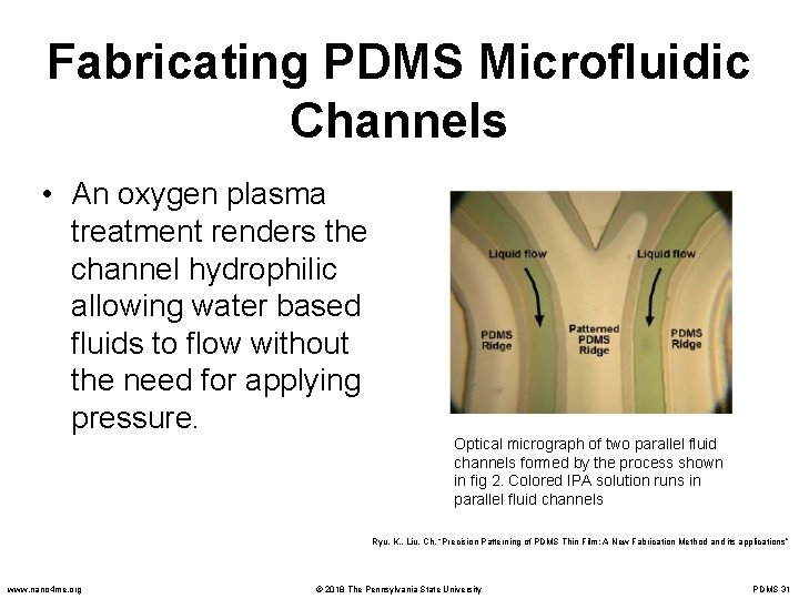
Fabricating PDMS Microfluidic Channels • An oxygen plasma treatment renders the channel hydrophilic allowing water based fluids to flow without the need for applying pressure. Optical micrograph of two parallel fluid channels formed by the process shown in fig 2. Colored IPA solution runs in parallel fluid channels Ryu, K. , Liu, Ch. “Precision Patterning of PDMS Thin Film: A New Fabrication Method and its applications” www. nano 4 me. org © 2018 The Pennsylvania State University PDMS 31

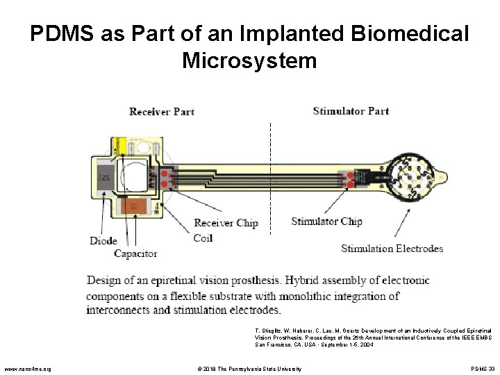
PDMS as Part of an Implanted Biomedical Microsystem Retinal Prosthesis – Stimulating retinal neurons. • A high dynamic range external CMOS camera sends images to an encoder in spatio-temporal stimulation patterns. • These patterns match the input of the ganglion cell layer in an intact retina. • A data decoding chip stimulates the proper retina cells electronically, which cause them to send action potentials to the brain via the optical nerve. T. Stieglitz, W. Haberer, C. Lau, M. Goertz Development of an Inductively Coupled Epiretinal Vision Prosthesis. Proceedings of the 26 th Annual International Conference of the IEEE EMBS San Francisco, CA, USA • September 1 -5, 2004 www. nano 4 me. org © 2018 The Pennsylvania State University PDMS 32

PDMS as Part of an Implanted Biomedical Microsystem T. Stieglitz, W. Haberer, C. Lau, M. Goertz Development of an Inductively Coupled Epiretinal Vision Prosthesis. Proceedings of the 26 th Annual International Conference of the IEEE EMBS San Francisco, CA, USA • September 1 -5, 2004 www. nano 4 me. org © 2018 The Pennsylvania State University PDMS 33

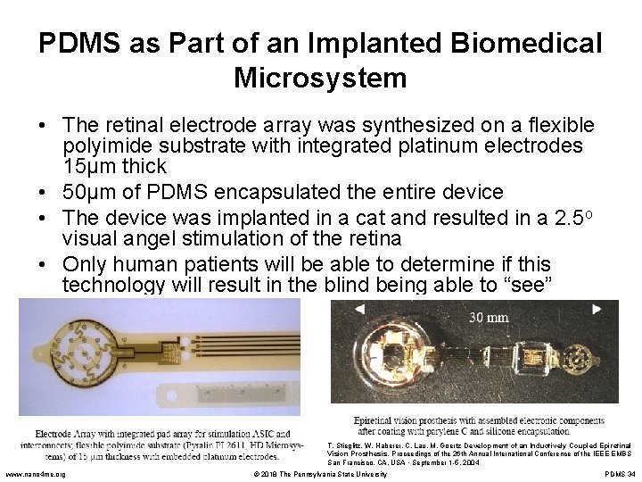
PDMS as Part of an Implanted Biomedical Microsystem • The retinal electrode array was synthesized on a flexible polyimide substrate with integrated platinum electrodes 15µm thick • 50µm of PDMS encapsulated the entire device • The device was implanted in a cat and resulted in a 2. 5 o visual angel stimulation of the retina • Only human patients will be able to determine if this technology will result in the blind being able to “see” T. Stieglitz, W. Haberer, C. Lau, M. Goertz Development of an Inductively Coupled Epiretinal Vision Prosthesis. Proceedings of the 26 th Annual International Conference of the IEEE EMBS San Francisco, CA, USA • September 1 -5, 2004 www. nano 4 me. org © 2018 The Pennsylvania State University PDMS 34

Outline • • Background Properties of PDMS Applications of PDMS Modification of PDMS www. nano 4 me. org © 2018 The Pennsylvania State University PDMS 35

PDMS Modification • Some PDMS applications require surface modification in order to improve the wettability and adhesion properties of PDMS surfaces. – Oxygen Plasma. – UV Light and Ozone (UVO). Efimenko, K. , Wallace, W. E. , and Genzer, J. “Surface Modification of Sylgard-184 Poly(Dimethyl Diloxane) Networkds by Ultraviolet and Ultraviolet/Ozone Treatment. ” Journal of Colloid and Interface Science. 2002, 254, 306 -315. www. nano 4 me. org © 2018 The Pennsylvania State University PDMS 36

Oxygen Plasma • Reactive Ion Etch (RIE) oxygen plasma, has been the most widely used technique. • Oxygen atoms substitute methyl groups on the PDMS surface leading to the formation of hydrophilic surfaces. Carbon pumped away as CO 2 and H 2 O. • Modified surfaces of PDMS can be used to bond glass, silicon substrates and other PDMS molds or structures Efimenko, K. , Wallace, W. E. , and Genzer, J. “Surface Modification of Sylgard-184 Poly(Dimethyl Diloxane) Networkds by Ultraviolet and Ultraviolet/Ozone Treatment. ” Journal of Colloid and Interface Science. 2002, 254, 306 -315. www. nano 4 me. org © 2018 The Pennsylvania State University PDMS 37

UV Light and UV Light + Ozone (UVO) • UV light increases Si-O concentration, forming a silica-like substrate. • UVO is more effective than UV in creating hydrophilic groups because of the molecular oxygen and ozone present, which forms a larger number of hydrophilic species (OH). B. Schnyder et al. / Surface Science 532– 535 (2003) 1067– 1071 www. nano 4 me. org © 2018 The Pennsylvania State University PDMS 38

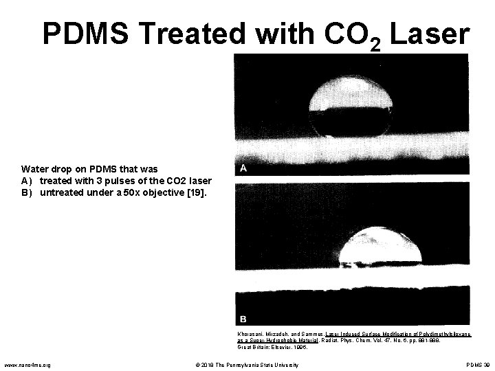
PDMS Treated with CO 2 Laser Water drop on PDMS that was A) treated with 3 pulses of the CO 2 laser B) untreated under a 50 x objective [19]. Khorasani, Mirzadeh, and Sammes. Laser Induced Surface Modification of Polydimethylsiloxane as a Super-Hydrophobic Material. Radiat. Phys. Chem. Vol. 47, No. 6, pp. 881 -888. Great Britain: Elsevier, 1996. www. nano 4 me. org © 2018 The Pennsylvania State University PDMS 39

PDMS Bonding Importance of PDMS bonding – Low temperature bonding Bonding process : Standard lithography technique • Spin deposition of PDMS • Exposure with 420 nm Ultra Violet light • Brief exposure to oxygen plasma cure (at 20 m. Torr and 25 W, for 20 seconds) • Immediately join to glass, Si. O 2 or PDMS itself (with in 10 min) Long exposure to plasma roughens the PDMS surface and interferes with bonding www. nano 4 me. org © 2018 The Pennsylvania State University PDMS 40

Advantages of PDMS • Optical transparency (wavelength from 230 to 700 nm makes it suitable for UV/ visible spectrophotometry). • Permeable to variety of liquids and vapors (allows it to absorb a variety of compounds). • Conforms to the surface of the substrate over a relatively large area • Conformal contact achievable on nonplanar surfaces • Can be released easily, even from complex and fragile structures • Low cost. • Simple fabrication process. www. nano 4 me. org © 2018 The Pennsylvania State University PDMS 41

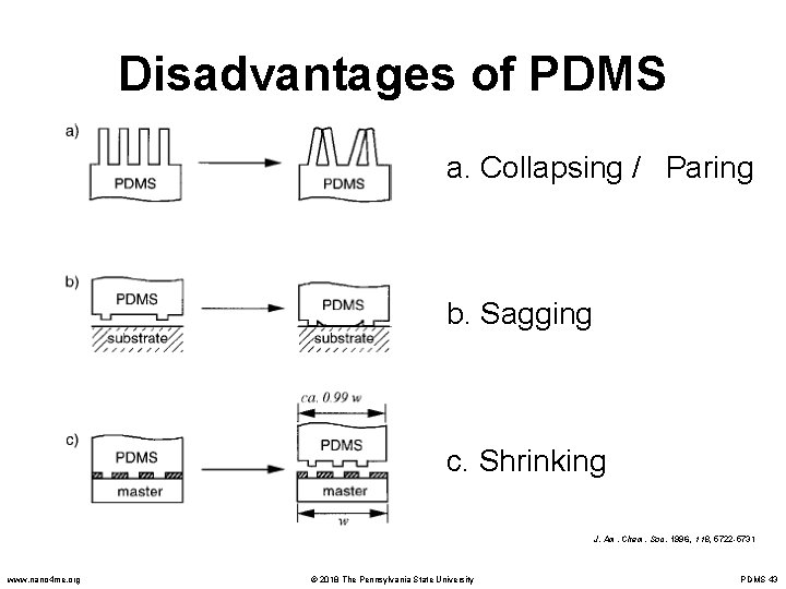
Disadvantages of PDMS • Wide and shallow micro channels can easily collapse during the bonding process. • Because PDMS is easily deformable, the technology is not well suited for devices that require precise pattern placement. • PDMS stamps also tend to shrink to a factor of 1% upon curing. • Some relief structures are not able to resist the compressive forces of printing and the adhesion between the stamp and the substrate, which leads to sagging. www. nano 4 me. org © 2018 The Pennsylvania State University PDMS 42

Disadvantages of PDMS a. Collapsing / Paring b. Sagging c. Shrinking J. Am. Chem. Soc. 1996, 118, 5722 -5731 www. nano 4 me. org © 2018 The Pennsylvania State University PDMS 43

Summary of PDMS • 70 year technology with present and future applications in micro and nanofabrication such as microfluidics and biomedical applications • Spun, wiped or pour deposited • Heat decreased curing time • Soft, pliable, clear, safe, easy to use and inexpensive • 24 month shelf life from date of manufacture www. nano 4 me. org © 2018 The Pennsylvania State University PDMS 44