PCI and PCIe Architecture ESP Fall 2014 Computer
![PCI Bus Signals PCI master device CLK AD[63: 32] C/BE[7: 4] FRAME IRDY TRDY PCI Bus Signals PCI master device CLK AD[63: 32] C/BE[7: 4] FRAME IRDY TRDY](https://slidetodoc.com/presentation_image_h/832bce12cf78a0c82d24e325e95cf72d/image-8.jpg)

- Slides: 44

PCI and PCIe Architecture (ESP – Fall 2014) Computer Science & Engineering Department Arizona State University Tempe, AZ 85287 Dr. Yann-Hang Lee yhlee@asu. edu (480) 727 -7507 Real-time Systems Lab, Computer Science and Engineering, ASU

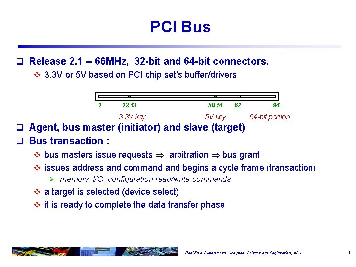
PCI Bus q Release 2. 1 -- 66 MHz, 32 -bit and 64 -bit connectors. v 3. 3 V or 5 V based on PCI chip set’s buffer/drivers 1 12, 13 3. 3 V key 50, 51 62 5 V key 94 64 -bit portion q Agent, bus master (initiator) and slave (target) q Bus transaction : v bus masters issue requests arbitration bus grant v issues address and command begins a cycle frame (transaction) Ø memory, I/O, configuration read/write commands v a target is selected (device select) v it is ready to complete the data transfer phase Real-time Systems Lab, Computer Science and Engineering, ASU 1

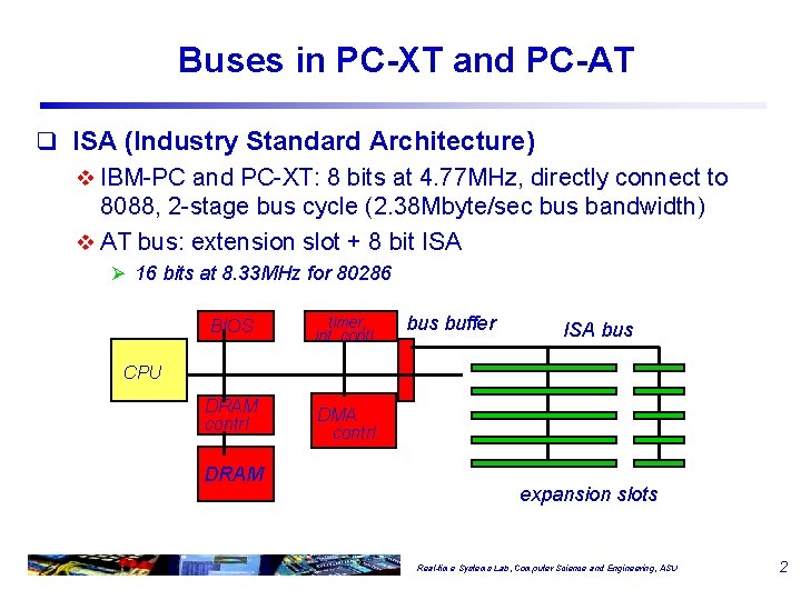
Buses in PC-XT and PC-AT q ISA (Industry Standard Architecture) v IBM-PC and PC-XT: 8 bits at 4. 77 MHz, directly connect to 8088, 2 -stage bus cycle (2. 38 Mbyte/sec bus bandwidth) v AT bus: extension slot + 8 bit ISA Ø 16 bits at 8. 33 MHz for 80286 BIOS timer, int. contl. bus buffer ISA bus CPU DRAM contrl. DRAM DMA contrl. expansion slots Real-time Systems Lab, Computer Science and Engineering, ASU 2

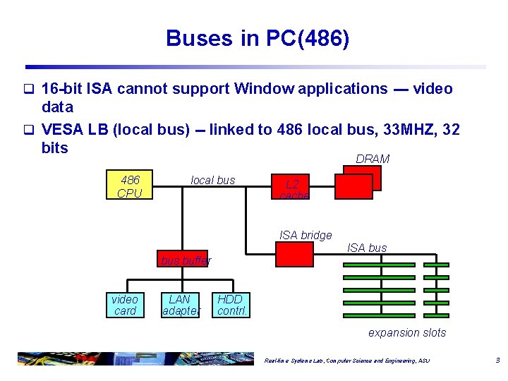
Buses in PC(486) q 16 -bit ISA cannot support Window applications --- video data q VESA LB (local bus) -- linked to 486 local bus, 33 MHZ, 32 bits DRAM 486 CPU local bus L 2 cache ISA bridge ISA bus buffer video card LAN adapter HDD contrl. expansion slots Real-time Systems Lab, Computer Science and Engineering, ASU 3

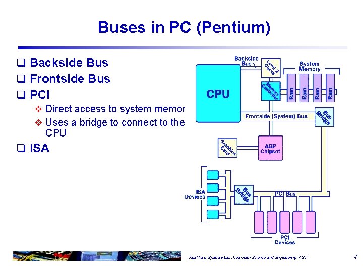
Buses in PC (Pentium) q Backside Bus q Frontside Bus q PCI v Direct access to system memory for connected devices v Uses a bridge to connect to the frontside bus and therefore to the CPU q ISA Real-time Systems Lab, Computer Science and Engineering, ASU 4

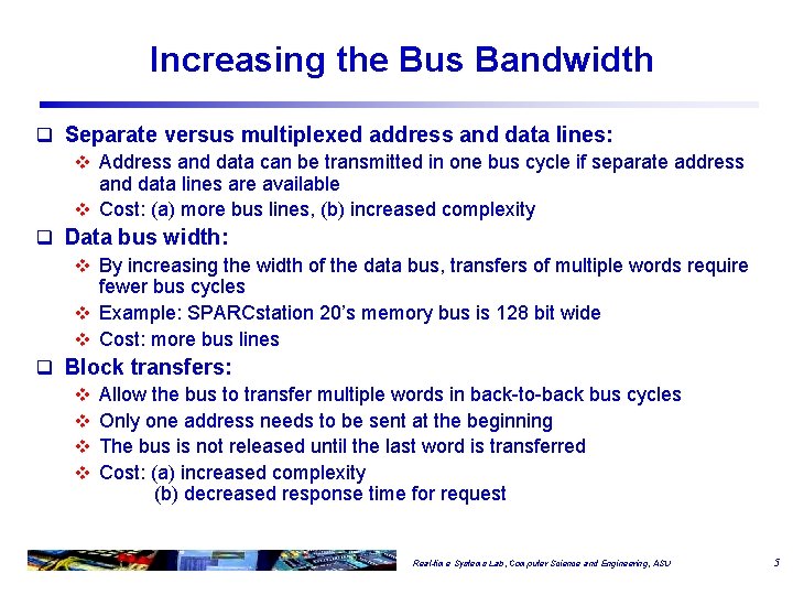
Increasing the Bus Bandwidth q Separate versus multiplexed address and data lines: v Address and data can be transmitted in one bus cycle if separate address and data lines are available v Cost: (a) more bus lines, (b) increased complexity q Data bus width: v By increasing the width of the data bus, transfers of multiple words require fewer bus cycles v Example: SPARCstation 20’s memory bus is 128 bit wide v Cost: more bus lines q Block transfers: v Allow the bus to transfer multiple words in back-to-back bus cycles v Only one address needs to be sent at the beginning v The bus is not released until the last word is transferred v Cost: (a) increased complexity (b) decreased response time for request Real-time Systems Lab, Computer Science and Engineering, ASU 5

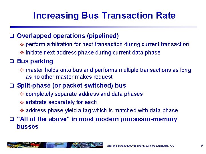
Increasing Bus Transaction Rate q Overlapped operations (pipelined) v perform arbitration for next transaction during current transaction v initiate next address phase during current data phase q Bus parking v master holds onto bus and performs multiple transactions as long as no other master makes request q Split-phase (or packet switched) bus v completely separate address and data phases v arbitrate separately for each v address phase yield a tag which is matched with data phase q ”All of the above” in most modern processor-memory busses Real-time Systems Lab, Computer Science and Engineering, ASU 6
![PCI Bus Signals PCI master device CLK AD63 32 CBE7 4 FRAME IRDY TRDY PCI Bus Signals PCI master device CLK AD[63: 32] C/BE[7: 4] FRAME IRDY TRDY](https://slidetodoc.com/presentation_image_h/832bce12cf78a0c82d24e325e95cf72d/image-8.jpg)
PCI Bus Signals PCI master device CLK AD[63: 32] C/BE[7: 4] FRAME IRDY TRDY REQ 64 ACK 64 DEVSEL STOP Misc control INT REQ C/BE[3: 0] AD[31: 0] A typical PCI read transaction BIST signals Error reporting REQ GNT RST Real-time Systems Lab, Computer Science and Engineering, ASU 7

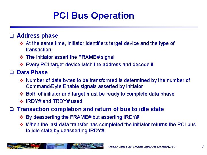
PCI Bus Operation q Address phase v At the same time, initiator identifiers target device and the type of transaction v The initiator assert the FRAME# signal v Every PCI target device latch the address and decode it q Data Phase v Number of data bytes to be transformed is determined by the number of Command/Byte Enable signals asserted by initiator v Both of initiator and target must be ready to complete data phase v IRDY# and TRDY# used q Transaction completion and return of bus to idle state v By deasserting the FRAME# but asserting IRDY# v When the last data transfer has completed the initiator returns the PCI bus to idle state by deasserting IRDY# Real-time Systems Lab, Computer Science and Engineering, ASU 8

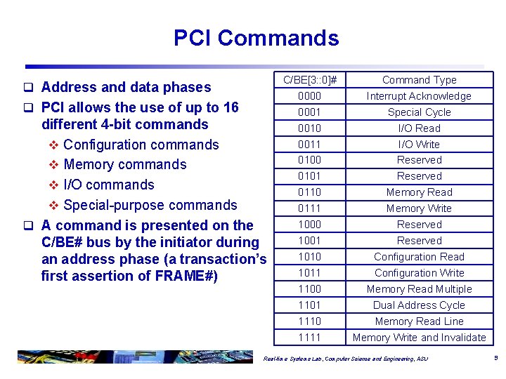
PCI Commands q Address and data phases q PCI allows the use of up to 16 different 4 -bit commands v Configuration commands v Memory commands v I/O commands v Special-purpose commands q A command is presented on the C/BE# bus by the initiator during an address phase (a transaction’s first assertion of FRAME#) C/BE[3: : 0]# Command Type 0000 Interrupt Acknowledge 0001 Special Cycle 0010 I/O Read 0011 I/O Write 0100 Reserved 0101 Reserved 0110 Memory Read 0111 Memory Write 1000 Reserved 1001 Reserved 1010 Configuration Read 1011 Configuration Write 1100 Memory Read Multiple 1101 Dual Address Cycle 1110 Memory Read Line 1111 Memory Write and Invalidate Real-time Systems Lab, Computer Science and Engineering, ASU 9

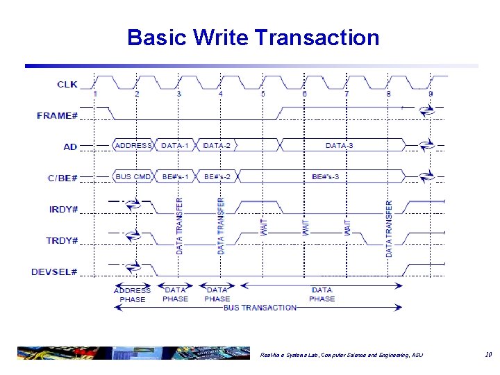
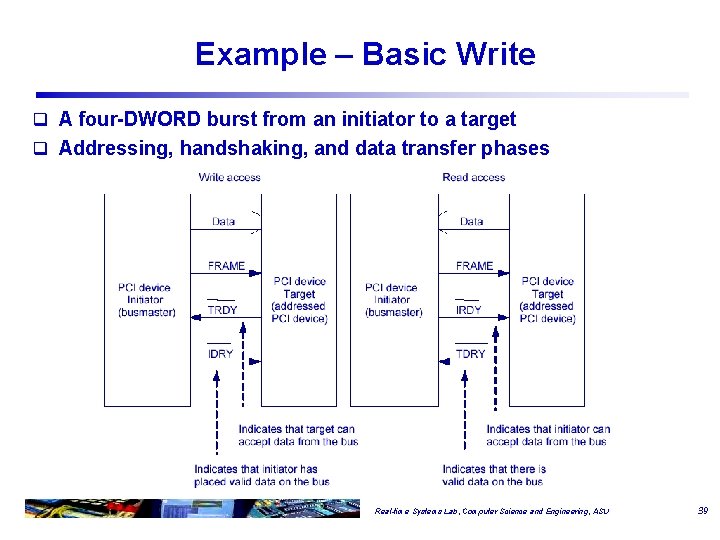
Basic Write Transaction Real-time Systems Lab, Computer Science and Engineering, ASU 10

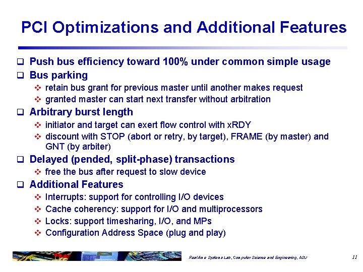
PCI Optimizations and Additional Features q Push bus efficiency toward 100% under common simple usage q Bus parking v retain bus grant for previous master until another makes request v granted master can start next transfer without arbitration q Arbitrary burst length v initiator and target can exert flow control with x. RDY v discount with STOP (abort or retry, by target), FRAME (by master) and GNT (by arbiter) q Delayed (pended, split-phase) transactions v free the bus after request to slow device q Additional Features v Interrupts: support for controlling I/O devices v Cache coherency: support for I/O and multiprocessors v Locks: support timesharing, I/O, and MPs v Configuration Address Space (plug and play) Real-time Systems Lab, Computer Science and Engineering, ASU 11

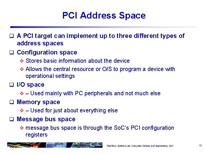
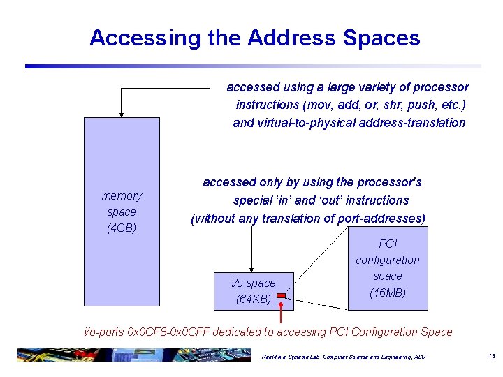
PCI Address Space q A PCI target can implement up to three different types of address spaces q Configuration space v Stores basic information about the device v Allows the central resource or O/S to program a device with operational settings q I/O space v – Used mainly with PC peripherals and not much else q Memory space v – Used for just about everything else q Message bus space v message bus space is through the So. C’s PCI configuration registers Real-time Systems Lab, Computer Science and Engineering, ASU 12

Accessing the Address Spaces accessed using a large variety of processor instructions (mov, add, or, shr, push, etc. ) and virtual-to-physical address-translation memory space (4 GB) accessed only by using the processor’s special ‘in’ and ‘out’ instructions (without any translation of port-addresses) i/o space (64 KB) PCI configuration space (16 MB) i/o-ports 0 x 0 CF 8 -0 x 0 CFF dedicated to accessing PCI Configuration Space Real-time Systems Lab, Computer Science and Engineering, ASU 13

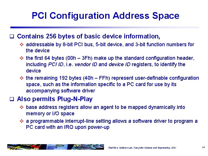
PCI Configuration Address Space q Contains 256 bytes of basic device information, v addressable by 8 -bit PCI bus, 5 -bit device, and 3 -bit function numbers for the device v the first 64 bytes (00 h – 3 Fh) make up the standard configuration header, including PCI ID, i. e. vendor ID and device ID registers, to identify the device v the remaining 192 bytes (40 h – FFh) represent user-definable configuration space, such as the information specific to a PC card for use by its accompanying software driver q Also permits Plug-N-Play v base address registers allow an agent to be mapped dynamically into memory or I/O space v a programmable interrupt-line setting allows a software driver to program a PC card with an IRQ upon power-up Real-time Systems Lab, Computer Science and Engineering, ASU 14

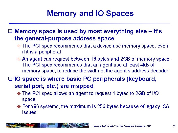
Memory and IO Spaces q Memory space is used by most everything else – it’s the general-purpose address space v The PCI spec recommends that a device use memory space, even if it is a peripheral v An agent can request between 16 bytes and 2 GB of memory space. The PCI spec recommends that an agent use at least 4 k. B of memory space, to reduce the width of the agent’s address decoder q IO space is where basic PC peripherals (keyboard, serial port, etc. ) are mapped v The PCI spec allows an agent to request 4 bytes to 2 GB of I/O space v For x 86 systems, the maximum is 256 bytes because of legacy ISA issues Real-time Systems Lab, Computer Science and Engineering, ASU 15

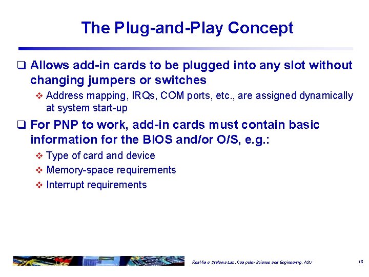
The Plug-and-Play Concept q Allows add-in cards to be plugged into any slot without changing jumpers or switches v Address mapping, IRQs, COM ports, etc. , are assigned dynamically at system start-up q For PNP to work, add-in cards must contain basic information for the BIOS and/or O/S, e. g. : v Type of card and device v Memory-space requirements v Interrupt requirements Real-time Systems Lab, Computer Science and Engineering, ASU 16

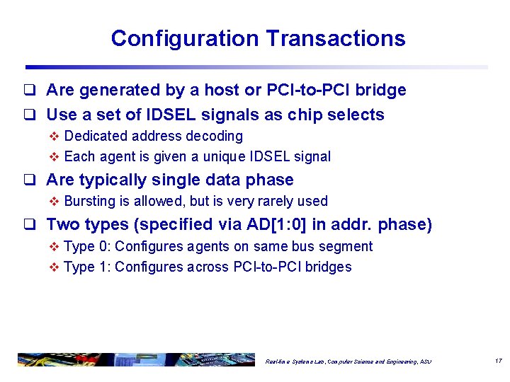
Configuration Transactions q Are generated by a host or PCI-to-PCI bridge q Use a set of IDSEL signals as chip selects v Dedicated address decoding v Each agent is given a unique IDSEL signal q Are typically single data phase v Bursting is allowed, but is very rarely used q Two types (specified via AD[1: 0] in addr. phase) v Type 0: Configures agents on same bus segment v Type 1: Configures across PCI-to-PCI bridges Real-time Systems Lab, Computer Science and Engineering, ASU 17

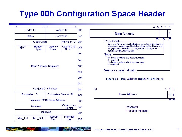
Type 00 h Configuration Space Header Real-time Systems Lab, Computer Science and Engineering, ASU 18

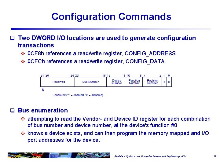
Configuration Commands q Two DWORD I/O locations are used to generate configuration transactions v 0 CF 8 h references a read/write register, CONFIG_ADDRESS. v 0 CFCh references a read/write register, CONFIG_DATA. q Bus enumeration v attempting to read the Vendor- and Device ID register for each combination of bus number and device number, at the device's function #0 v knows a device exists, and can then program the memory mapped and I/O port addresses for the device. Real-time Systems Lab, Computer Science and Engineering, ASU 19

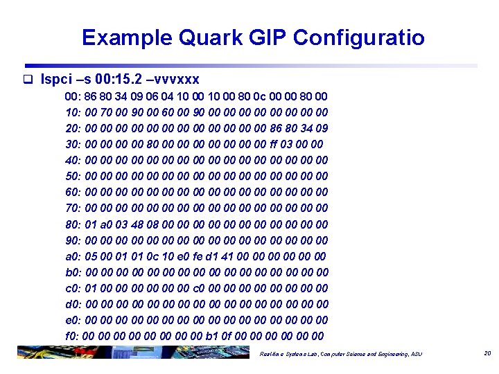
Example Quark GIP Configuratio q lspci –s 00: 15. 2 –vvvxxx 00: 86 80 34 09 06 04 10 00 80 0 c 00 00 80 00 10: 00 70 00 90 00 60 00 90 00 00 20: 00 00 00 86 80 34 09 30: 00 00 80 00 00 ff 03 00 00 40: 00 00 00 00 50: 00 00 00 00 60: 00 00 00 00 70: 00 00 00 00 80: 01 a 0 03 48 08 00 00 00 90: 00 00 00 00 a 0: 05 00 01 01 0 c 10 e 0 fe d 1 41 00 00 00 b 0: 00 00 00 00 c 0: 01 00 00 00 c 0 00 00 d 0: 00 00 00 00 e 0: 00 00 00 00 f 0: 00 00 b 1 0 f 00 00 00 Real-time Systems Lab, Computer Science and Engineering, ASU 20

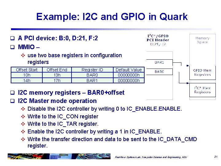
Example: I 2 C and GPIO in Quark q A PCI device: B: 0, D: 21, F: 2 q MMIO – v use two base registers in configuration registers Offset Start 10 h 14 h Offset End 13 h 17 h Register ID BAR 0 BAR 1 Default Value 00000000 h q I 2 C memory registers – BAR 0+offset q I 2 C Master mode operation v Disable the I 2 C controller by writing 0 to IC_ENABLE. v Write to the IC_CON register v Write to the IC_TAR register. v Enable the I 2 C controller by writing a 1 in IC_ENABLE. v Write the transfer direction and data to be sent to the IC_DATA_CMD register. Real-time Systems Lab, Computer Science and Engineering, ASU 21

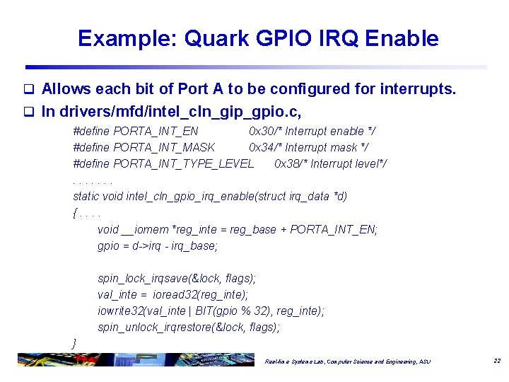
Example: Quark GPIO IRQ Enable q Allows each bit of Port A to be configured for interrupts. q In drivers/mfd/intel_cln_gip_gpio. c, #define PORTA_INT_EN 0 x 30/* Interrupt enable */ #define PORTA_INT_MASK 0 x 34/* Interrupt mask */ #define PORTA_INT_TYPE_LEVEL 0 x 38/* Interrupt level*/. . . . static void intel_cln_gpio_irq_enable(struct irq_data *d) {. . void __iomem *reg_inte = reg_base + PORTA_INT_EN; gpio = d->irq - irq_base; spin_lock_irqsave(&lock, flags); val_inte = ioread 32(reg_inte); iowrite 32(val_inte | BIT(gpio % 32), reg_inte); spin_unlock_irqrestore(&lock, flags); } Real-time Systems Lab, Computer Science and Engineering, ASU 22

PCI Challenges q Limited Bandwidth v PCI-X and Advanced Graphics Port (AGP) for higher frequency v Reduction of distance q Bandwidth shared between all devices q Limited host pin-count q Lack of support for real time data transfer q Stringent routing rules q Lack of scaling with frequency and voltage q Absence of power management q PCI-X -- an enhancement of the 32 -bit PCI Local Bus for a higher bandwidth demand. v a double-wide version of PCI, running at up to four times the clock speed Real-time Systems Lab, Computer Science and Engineering, ASU 23

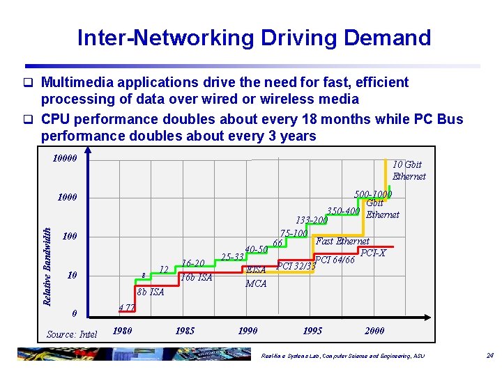
Inter-Networking Driving Demand q Multimedia applications drive the need for fast, efficient processing of data over wired or wireless media q CPU performance doubles about every 18 months while PC Bus performance doubles about every 3 years 10000 10 Gbit Ethernet Relative Bandwidth 1000 10 8 12 8 b ISA 0 Source: Intel 500 -1000 Gbit 350 -400 Ethernet 133 -200 75 -100 Fast Ethernet 66 40 -50 PCI-X 25 -33 PCI 64/66 16 -20 EISA PCI 32/33 16 b ISA MCA 4. 77 1980 1985 1990 1995 2000 Real-time Systems Lab, Computer Science and Engineering, ASU 24

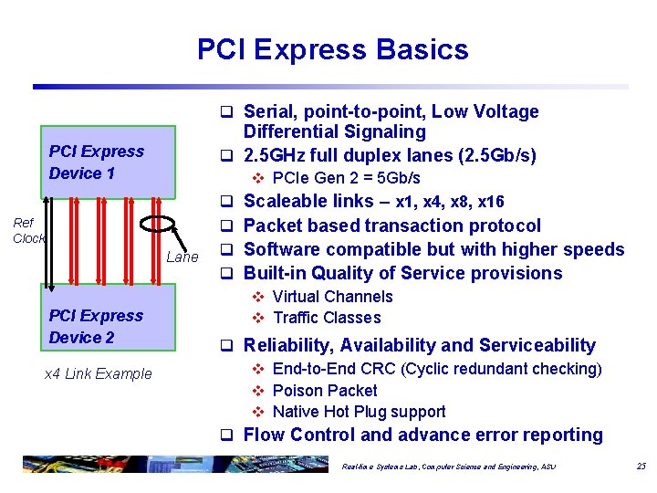
PCI Express Basics q Serial, point-to-point, Low Voltage Differential Signaling q 2. 5 GHz full duplex lanes (2. 5 Gb/s) PCI Express Device 1 v PCIe Gen 2 = 5 Gb/s Ref Clock Lane PCI Express Device 2 x 4 Link Example q q Scaleable links – x 1, x 4, x 8, x 16 Packet based transaction protocol Software compatible but with higher speeds Built-in Quality of Service provisions v Virtual Channels v Traffic Classes q Reliability, Availability and Serviceability v End-to-End CRC (Cyclic redundant checking) v Poison Packet v Native Hot Plug support q Flow Control and advance error reporting Real-time Systems Lab, Computer Science and Engineering, ASU 25

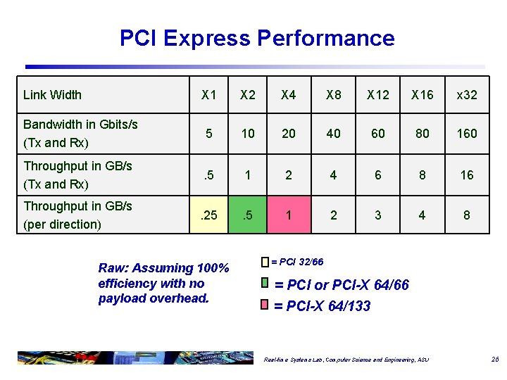
PCI Express Performance Link Width X 1 X 2 X 4 X 8 X 12 X 16 x 32 Bandwidth in Gbits/s (Tx and Rx) 5 10 20 40 60 80 160 Throughput in GB/s (Tx and Rx) . 5 1 2 4 6 8 16 Throughput in GB/s (per direction) . 25 . 5 1 2 3 4 8 Raw: Assuming 100% efficiency with no payload overhead. = PCI 32/66 = PCI or PCI-X 64/66 = PCI-X 64/133 Real-time Systems Lab, Computer Science and Engineering, ASU 26

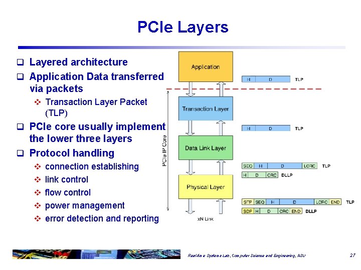
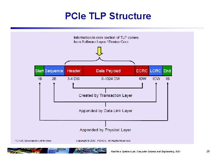
PCIe Layers q Layered architecture q Application Data transferred via packets v Transaction Layer Packet (TLP) q PCIe core usually implement the lower three layers q Protocol handling v connection establishing v link control v flow control v power management v error detection and reporting Real-time Systems Lab, Computer Science and Engineering, ASU 27

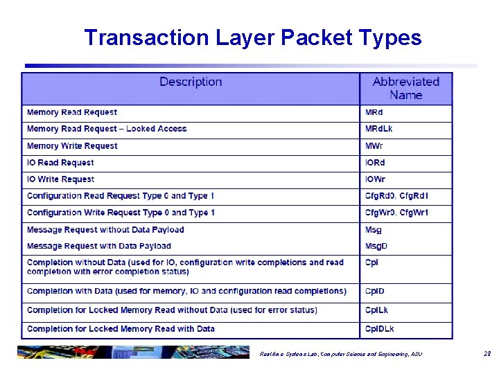
Transaction Layer Packet Types Real-time Systems Lab, Computer Science and Engineering, ASU 28

PCIe TLP Structure Real-time Systems Lab, Computer Science and Engineering, ASU 29

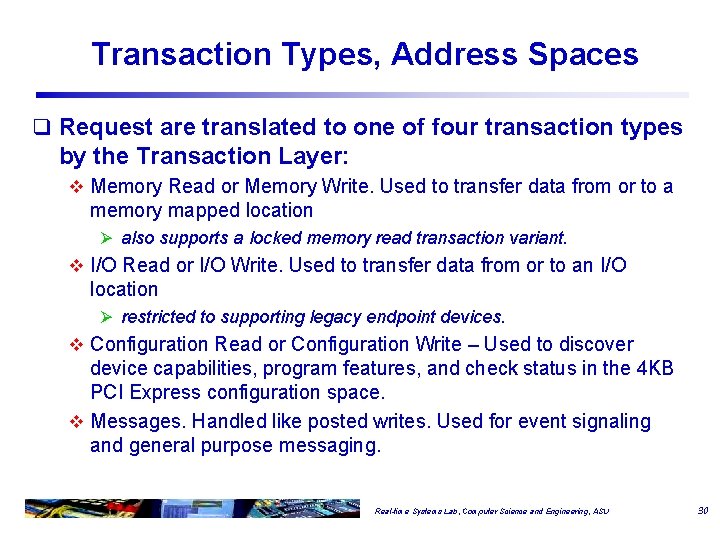
Transaction Types, Address Spaces q Request are translated to one of four transaction types by the Transaction Layer: v Memory Read or Memory Write. Used to transfer data from or to a memory mapped location Ø also supports a locked memory read transaction variant. v I/O Read or I/O Write. Used to transfer data from or to an I/O location Ø restricted to supporting legacy endpoint devices. v Configuration Read or Configuration Write – Used to discover device capabilities, program features, and check status in the 4 KB PCI Express configuration space. v Messages. Handled like posted writes. Used for event signaling and general purpose messaging. Real-time Systems Lab, Computer Science and Engineering, ASU 30

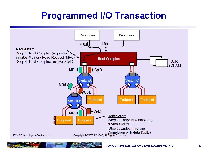
Programmed I/O Transaction Real-time Systems Lab, Computer Science and Engineering, ASU 31

Back-up Slides Real-time Systems Lab, Computer Science and Engineering, ASU 32

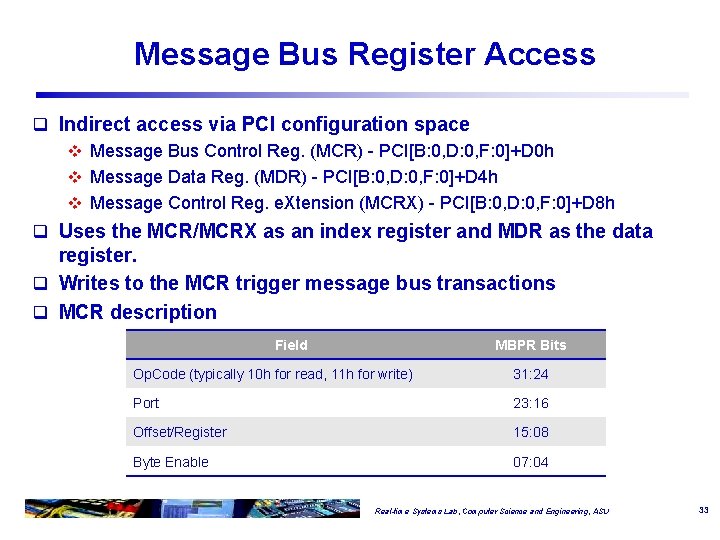
Message Bus Register Access q Indirect access via PCI configuration space v Message Bus Control Reg. (MCR) - PCI[B: 0, D: 0, F: 0]+D 0 h v Message Data Reg. (MDR) - PCI[B: 0, D: 0, F: 0]+D 4 h v Message Control Reg. e. Xtension (MCRX) - PCI[B: 0, D: 0, F: 0]+D 8 h q Uses the MCR/MCRX as an index register and MDR as the data register. q Writes to the MCR trigger message bus transactions q MCR description Field MBPR Bits Op. Code (typically 10 h for read, 11 h for write) 31: 24 Port 23: 16 Offset/Register 15: 08 Byte Enable 07: 04 Real-time Systems Lab, Computer Science and Engineering, ASU 33

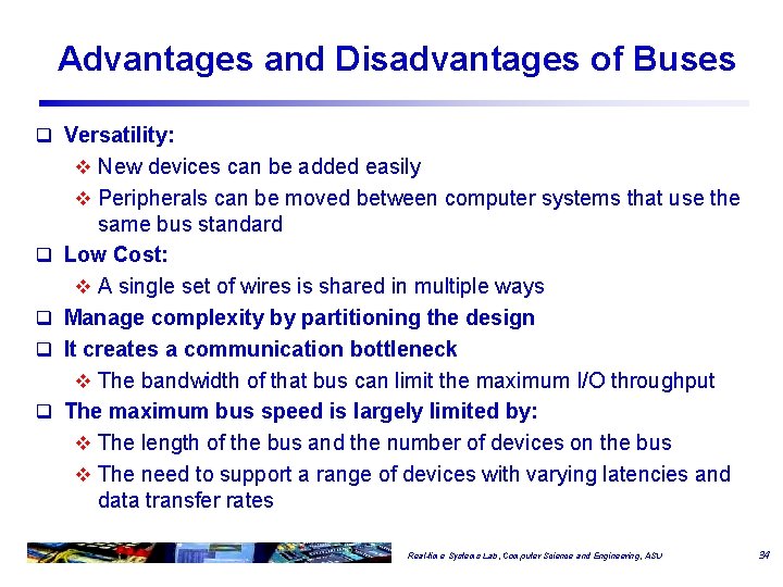
Advantages and Disadvantages of Buses q Versatility: v New devices can be added easily v Peripherals can be moved between computer systems that use the q q same bus standard Low Cost: v A single set of wires is shared in multiple ways Manage complexity by partitioning the design It creates a communication bottleneck v The bandwidth of that bus can limit the maximum I/O throughput The maximum bus speed is largely limited by: v The length of the bus and the number of devices on the bus v The need to support a range of devices with varying latencies and data transfer rates Real-time Systems Lab, Computer Science and Engineering, ASU 34

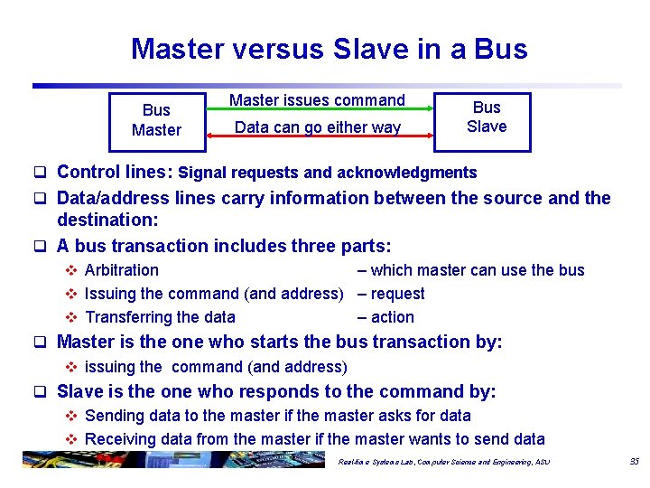
Master versus Slave in a Bus Master issues command Data can go either way Bus Slave q Control lines: Signal requests and acknowledgments q Data/address lines carry information between the source and the destination: q A bus transaction includes three parts: v Arbitration – which master can use the bus v Issuing the command (and address) – request v Transferring the data – action q Master is the one who starts the bus transaction by: v issuing the command (and address) q Slave is the one who responds to the command by: v Sending data to the master if the master asks for data v Receiving data from the master if the master wants to send data Real-time Systems Lab, Computer Science and Engineering, ASU 35

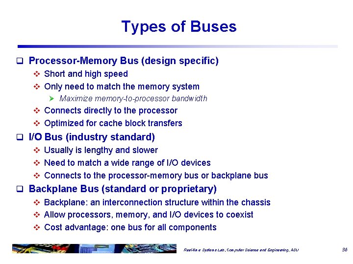
Types of Buses q Processor-Memory Bus (design specific) v Short and high speed v Only need to match the memory system Ø Maximize memory-to-processor bandwidth v Connects directly to the processor v Optimized for cache block transfers q I/O Bus (industry standard) v Usually is lengthy and slower v Need to match a wide range of I/O devices v Connects to the processor-memory bus or backplane bus q Backplane Bus (standard or proprietary) v Backplane: an interconnection structure within the chassis v Allow processors, memory, and I/O devices to coexist v Cost advantage: one bus for all components Real-time Systems Lab, Computer Science and Engineering, ASU 36

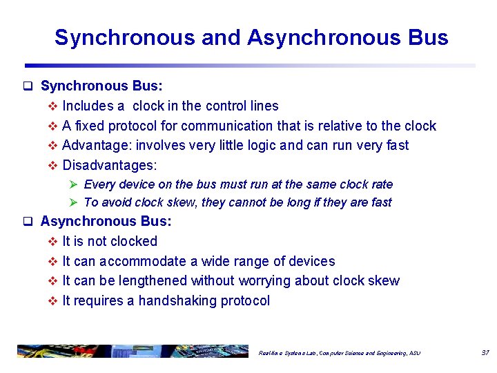
Synchronous and Asynchronous Bus q Synchronous Bus: v Includes a clock in the control lines v A fixed protocol for communication that is relative to the clock v Advantage: involves very little logic and can run very fast v Disadvantages: Ø Every device on the bus must run at the same clock rate Ø To avoid clock skew, they cannot be long if they are fast q Asynchronous Bus: v It is not clocked v It can accommodate a wide range of devices v It can be lengthened without worrying about clock skew v It requires a handshaking protocol Real-time Systems Lab, Computer Science and Engineering, ASU 37

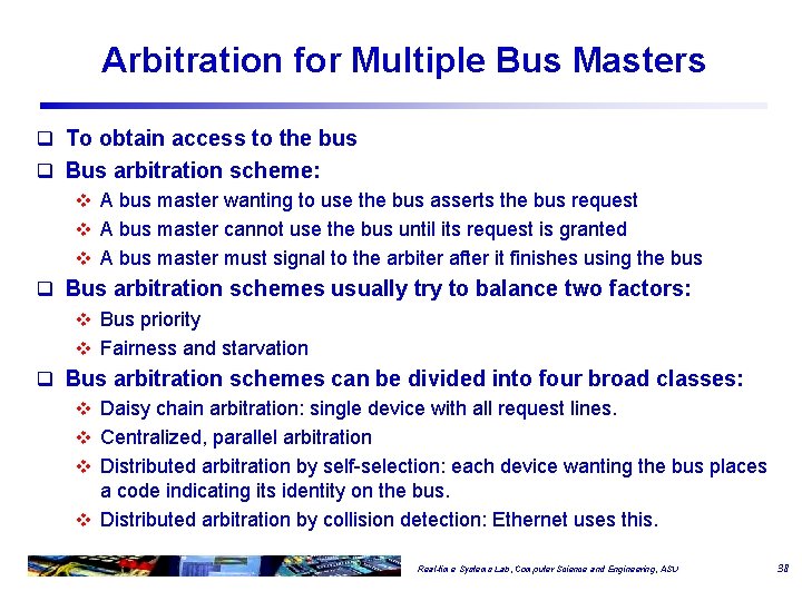
Arbitration for Multiple Bus Masters q To obtain access to the bus q Bus arbitration scheme: v A bus master wanting to use the bus asserts the bus request v A bus master cannot use the bus until its request is granted v A bus master must signal to the arbiter after it finishes using the bus q Bus arbitration schemes usually try to balance two factors: v Bus priority v Fairness and starvation q Bus arbitration schemes can be divided into four broad classes: v Daisy chain arbitration: single device with all request lines. v Centralized, parallel arbitration v Distributed arbitration by self-selection: each device wanting the bus places a code indicating its identity on the bus. v Distributed arbitration by collision detection: Ethernet uses this. Real-time Systems Lab, Computer Science and Engineering, ASU 38

Example – Basic Write q A four-DWORD burst from an initiator to a target q Addressing, handshaking, and data transfer phases Real-time Systems Lab, Computer Science and Engineering, ASU 39

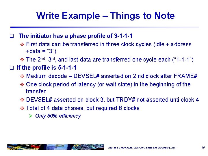
Write Example – Things to Note q The initiator has a phase profile of 3 -1 -1 -1 v First data can be transferred in three clock cycles (idle + address +data = “ 3”) v The 2 nd, 3 rd, and last data are transferred one cycle each (“ 1 -1 -1”) q If the profile is 5 -1 -1 -1 v Medium decode – DEVSEL# asserted on 2 nd clock after FRAME# v One clock period of latency (or wait state) in the beginning of the transfer v DEVSEL# asserted on clock 3, but TRDY# not asserted unti clock 4 v Total of 4 data phases, but required 8 clocks Ø Only 50% efficiency Real-time Systems Lab, Computer Science and Engineering, ASU 40

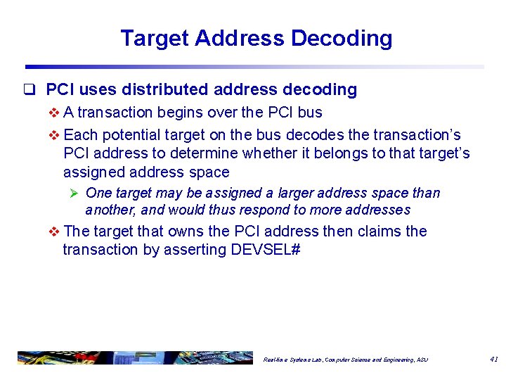
Target Address Decoding q PCI uses distributed address decoding v A transaction begins over the PCI bus v Each potential target on the bus decodes the transaction’s PCI address to determine whether it belongs to that target’s assigned address space Ø One target may be assigned a larger address space than another, and would thus respond to more addresses v The target that owns the PCI address then claims the transaction by asserting DEVSEL# Real-time Systems Lab, Computer Science and Engineering, ASU 41

More Terms q Turnaround cycle v “Dead” bus cycle to prevent bus contention q Wait state v A bus cycle where it is possible to transfer data, but no data transfer occurs v Wait states may be inserted dynamically by the initiator or target Ø Target deasserts TRDY# to signal it is not ready Ø Initiator deasserts IRDY# to signal it is not ready q Target termination v Either agent may signal the end of a transaction Ø The target signals termination by asserting STOP# Ø The initiator signals completion by deasserting FRAME# Real-time Systems Lab, Computer Science and Engineering, ASU 42

Zero and One Wait State q A one-wait-state agent inserts a wait state at the beginning of each data phase v This is done if an agent – built in older, slower silicon – needs to pipeline critical paths internally v Reduces bandwidth by 50% q The need to insert a wait state is typically an issue only when the agent is sourcing data (initiator write or target read) v This is because such an agent would have to sample its counterpart’s x. RDY# signal to see if that agent accepted data, then fan out to 36 or more clock enables (for AD[31: 0] and possibly C/BE#[3: 0]) to drive the next piece of data onto the PCI bus. . . all within 11 ns! Real-time Systems Lab, Computer Science and Engineering, ASU 43