
PCB Design for Accurate Gauging Assuring Accuracy and

PCB Design for Accurate Gauging Assuring Accuracy and Improving EMI and ESD Performance Thomas Cosby Applications Engineer 24 October 2012
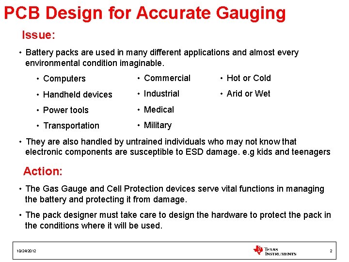
PCB Design for Accurate Gauging Issue: • Battery packs are used in many different applications and almost every environmental condition imaginable. • Computers • Commercial • Hot or Cold • Handheld devices • Industrial • Arid or Wet • Power tools • Medical • Transportation • Military • They are also handled by untrained individuals who may not know that electronic components are susceptible to ESD damage. e. g kids and teenagers Action: • The Gas Gauge and Cell Protection devices serve vital functions in managing the battery and protecting it from damage. • The pack designer must take care to design the hardware to protect the pack in the conditions where it will be used. 10/24/2012 2

Assuring Accuracy 10/24/2012 3
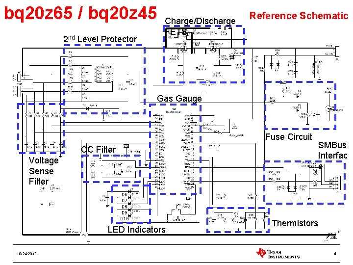
bq 20 z 65 / bq 20 z 45 2 nd Level Protector Charge/Discharge FETS Reference Schematic Gas Gauge Fuse Circuit CC Filter Voltage Sense Filter LED Indicators SMBus Interfac e Thermistors 4 10/24/2012 4
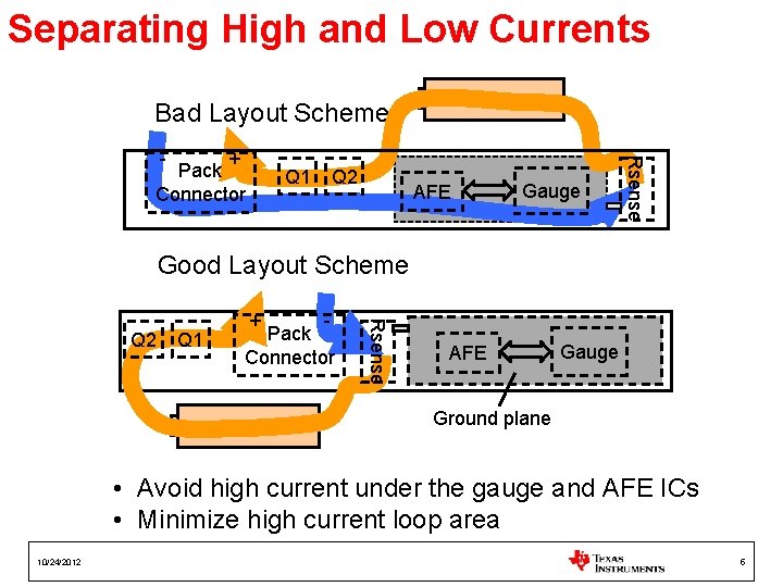
Separating High and Low Currents Bad Layout Scheme + Pack Connector Q 1 Q 2 AFE Gauge Rsense - Good Layout Scheme Q 1 Pack Connector Rsense Q 2 + AFE Gauge Ground plane • Avoid high current under the gauge and AFE ICs • Minimize high current loop area 10/24/2012 5
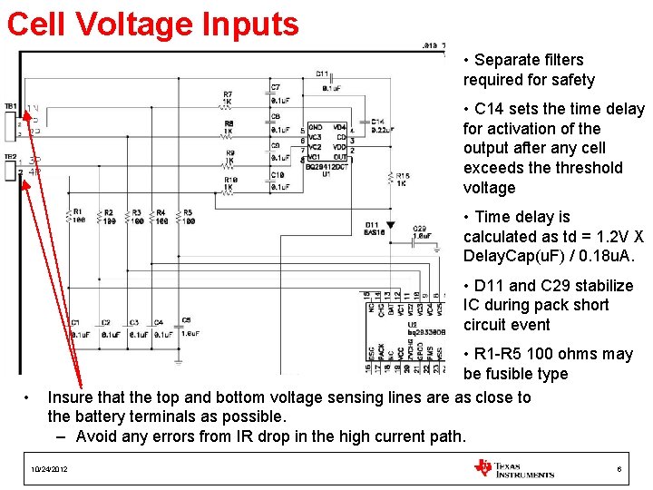
Cell Voltage Inputs • Separate filters required for safety • C 14 sets the time delay for activation of the output after any cell exceeds the threshold voltage • Time delay is calculated as td = 1. 2 V X Delay. Cap(u. F) / 0. 18 u. A. • D 11 and C 29 stabilize IC during pack short circuit event • • R 1 -R 5 100 ohms may be fusible type Insure that the top and bottom voltage sensing lines are as close to the battery terminals as possible. – Avoid any errors from IR drop in the high current path. 10/24/2012 6
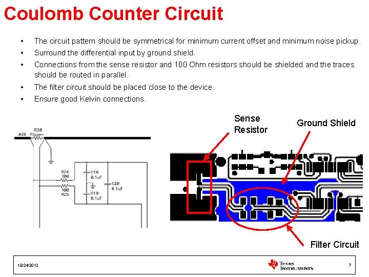
Coulomb Counter Circuit • The circuit pattern should be symmetrical for minimum current offset and minimum noise pickup. • Surround the differential input by ground shield. • Connections from the sense resistor and 100 Ohm resistors should be shielded and the traces should be routed in parallel. • The filter circuit should be placed close to the device. • Ensure good Kelvin connections. Sense Resistor Ground Shield Filter Circuit 10/24/2012 7
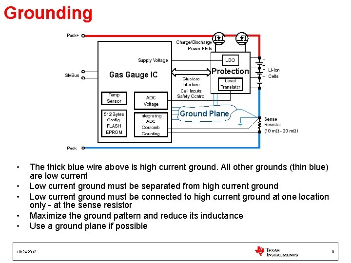
Grounding • • • The thick blue wire above is high current ground. All other grounds (thin blue) are low current Low current ground must be separated from high current ground Low current ground must be connected to high current ground at one location only - at the sense resistor Maximize the ground pattern and reduce its inductance Use a ground plane if possible 10/24/2012 8
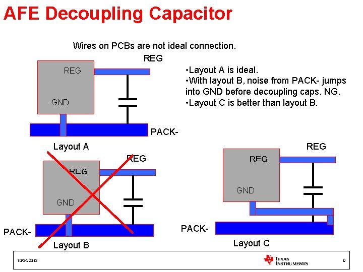
AFE Decoupling Capacitor Wires on PCBs are not ideal connection. REG • Layout A is ideal. REG • With layout B, noise from PACK- jumps into GND before decoupling caps. NG. GND • Layout C is better than layout B. PACKREG Layout A REG REG GND PACK- PACKLayout B 10/24/2012 Layout C 9

ESD Protection 10/24/2012 10
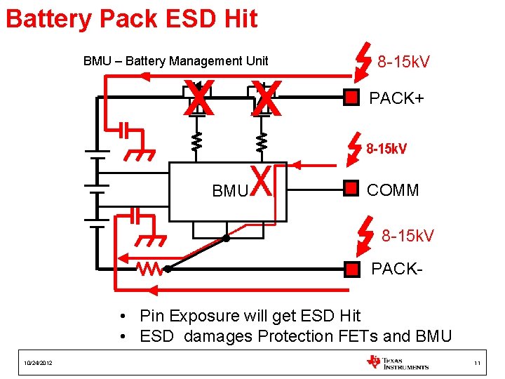
Battery Pack ESD Hit BMU – Battery Management Unit 8 -15 k. V x x PACK+ BMU COMM 8 -15 k. V PACK- • Pin Exposure will get ESD Hit • ESD damages Protection FETs and BMU 10/24/2012 11
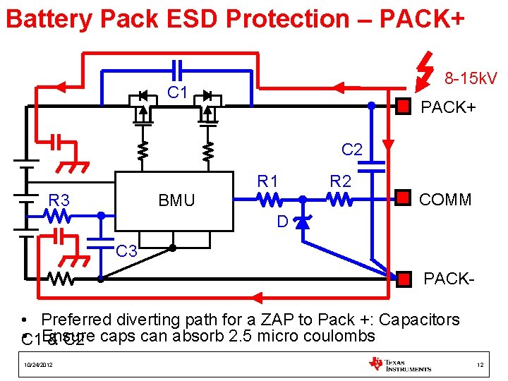
Battery Pack ESD Protection – PACK+ 8 -15 k. V C 1 PACK+ C 2 R 3 BMU R 1 R 2 COMM D C 3 PACK- • Preferred diverting path for a ZAP to Pack +: Capacitors • Ensure C 1 & C 2 caps can absorb 2. 5 micro coulombs 10/24/2012 12
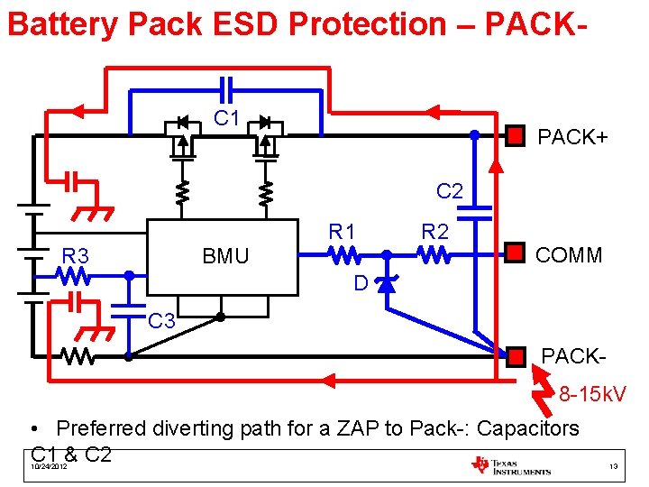
Battery Pack ESD Protection – PACKC 1 PACK+ C 2 R 3 BMU R 1 R 2 COMM D C 3 PACK 8 -15 k. V • Preferred diverting path for a ZAP to Pack-: Capacitors C 1 & C 2 10/24/2012 13
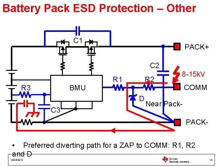
Battery Pack ESD Protection – Other C 1 PACK+ C 2 R 3 BMU R 1 R 2 D C 3 8 -15 k. V COMM Near Pack. PACK- • Preferred diverting path for a ZAP to COMM: R 1, R 2 and D 10/24/2012 14
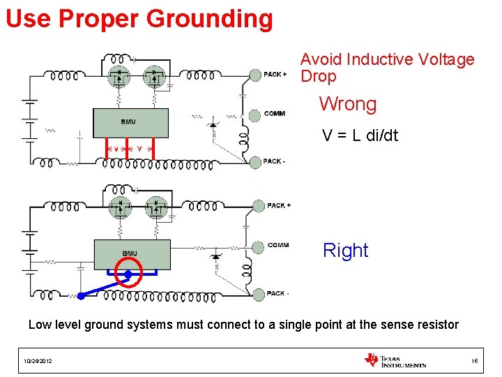
Use Proper Grounding Avoid Inductive Voltage Drop Wrong V = L di/dt Right Low level ground systems must connect to a single point at the sense resistor 10/24/2012 15
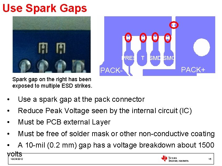
Use Spark Gaps PRES T SMD SMC PACK- PACK+ Spark gap on the right has been exposed to multiple ESD strikes. • Use a spark gap at the pack connector • Reduce Peak Voltage seen by the internal circuit (IC) • Must be PCB external Layer • Must be free of solder mask or other non-conductive coating • A 10 -mil (0. 2 mm) gap has a voltage breakdown about 1500 volts 10/24/2012 16
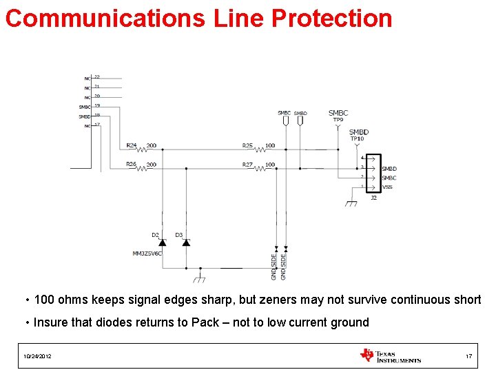
Communications Line Protection • 100 ohms keeps signal edges sharp, but zeners may not survive continuous short • Insure that diodes returns to Pack – not to low current ground 10/24/2012 17
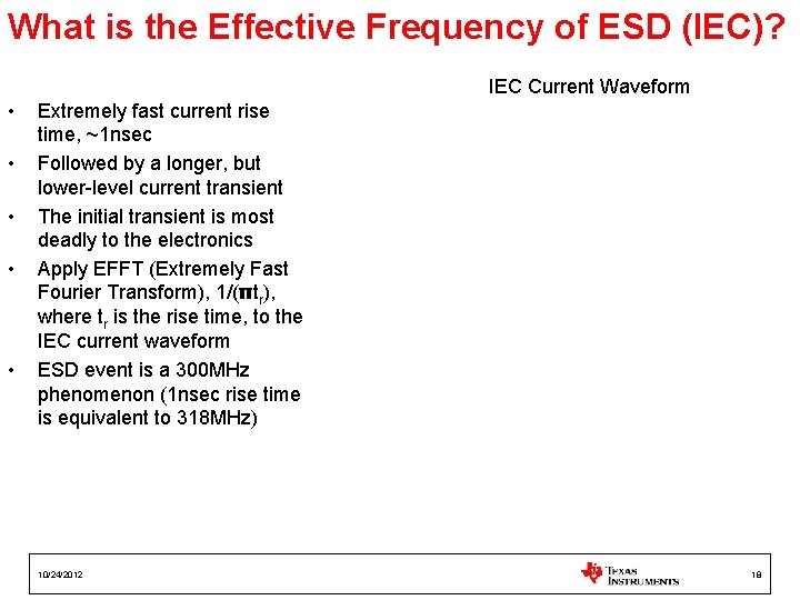
What is the Effective Frequency of ESD (IEC)? IEC Current Waveform • • • Extremely fast current rise time, ~1 nsec Followed by a longer, but lower-level current transient The initial transient is most deadly to the electronics Apply EFFT (Extremely Fast Fourier Transform), 1/(πtr), where tr is the rise time, to the IEC current waveform ESD event is a 300 MHz phenomenon (1 nsec rise time is equivalent to 318 MHz) 10/24/2012 18
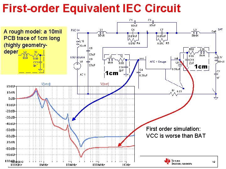
First-order Equivalent IEC Circuit A rough model: a 10 mil PCB trace of 1 cm long (highly geometrydependent!) 1 cm First order simulation: VCC is worse than BAT 6/5/2021 10/24/2012 "TI Proprietary Information" 19

Effects of PCB Trace Length Minimize trace lengths VCC Trace length: 1 cm 5 cm 10 cm IEC frequency resonances 6/5/2021 10/24/2012 "TI Proprietary Information" 20
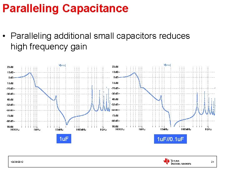
Paralleling Capacitance • Paralleling additional small capacitors reduces high frequency gain 1 u. F 10/24/2012 1 u. F//0. 1 u. F 21
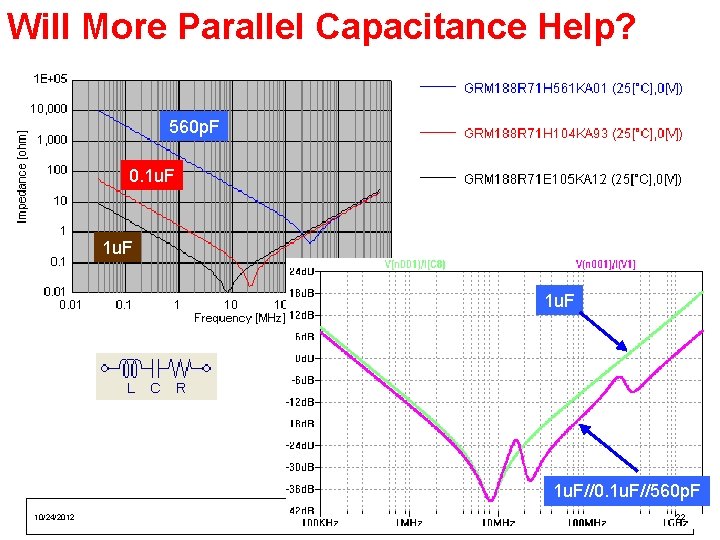
Will More Parallel Capacitance Help? 560 p. F 0. 1 u. F "TI Proprietary Information" 10/24/2012 1 u. F//0. 1 u. F//560 p. F 22
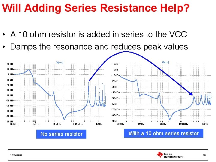
Will Adding Series Resistance Help? • A 10 ohm resistor is added in series to the VCC • Damps the resonance and reduces peak values No series resistor 10/24/2012 With a 10 ohm series resistor 23

EMI Protection 10/24/2012 24
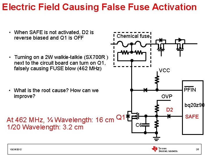
Electric Field Causing False Fuse Activation • When SAFE is not activated, D 2 is reverse biased and Q 1 is OFF Chemical fuse • Turning on a 2 W walkie-talkie (SX 700 R ) next to the circuit board can turn on Q 1, falsely causing FUSE blow (462 MHz) VCC PFIN • What is the root cause? How can we improve? OVP D 2 At 462 MHz, ¼ Wavelength: 16 cm Q 1 1/20 Wavelength: 3. 2 cm 10/24/2012 bq 20 z 90 SAFE C 6 25
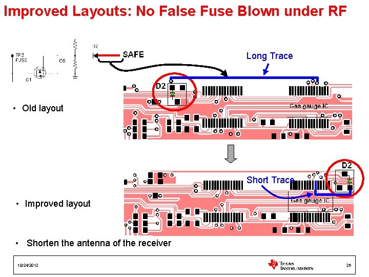
Improved Layouts: No False Fuse Blown under RF Long Trace • Old layout Short Trace • Improved layout • Shorten the antenna of the receiver 10/24/2012 26
Common Mode Issues • 90% of EMI problems are caused by CM Current spreading to areas where it can couple into something which can Resonate and Radiate. • All CM current comes from Intended Fields which are NOT properly contained!! • “Ground” is often considered a region of zero voltage potential with zero resistance or impedance, but this is not true except at DC. 10/24/2012 27
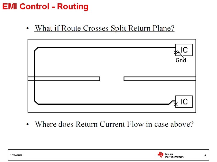
EMI Control - Routing 10/24/2012 28
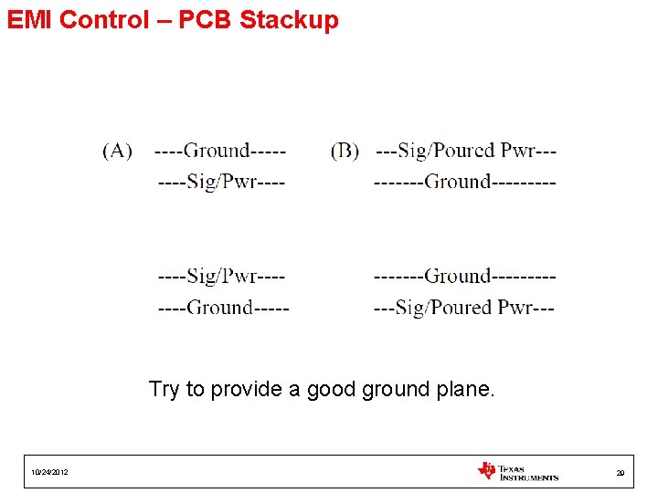
EMI Control – PCB Stackup Try to provide a good ground plane. 10/24/2012 29

bq 40 z 50 Next Generation IT Battery Manager 10/24/2012 30
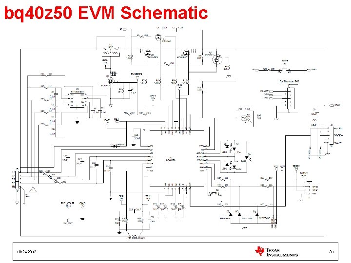
bq 40 z 50 EVM Schematic 10/24/2012 31

bq 40 z 50 EVM Layout Signal Plane GND Plane Gas Gauge High Temp Section Power Stage Cell Inputs Top Layer 10/24/2012 2 nd Layer 3 rd Layer Bottom Layer 32
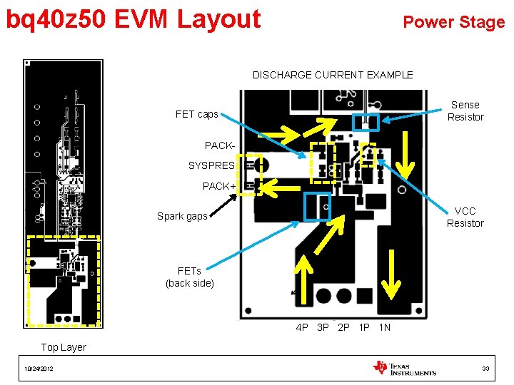
bq 40 z 50 EVM Layout Power Stage DISCHARGE CURRENT EXAMPLE Sense Resistor FET caps PACKSYSPRES PACK+ VCC Resistor Spark gaps FETs (back side) 4 P 3 P 2 P 1 P 1 N Top Layer 10/24/2012 33
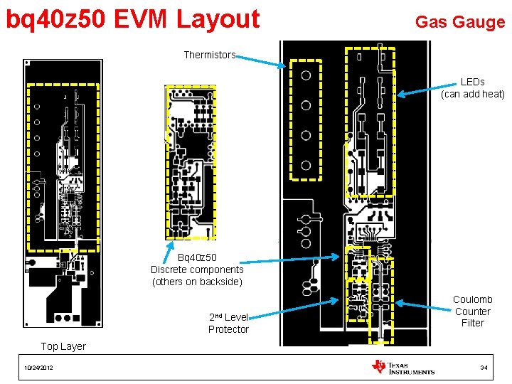
bq 40 z 50 EVM Layout Gas Gauge Thermistors LEDs (can add heat) Bq 40 z 50 Discrete components (others on backside) 2 nd Level Protector Coulomb Counter Filter Top Layer 10/24/2012 34
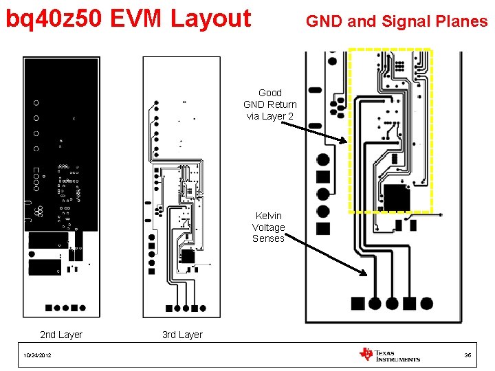
bq 40 z 50 EVM Layout GND and Signal Planes Good GND Return via Layer 2 Kelvin Voltage Senses 2 nd Layer 10/24/2012 3 rd Layer 35

Questions 6/5/2021 TI Confidential - NDA Restrictions 36
- Slides: 36