Pass Transistor and Dynamic Logic 1 2 to


- Slides: 34

Pass Transistor and Dynamic Logic 1

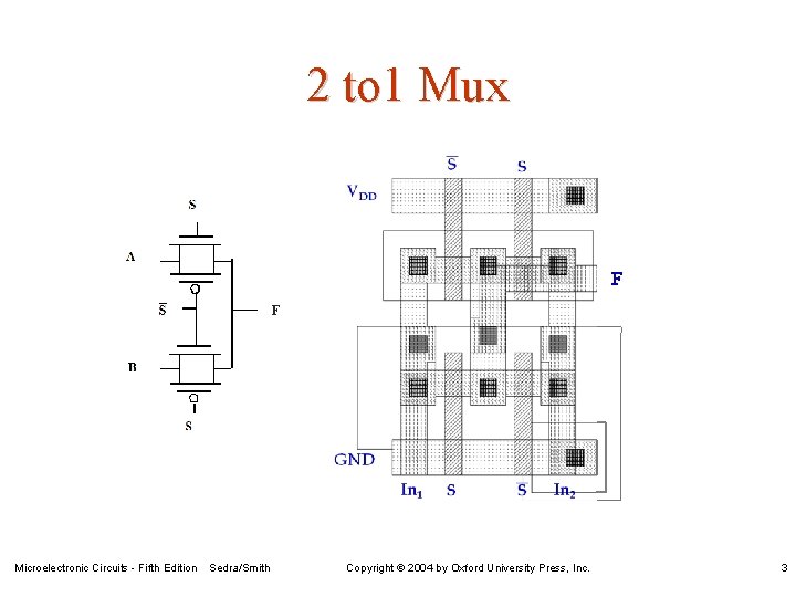
2 to 1 Mux How is the 2 to 1 Mux in CMOS Complementary Logic ? Microelectronic Circuits - Fifth Edition Sedra/Smith Copyright 2004 by Oxford University Press, Inc. 2

2 to 1 Mux F F Microelectronic Circuits - Fifth Edition Sedra/Smith Copyright 2004 by Oxford University Press, Inc. 3

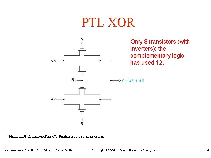
PTL XOR Only 8 transistors (with inverters); the complementary logic has used 12. Figure 10. 31 Realization of the XOR function using pass-transistor logic. Microelectronic Circuits - Fifth Edition Sedra/Smith Copyright 2004 by Oxford University Press, Inc. 4

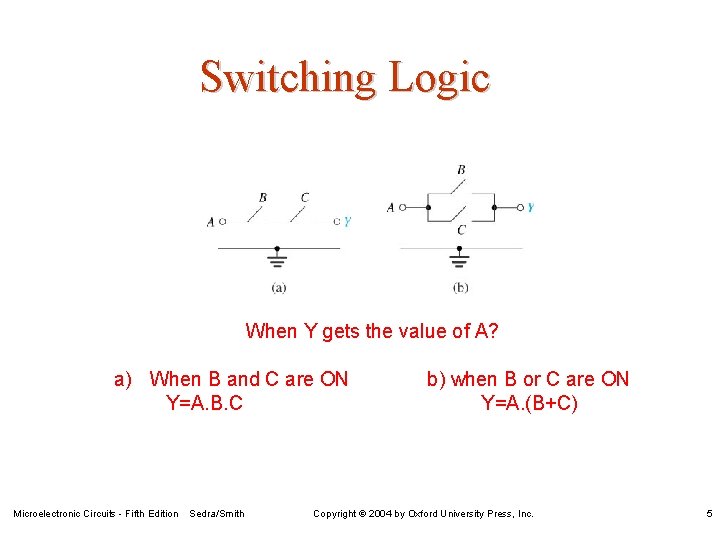
Switching Logic When Y gets the value of A? a) When B and C are ON Y=A. B. C Microelectronic Circuits - Fifth Edition Sedra/Smith b) when B or C are ON Y=A. (B+C) Copyright 2004 by Oxford University Press, Inc. 5

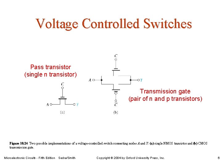
Voltage Controlled Switches Pass transistor (single n transistor) Transmission gate (pair of n and p transistors) Figure 10. 24 Two possible implementations of a voltage-controlled switch connecting nodes A and Y: (a) single NMOS transistor and (b) CMOS transmission gate. Microelectronic Circuits - Fifth Edition Sedra/Smith Copyright 2004 by Oxford University Press, Inc. 6

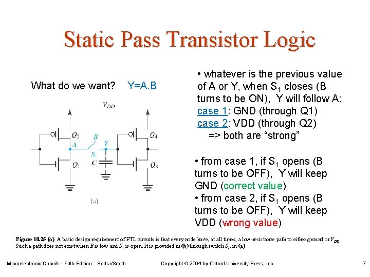
Static Pass Transistor Logic What do we want? Y=A. B • whatever is the previous value of A or Y, when S 1 closes (B turns to be ON), Y will follow A: case 1: GND (through Q 1) case 2: VDD (through Q 2) => both are “strong” • from case 1, if S 1 opens (B turns to be OFF), Y will keep GND (correct value) • from case 2, if S 1 opens (B turns to be OFF), Y will keep VDD (wrong value) Figure 10. 25 (a) A basic design requirement of PTL circuits is that every node have, at all times, a low-resistance path to either ground or VDD. Such a path does not exist when B is low and S 1 is open. It is provided in (b) through switch S 2. in (a) Microelectronic Circuits - Fifth Edition Sedra/Smith Copyright 2004 by Oxford University Press, Inc. 7

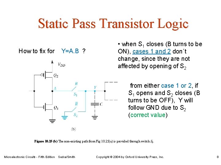
Static Pass Transistor Logic How to fix for Y=A. B ? • when S 1 closes (B turns to be ON), cases 1 and 2 don´t change, since they are not affected by opening of S 2 from either case 1 or 2, if S 1 opens and S 2 closes (B turns to be OFF), Y will follow GND due to S 2 (correct value) Figure 10. 25 (b) The non-existing path from Fig 10. 25(a) is provided through switch S 2. Microelectronic Circuits - Fifth Edition Sedra/Smith Copyright 2004 by Oxford University Press, Inc. 8

Pass Transistor Logic Problems • PTL circuits present low area consumption and low capacitance • The logic design as combination of switches is easy (as relay logic), but the high impedance factor (as in previous slide) makes it difficult • Moreover, both the static and delay characteristics are adversely affected Microelectronic Circuits - Fifth Edition Sedra/Smith Copyright 2004 by Oxford University Press, Inc. 9

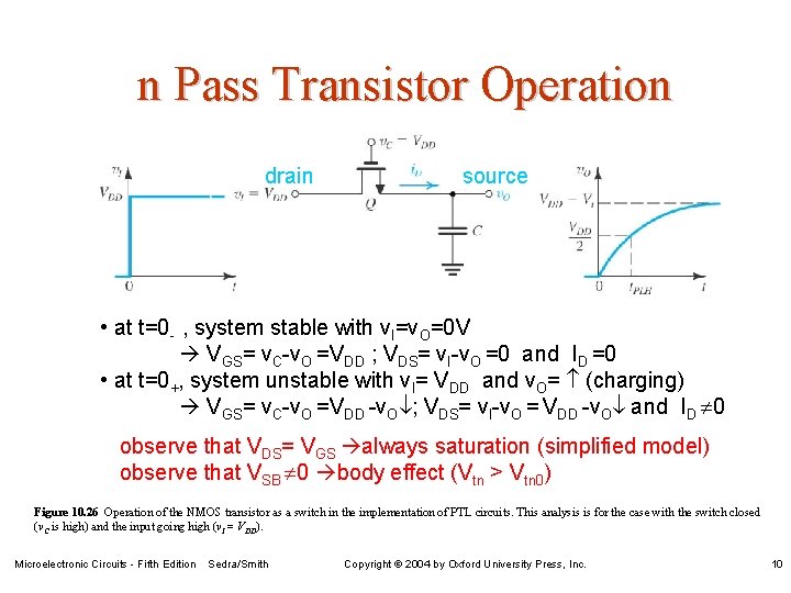
n Pass Transistor Operation drain source • at t=0 - , system stable with v. I=v. O=0 V VGS= v. C-v. O =VDD ; VDS= v. I-v. O =0 and ID =0 • at t=0+, system unstable with v. I= VDD and v. O= (charging) VGS= v. C-v. O =VDD -v. O ; VDS= v. I-v. O = VDD -v. O and ID 0 observe that VDS= VGS always saturation (simplified model) observe that VSB 0 body effect (Vtn > Vtn 0) Figure 10. 26 Operation of the NMOS transistor as a switch in the implementation of PTL circuits. This analysis is for the case with the switch closed (v. C is high) and the input going high (v. I = VDD). Microelectronic Circuits - Fifth Edition Sedra/Smith Copyright 2004 by Oxford University Press, Inc. 10

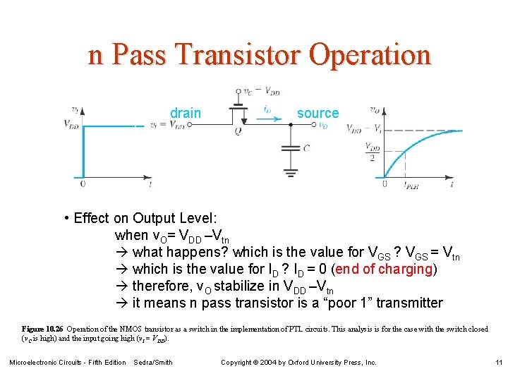
n Pass Transistor Operation drain source • Effect on Output Level: when v. O= VDD –Vtn what happens? which is the value for VGS ? VGS = Vtn which is the value for ID ? ID = 0 (end of charging) therefore, v. O stabilize in VDD –Vtn it means n pass transistor is a “poor 1” transmitter Figure 10. 26 Operation of the NMOS transistor as a switch in the implementation of PTL circuits. This analysis is for the case with the switch closed (v. C is high) and the input going high (v. I = VDD). Microelectronic Circuits - Fifth Edition Sedra/Smith Copyright 2004 by Oxford University Press, Inc. 11

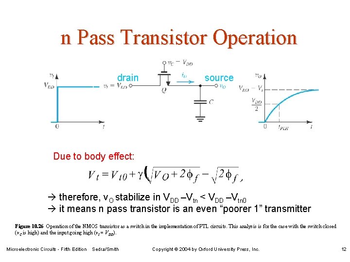
n Pass Transistor Operation drain source Due to body effect: therefore, v. O stabilize in VDD –Vtn < VDD –Vtn 0 it means n pass transistor is an even “poorer 1” transmitter Figure 10. 26 Operation of the NMOS transistor as a switch in the implementation of PTL circuits. This analysis is for the case with the switch closed (v. C is high) and the input going high (v. I = VDD). Microelectronic Circuits - Fifth Edition Sedra/Smith Copyright 2004 by Oxford University Press, Inc. 12

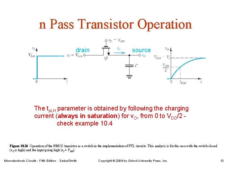
n Pass Transistor Operation drain source The tp. LH parameter is obtained by following the charging current (always in saturation) for v. O, from 0 to VDD/2 check example 10. 4 Figure 10. 26 Operation of the NMOS transistor as a switch in the implementation of PTL circuits. This analysis is for the case with the switch closed (v. C is high) and the input going high (v. I = VDD). Microelectronic Circuits - Fifth Edition Sedra/Smith Copyright 2004 by Oxford University Press, Inc. 13

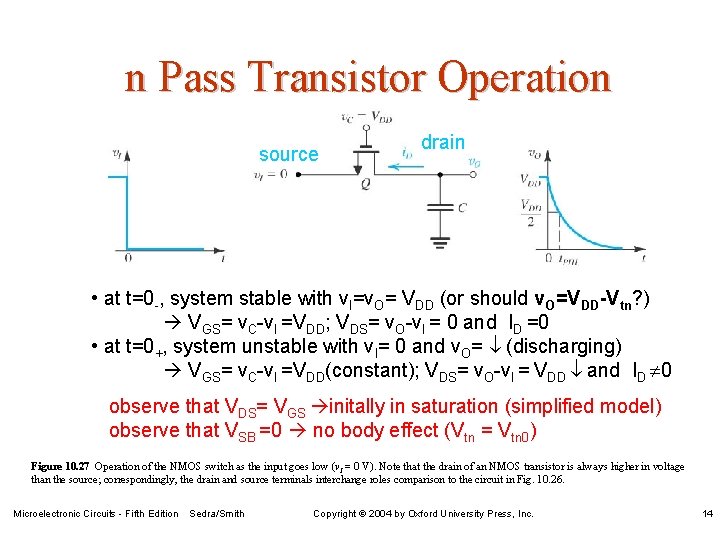
n Pass Transistor Operation source drain • at t=0 -, system stable with v. I=v. O= VDD (or should v. O=VDD-Vtn? ) VGS= v. C-v. I =VDD; VDS= v. O-v. I = 0 and ID =0 • at t=0+, system unstable with v. I= 0 and v. O= (discharging) VGS= v. C-v. I =VDD(constant); VDS= v. O-v. I = VDD and ID 0 observe that VDS= VGS initally in saturation (simplified model) observe that VSB =0 no body effect (Vtn = Vtn 0) Figure 10. 27 Operation of the NMOS switch as the input goes low (v. I = 0 V). Note that the drain of an NMOS transistor is always higher in voltage than the source; correspondingly, the drain and source terminals interchange roles comparison to the circuit in Fig. 10. 26. Microelectronic Circuits - Fifth Edition Sedra/Smith Copyright 2004 by Oxford University Press, Inc. 14

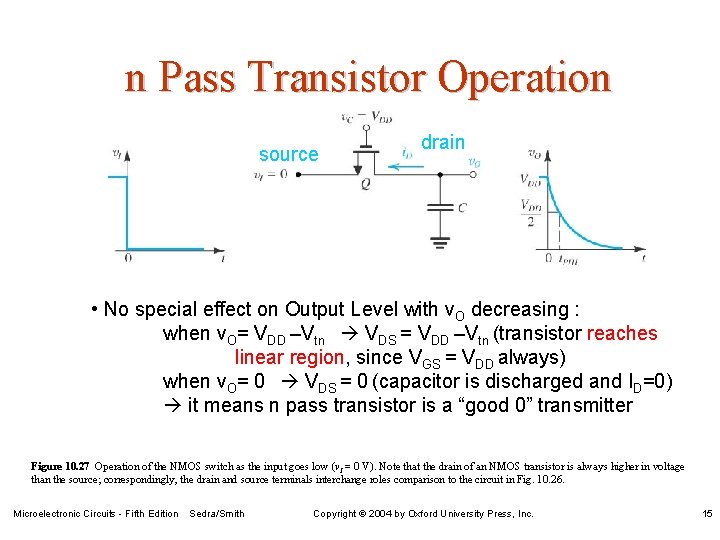
n Pass Transistor Operation source drain • No special effect on Output Level with v. O decreasing : when v. O= VDD –Vtn VDS = VDD –Vtn (transistor reaches linear region, since VGS = VDD always) when v. O= 0 VDS = 0 (capacitor is discharged and ID=0) it means n pass transistor is a “good 0” transmitter Figure 10. 27 Operation of the NMOS switch as the input goes low (v. I = 0 V). Note that the drain of an NMOS transistor is always higher in voltage than the source; correspondingly, the drain and source terminals interchange roles comparison to the circuit in Fig. 10. 26. Microelectronic Circuits - Fifth Edition Sedra/Smith Copyright 2004 by Oxford University Press, Inc. 15

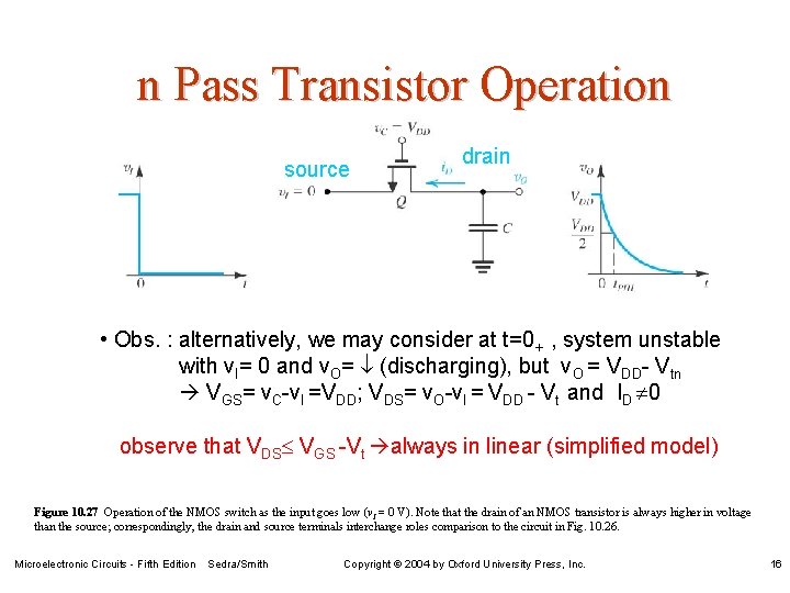
n Pass Transistor Operation source drain • Obs. : alternatively, we may consider at t=0+ , system unstable with v. I= 0 and v. O= (discharging), but v. O = VDD- Vtn VGS= v. C-v. I =VDD; VDS= v. O-v. I = VDD - Vt and ID 0 observe that VDS VGS -Vt always in linear (simplified model) Figure 10. 27 Operation of the NMOS switch as the input goes low (v. I = 0 V). Note that the drain of an NMOS transistor is always higher in voltage than the source; correspondingly, the drain and source terminals interchange roles comparison to the circuit in Fig. 10. 26. Microelectronic Circuits - Fifth Edition Sedra/Smith Copyright 2004 by Oxford University Press, Inc. 16

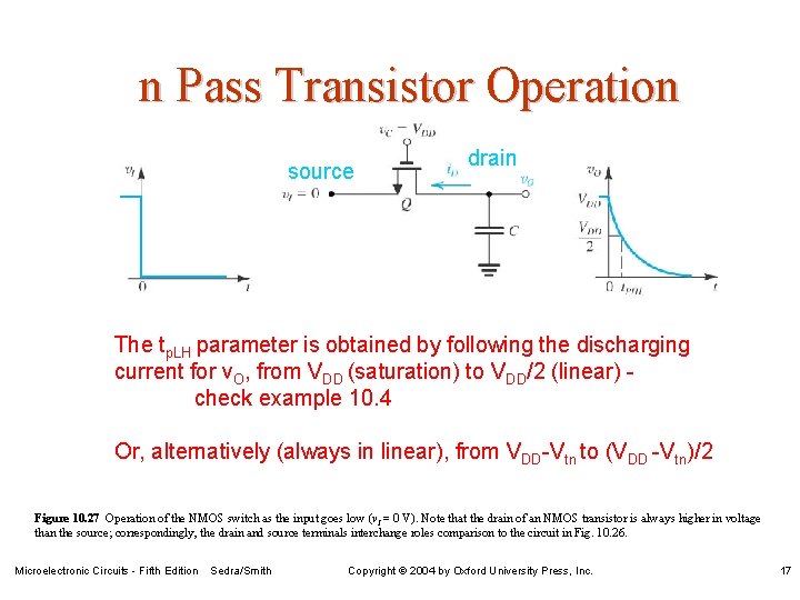
n Pass Transistor Operation source drain The tp. LH parameter is obtained by following the discharging current for v. O, from VDD (saturation) to VDD/2 (linear) check example 10. 4 Or, alternatively (always in linear), from VDD-Vtn to (VDD -Vtn)/2 Figure 10. 27 Operation of the NMOS switch as the input goes low (v. I = 0 V). Note that the drain of an NMOS transistor is always higher in voltage than the source; correspondingly, the drain and source terminals interchange roles comparison to the circuit in Fig. 10. 26. Microelectronic Circuits - Fifth Edition Sedra/Smith Copyright 2004 by Oxford University Press, Inc. 17

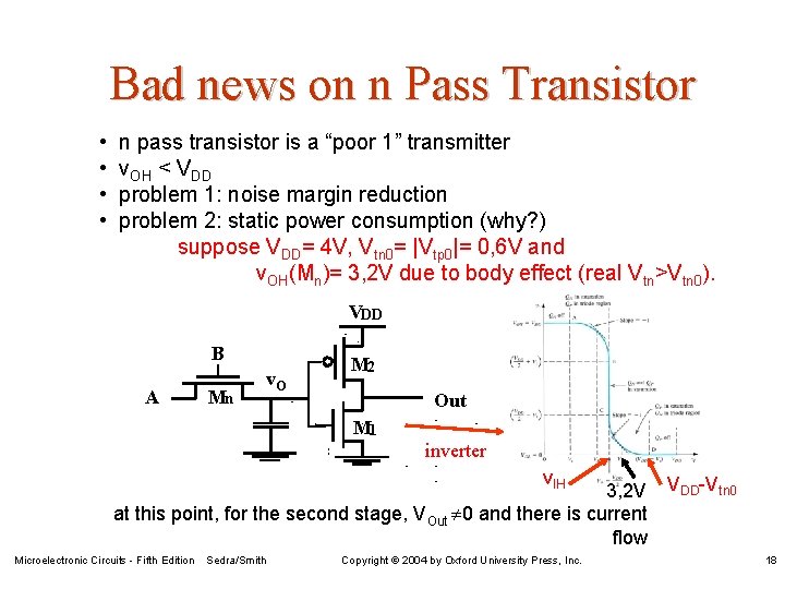
Bad news on n Pass Transistor • • n pass transistor is a “poor 1” transmitter v. OH < VDD problem 1: noise margin reduction problem 2: static power consumption (why? ) suppose VDD= 4 V, Vtn 0= |Vtp 0|= 0, 6 V and v. OH(Mn)= 3, 2 V due to body effect (real Vtn>Vtn 0). VDD B A Mn v. O M 2 Out M 1 inverter v. IH 3, 2 V at this point, for the second stage, VOut 0 and there is current flow Microelectronic Circuits - Fifth Edition Sedra/Smith Copyright 2004 by Oxford University Press, Inc. VDD-Vtn 0 18

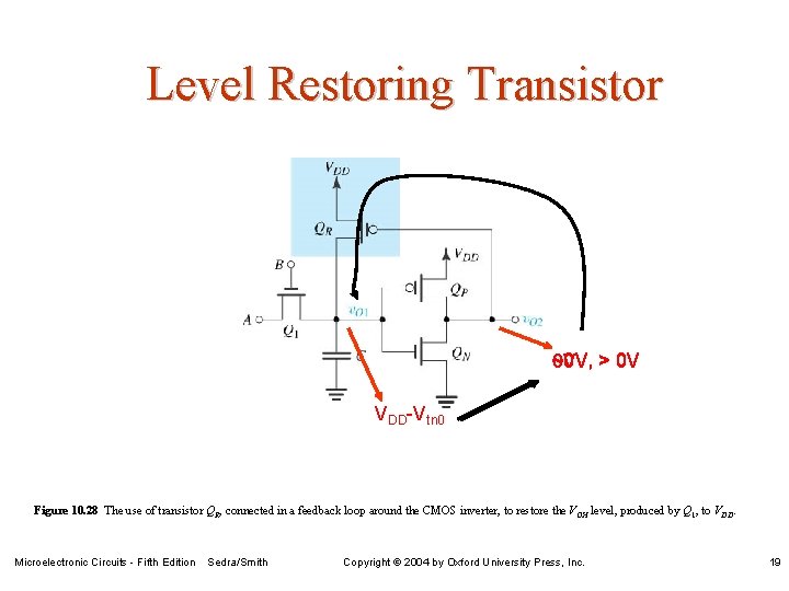
Level Restoring Transistor 0 V > 0 V ~0 V, VDD-Vtn 0 Figure 10. 28 The use of transistor QR, connected in a feedback loop around the CMOS inverter, to restore the VOH level, produced by Q 1, to VDD. Microelectronic Circuits - Fifth Edition Sedra/Smith Copyright 2004 by Oxford University Press, Inc. 19

p Pass Transistor Operation • p Pass Transistor is dual to n Pass Transistor, holding similar static and dynamic characteristics (but n transistor is faster for the same size). • p and n Pass Transistors can be used together. • P Pass Transistor is controlled by VC (= 0 for ON operation and = VDD for OFF) • p Pass Transistor is a “poor 0” transmitter, meaning it will provide at output: VDD as v. OH and |Vtp| as v. OL (Vtp < Vtp 0 due to body effect) Microelectronic Circuits - Fifth Edition Sedra/Smith Copyright 2004 by Oxford University Press, Inc. 20

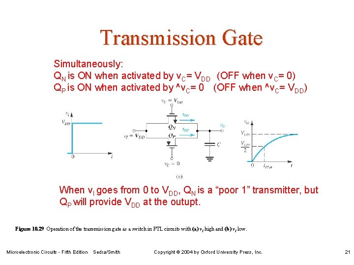
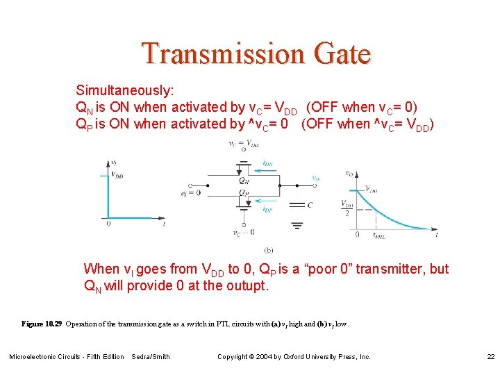
Transmission Gate Simultaneously: QN is ON when activated by v. C= VDD (OFF when v. C= 0) QP is ON when activated by ^v. C= 0 (OFF when ^v. C= VDD) When v. I goes from 0 to VDD, QN is a “poor 1” transmitter, but QP will provide VDD at the outupt. Figure 10. 29 Operation of the transmission gate as a switch in PTL circuits with (a) v. I high and (b) v. I low. Microelectronic Circuits - Fifth Edition Sedra/Smith Copyright 2004 by Oxford University Press, Inc. 21

Transmission Gate Simultaneously: QN is ON when activated by v. C= VDD (OFF when v. C= 0) QP is ON when activated by ^v. C= 0 (OFF when ^v. C= VDD) When v. I goes from VDD to 0, QP is a “poor 0” transmitter, but QN will provide 0 at the outupt. Figure 10. 29 Operation of the transmission gate as a switch in PTL circuits with (a) v. I high and (b) v. I low. Microelectronic Circuits - Fifth Edition Sedra/Smith Copyright 2004 by Oxford University Press, Inc. 22

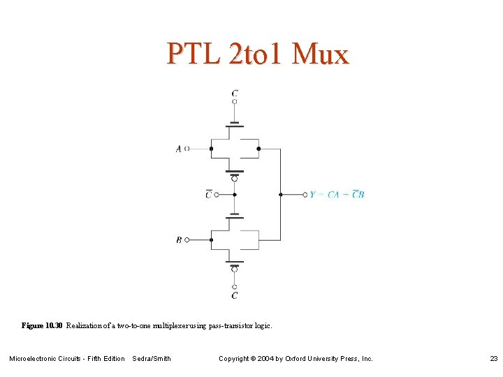
PTL 2 to 1 Mux Figure 10. 30 Realization of a two-to-one multiplexer using pass-transistor logic. Microelectronic Circuits - Fifth Edition Sedra/Smith Copyright 2004 by Oxford University Press, Inc. 23

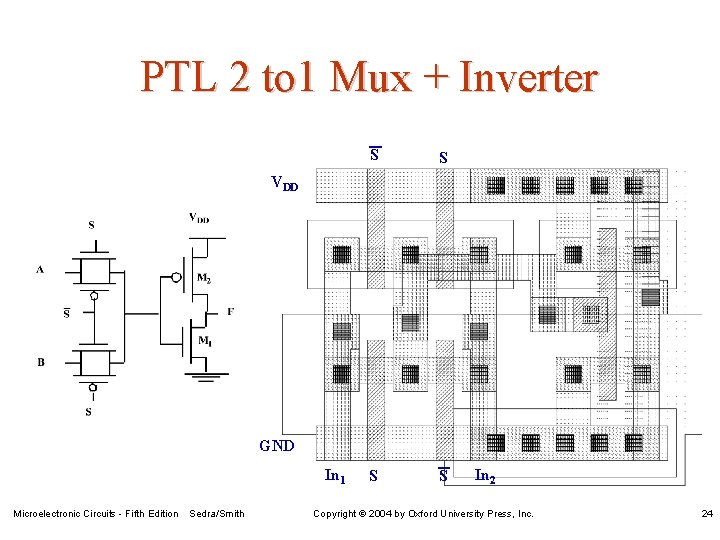
PTL 2 to 1 Mux + Inverter S S VDD GND In 1 Microelectronic Circuits - Fifth Edition Sedra/Smith In 2 Copyright 2004 by Oxford University Press, Inc. 24

PTL XOR Only 8 transistors (with inverters); the complementary logic has used 12. Figure 10. 31 Realization of the XOR function using pass-transistor logic. Microelectronic Circuits - Fifth Edition Sedra/Smith Copyright 2004 by Oxford University Press, Inc. 25

The Design Trade-offs • The use of logic families and styles are chosen according to the trade-offs on several design parameters • Voltage swing (noise margins), area, difficulty to design the circuit or to match transistors, capacitance, speed, power consumption are some of the characteristics to be analyzed. • Complementary logic CMOS, for instance, provide means to easily match n and p transistors in order to obtains balanced noise margin; PTL may provide low area consumption, but are hard to design. Microelectronic Circuits - Fifth Edition Sedra/Smith Copyright 2004 by Oxford University Press, Inc. 26

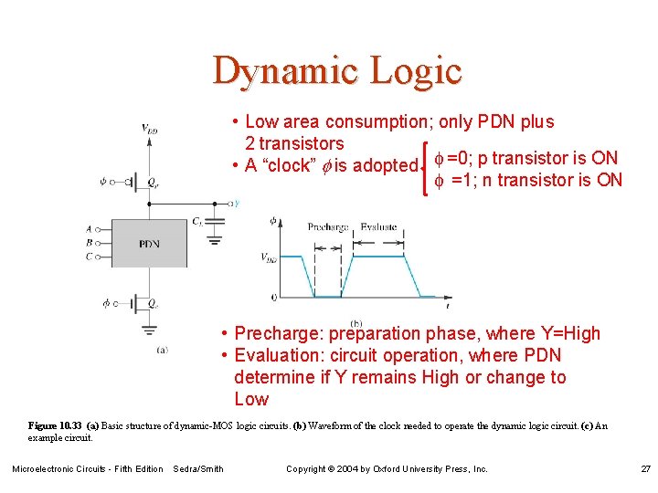
Dynamic Logic • Low area consumption; only PDN plus 2 transistors • A “clock” f is adopted f =0; p transistor is ON f =1; n transistor is ON • Precharge: preparation phase, where Y=High • Evaluation: circuit operation, where PDN determine if Y remains High or change to Low Figure 10. 33 (a) Basic structure of dynamic-MOS logic circuits. (b) Waveform of the clock needed to operate the dynamic logic circuit. (c) An example circuit. Microelectronic Circuits - Fifth Edition Sedra/Smith Copyright 2004 by Oxford University Press, Inc. 27

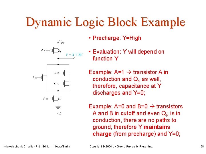
Dynamic Logic Block Example • Precharge: Y=High • Evaluation: Y will depend on function Y Example: A=1 transistor A in conduction and QN as well, therefore, capacitance at Y discharges and Y=0; Example: A=0 and B=0 transistors A and B in cutoff and even QN is in conduction, there are no paths to ground; therefore Y maintains charge (from precharge) and Y=0; Microelectronic Circuits - Fifth Edition Sedra/Smith Copyright 2004 by Oxford University Press, Inc. 28

Trade-offs At first glance • It is efficient in area. • When in evaluation, if there is no path to ground, Y is high impedance (there is no path to any other power rail), holding the charge in capacitance. • Unfortunately, there is current leakage due to reversed drain-substrate junction • Periodic refreshing of value is needed Microelectronic Circuits - Fifth Edition Sedra/Smith Copyright 2004 by Oxford University Press, Inc. 29

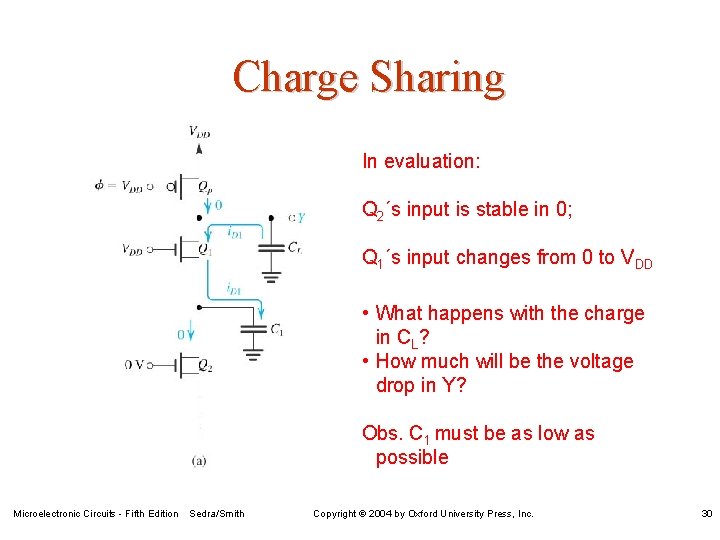
Charge Sharing In evaluation: Q 2´s input is stable in 0; Q 1´s input changes from 0 to VDD • What happens with the charge in CL? • How much will be the voltage drop in Y? Obs. C 1 must be as low as possible Microelectronic Circuits - Fifth Edition Sedra/Smith Copyright 2004 by Oxford University Press, Inc. 30

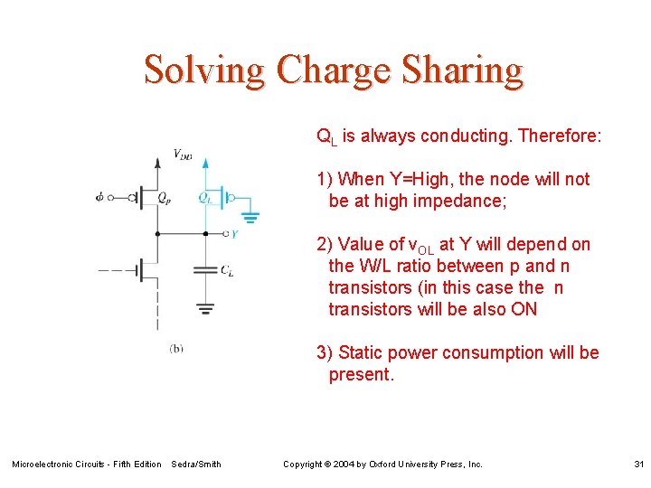
Solving Charge Sharing QL is always conducting. Therefore: 1) When Y=High, the node will not be at high impedance; 2) Value of v. OL at Y will depend on the W/L ratio between p and n transistors (in this case the n transistors will be also ON 3) Static power consumption will be present. Microelectronic Circuits - Fifth Edition Sedra/Smith Copyright 2004 by Oxford University Press, Inc. 31

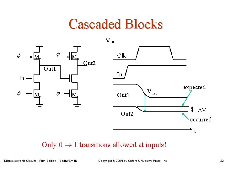
Cascaded Blocks V f Mp Out 1 Me f Out 2 In In f Clk Me Out 1 VTn Out 2 expected V occurred t Only 0 1 transitions allowed at inputs! Microelectronic Circuits - Fifth Edition Sedra/Smith Copyright 2004 by Oxford University Press, Inc. 32

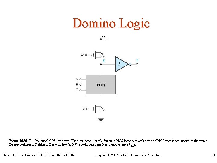
Domino Logic Figure 10. 36 The Domino CMOS logic gate. The circuit consists of a dynamic-MOS logic gate with a static-CMOS inverter connected to the output. During evaluation, Y either will remain low (at 0 V) or will make one 0 -to-1 transition (to VDD). Microelectronic Circuits - Fifth Edition Sedra/Smith Copyright 2004 by Oxford University Press, Inc. 33

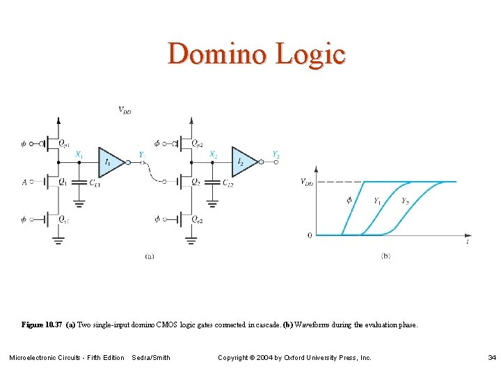
Domino Logic Figure 10. 37 (a) Two single-input domino CMOS logic gates connected in cascade. (b) Waveforms during the evaluation phase. Microelectronic Circuits - Fifth Edition Sedra/Smith Copyright 2004 by Oxford University Press, Inc. 34