Part V Memory System Design Computer Architecture Memory

- Slides: 71

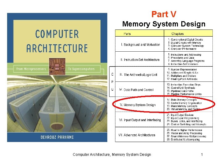
Part V Memory System Design Computer Architecture, Memory System Design 1

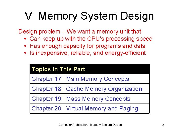
V Memory System Design problem – We want a memory unit that: • Can keep up with the CPU’s processing speed • Has enough capacity for programs and data • Is inexpensive, reliable, and energy-efficient Topics in This Part Chapter 17 Main Memory Concepts Chapter 18 Cache Memory Organization Chapter 19 Mass Memory Concepts Chapter 20 Virtual Memory and Paging Computer Architecture, Memory System Design 2

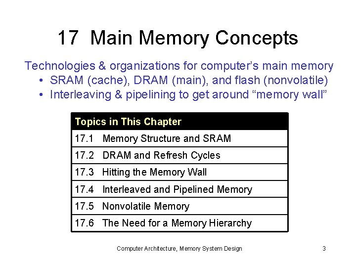
17 Main Memory Concepts Technologies & organizations for computer’s main memory • SRAM (cache), DRAM (main), and flash (nonvolatile) • Interleaving & pipelining to get around “memory wall” Topics in This Chapter 17. 1 Memory Structure and SRAM 17. 2 DRAM and Refresh Cycles 17. 3 Hitting the Memory Wall 17. 4 Interleaved and Pipelined Memory 17. 5 Nonvolatile Memory 17. 6 The Need for a Memory Hierarchy Computer Architecture, Memory System Design 3

17. 1 Memory Structure and SRAM Fig. 17. 1 Conceptual inner structure of a 2 h g SRAM chip and its shorthand representation. Computer Architecture, Memory System Design 4

Multiple-Chip SRAM Fig. 17. 2 Eight 128 K 8 SRAM chips forming a 256 K 32 memory unit. Computer Architecture, Memory System Design 5

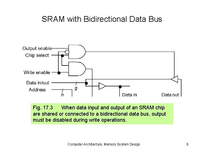
SRAM with Bidirectional Data Bus Fig. 17. 3 When data input and output of an SRAM chip are shared or connected to a bidirectional data bus, output must be disabled during write operations. Computer Architecture, Memory System Design 6

17. 2 DRAM and Refresh Cycles DRAM vs. SRAM Memory Cell Complexity Fig. 17. 4 Single-transistor DRAM cell, which is considerably simpler than SRAM cell, leads to dense, high-capacity DRAM memory chips. Computer Architecture, Memory System Design 7

DRAM Refresh Cycles and Refresh Rate Fig. 17. 5 Variations in the voltage across a DRAM cell capacitor after writing a 1 and subsequent refresh operations. Computer Architecture, Memory System Design 8

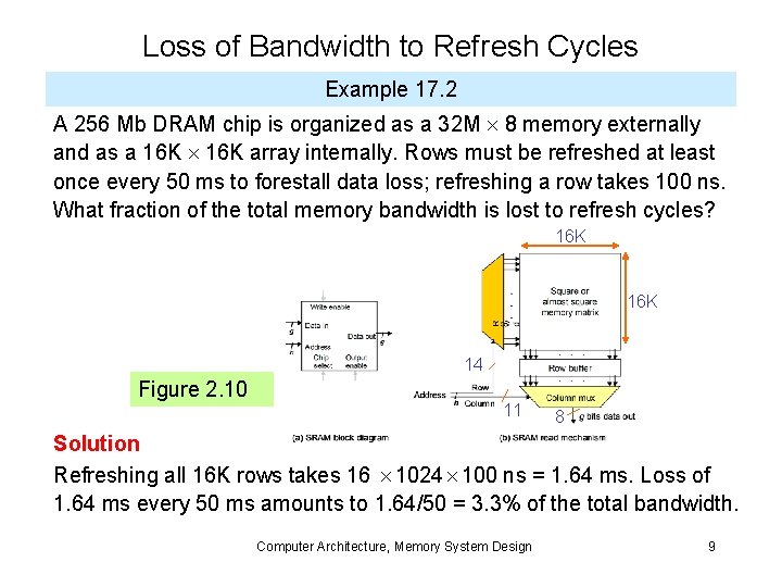
Loss of Bandwidth to Refresh Cycles Example 17. 2 A 256 Mb DRAM chip is organized as a 32 M 8 memory externally and as a 16 K array internally. Rows must be refreshed at least once every 50 ms to forestall data loss; refreshing a row takes 100 ns. What fraction of the total memory bandwidth is lost to refresh cycles? 16 K 14 Figure 2. 10 11 8 Solution Refreshing all 16 K rows takes 16 1024 100 ns = 1. 64 ms. Loss of 1. 64 ms every 50 ms amounts to 1. 64/50 = 3. 3% of the total bandwidth. Computer Architecture, Memory System Design 9

DRAM Packaging 24 -pin dual in-line package (DIP) Fig. 17. 6 Typical DRAM package housing a 16 M 4 memory. Computer Architecture, Memory System Design 10

DRAM Evolution Fig. 17. 7 Trends in DRAM main memory. Computer Architecture, Memory System Design 11

17. 3 Hitting the Memory Wall Fig. 17. 8 Memory density and capacity have grown along with the CPU power and complexity, but memory speed has not kept pace. Computer Architecture, Memory System Design 12

Bridging the CPU-Memory Speed Gap Idea: Retrieve more data from memory with each access Fig. 17. 9 Two ways of using a wide-access memory to bridge the speed gap between the processor and memory. Computer Architecture, Memory System Design 13

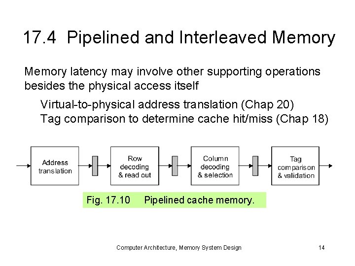
17. 4 Pipelined and Interleaved Memory latency may involve other supporting operations besides the physical access itself Virtual-to-physical address translation (Chap 20) Tag comparison to determine cache hit/miss (Chap 18) Fig. 17. 10 Pipelined cache memory. Computer Architecture, Memory System Design 14

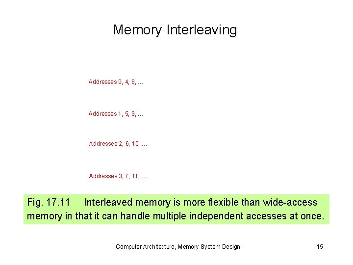
Memory Interleaving Addresses 0, 4, 8, … Addresses 1, 5, 9, … Addresses 2, 6, 10, … Addresses 3, 7, 11, … Fig. 17. 11 Interleaved memory is more flexible than wide-access memory in that it can handle multiple independent accesses at once. Computer Architecture, Memory System Design 15

17. 5 Nonvolatile Memory ROM PROM EPROM Fig. 17. 12 Read-only memory organization, with the fixed contents shown on the right. Computer Architecture, Memory System Design 16

Flash Memory Fig. 17. 13 EEPROM or Flash memory organization. Each memory cell is built of a floating-gate MOS transistor. Computer Architecture, Memory System Design 17

17. 6 The Need for a Memory Hierarchy The widening speed gap between CPU and main memory Processor operations take of the order of 1 ns Memory access requires 10 s or even 100 s of ns Memory bandwidth limits the instruction execution rate Each instruction executed involves at least one memory access Hence, a few to 100 s of MIPS is the best that can be achieved A fast buffer memory can help bridge the CPU-memory gap The fastest memories are expensive and thus not very large A second (third? ) intermediate cache level is thus often used Computer Architecture, Memory System Design 18

Typical Levels in a Hierarchical Memory Fig. 17. 14 Names and key characteristics of levels in a memory hierarchy. Computer Architecture, Memory System Design 19

18 Cache Memory Organization Processor speed is improving at a faster rate than memory’s • Processor-memory speed gap has been widening • Cache is to main as desk drawer is to file cabinet Topics in This Chapter 18. 1 The Need for a Cache 18. 2 What Makes a Cache Work? 18. 3 Direct-Mapped Cache 18. 4 Set-Associative Cache 18. 5 Cache and Main Memory 18. 6 Improving Cache Performance Computer Architecture, Memory System Design 20

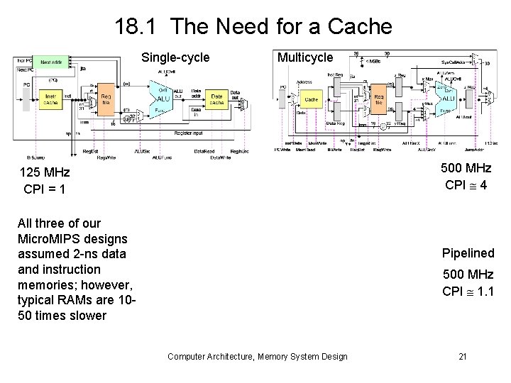
18. 1 The Need for a Cache Single-cycle Multicycle 500 MHz CPI 4 125 MHz CPI = 1 All three of our Micro. MIPS designs assumed 2 -ns data and instruction memories; however, typical RAMs are 1050 times slower Pipelined 500 MHz CPI 1. 1 Computer Architecture, Memory System Design 21

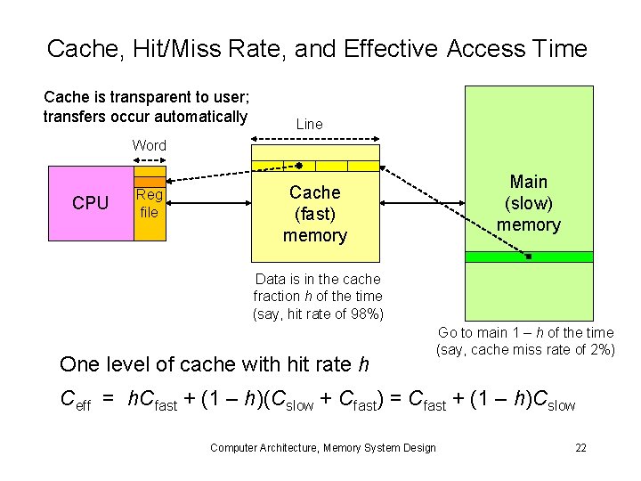
Cache, Hit/Miss Rate, and Effective Access Time Cache is transparent to user; transfers occur automatically Line Word CPU Reg file Main (slow) memory Cache (fast) memory Data is in the cache fraction h of the time (say, hit rate of 98%) One level of cache with hit rate h Go to main 1 – h of the time (say, cache miss rate of 2%) Ceff = h. Cfast + (1 – h)(Cslow + Cfast) = Cfast + (1 – h)Cslow Computer Architecture, Memory System Design 22

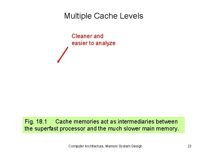
Multiple Cache Levels Cleaner and easier to analyze Fig. 18. 1 Cache memories act as intermediaries between the superfast processor and the much slower main memory. Computer Architecture, Memory System Design 23

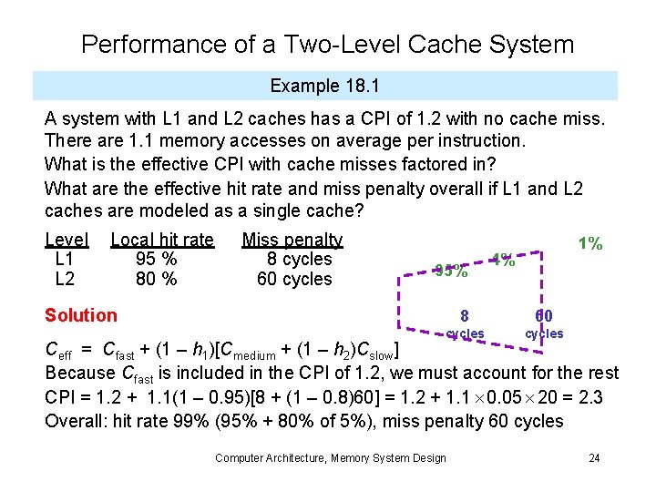
Performance of a Two-Level Cache System Example 18. 1 A system with L 1 and L 2 caches has a CPI of 1. 2 with no cache miss. There are 1. 1 memory accesses on average per instruction. What is the effective CPI with cache misses factored in? What are the effective hit rate and miss penalty overall if L 1 and L 2 caches are modeled as a single cache? Level L 1 L 2 Local hit rate 95 % 80 % Miss penalty 8 cycles 60 cycles 95% Solution 1% 4% 8 60 cycles Ceff = Cfast + (1 – h 1)[Cmedium + (1 – h 2)Cslow] Because Cfast is included in the CPI of 1. 2, we must account for the rest CPI = 1. 2 + 1. 1(1 – 0. 95)[8 + (1 – 0. 8)60] = 1. 2 + 1. 1 0. 05 20 = 2. 3 Overall: hit rate 99% (95% + 80% of 5%), miss penalty 60 cycles Computer Architecture, Memory System Design 24

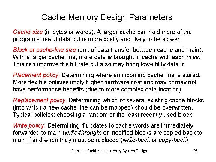
Cache Memory Design Parameters Cache size (in bytes or words). A larger cache can hold more of the program’s useful data but is more costly and likely to be slower. Block or cache-line size (unit of data transfer between cache and main). With a larger cache line, more data is brought in cache with each miss. This can improve the hit rate but also may bring low-utility data in. Placement policy. Determining where an incoming cache line is stored. More flexible policies imply higher hardware cost and may or may not have performance benefits (due to more complex data location). Replacement policy. Determining which of several existing cache blocks (into which a new cache line can be mapped) should be overwritten. Typical policies: choosing a random or the least recently used block. Write policy. Determining if updates to cache words are immediately forwarded to main (write-through) or modified blocks are copied back to main if and when they must be replaced (write-back or copy-back). Computer Architecture, Memory System Design 25

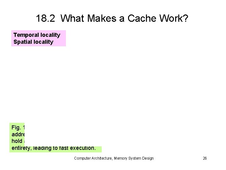
18. 2 What Makes a Cache Work? Temporal locality Spatial locality Fig. 18. 2 Assuming no conflict in address mapping, the cache will hold a small program loop in its entirety, leading to fast execution. Computer Architecture, Memory System Design 26

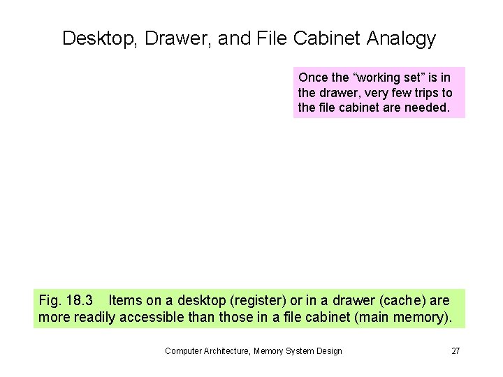
Desktop, Drawer, and File Cabinet Analogy Once the “working set” is in the drawer, very few trips to the file cabinet are needed. Fig. 18. 3 Items on a desktop (register) or in a drawer (cache) are more readily accessible than those in a file cabinet (main memory). Computer Architecture, Memory System Design 27

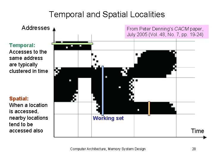
Temporal and Spatial Localities Addresses From Peter Denning’s CACM paper, July 2005 (Vol. 48, No. 7, pp. 19 -24) Temporal: Accesses to the same address are typically clustered in time Spatial: When a location is accessed, nearby locations tend to be accessed also Working set Time Computer Architecture, Memory System Design 28

Caching Benefits Related to Amdahl’s Law Example 18. 2 In the drawer & file cabinet analogy, assume a hit rate h in the drawer. Formulate the situation shown in Fig. 18. 2 in terms of Amdahl’s law. Solution Without the drawer, a document is accessed in 30 s. So, fetching 1000 documents, say, would take 30 000 s. The drawer causes a fraction h of the cases to be done 6 times as fast, with access time unchanged for the remaining 1 – h. Speedup is thus 1/(1 – h + h/6) = 6 / (6 – 5 h). Improving the drawer access time can increase the speedup factor but as long as the miss rate remains at 1 – h, the speedup can never exceed 1 / (1 – h). Given h = 0. 9, for instance, the speedup is 4, with the upper bound being 10 for an extremely short drawer access time. Note: Some would place everything on their desktop, thinking that this yields even greater speedup. This strategy is not recommended! Computer Architecture, Memory System Design 29

Compulsory, Capacity, and Conflict Misses Compulsory misses: With on-demand fetching, first access to any item is a miss. Some “compulsory” misses can be avoided by prefetching. Capacity misses: We have to oust some items to make room for others. This leads to misses that are not incurred with an infinitely large cache. Conflict misses: Occasionally, there is free room, or space occupied by useless data, but the mapping/placement scheme forces us to displace useful items to bring in other items. This may lead to misses in future. Given a fixed-size cache, dictated, e. g. , by cost factors or availability of space on the processor chip, compulsory and capacity misses are pretty much fixed. Conflict misses, on the other hand, are influenced by the data mapping scheme which is under our control. We study two popular mapping schemes: direct and set-associative. Computer Architecture, Memory System Design 30

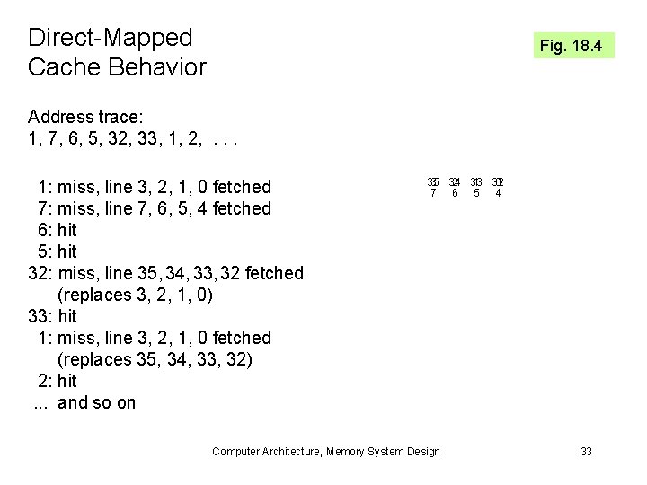
18. 3 Direct-Mapped Cache Fig. 18. 4 Direct-mapped cache holding 32 words within eight 4 -word lines. Each line is associated with a tag and a valid bit. Computer Architecture, Memory System Design 31

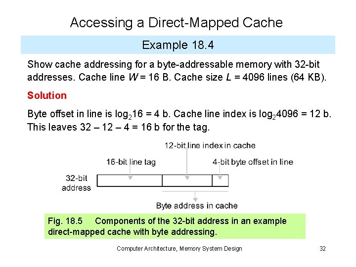
Accessing a Direct-Mapped Cache Example 18. 4 Show cache addressing for a byte-addressable memory with 32 -bit addresses. Cache line W = 16 B. Cache size L = 4096 lines (64 KB). Solution Byte offset in line is log 216 = 4 b. Cache line index is log 24096 = 12 b. This leaves 32 – 12 – 4 = 16 b for the tag. Fig. 18. 5 Components of the 32 -bit address in an example direct-mapped cache with byte addressing. Computer Architecture, Memory System Design 32

Direct-Mapped Cache Behavior Fig. 18. 4 Address trace: 1, 7, 6, 5, 32, 33, 1, 2, . . . 1: miss, line 3, 2, 1, 0 fetched 7: miss, line 7, 6, 5, 4 fetched 6: hit 5: hit 32: miss, line 35, 34, 33, 32 fetched (replaces 3, 2, 1, 0) 33: hit 1: miss, line 3, 2, 1, 0 fetched (replaces 35, 34, 33, 32) 2: hit. . . and so on 35 3 34 2 33 1 32 0 7 6 5 4 Computer Architecture, Memory System Design 33

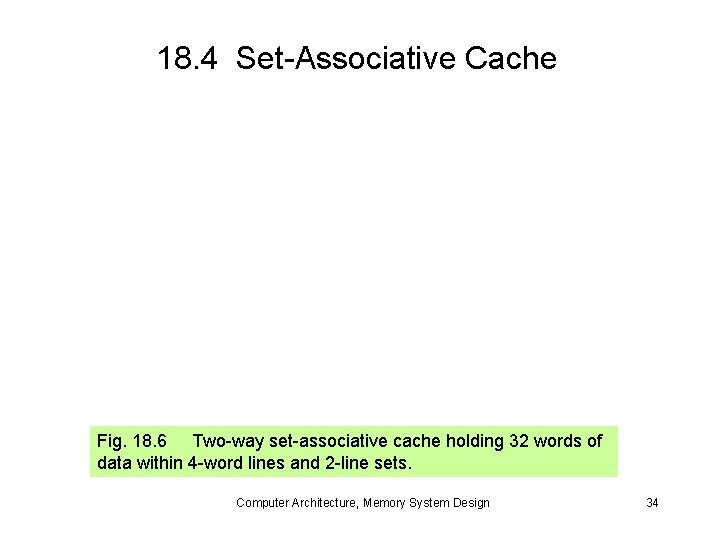
18. 4 Set-Associative Cache Fig. 18. 6 Two-way set-associative cache holding 32 words of data within 4 -word lines and 2 -line sets. Computer Architecture, Memory System Design 34

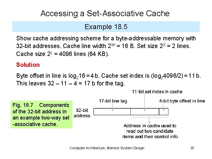
Accessing a Set-Associative Cache Example 18. 5 Show cache addressing scheme for a byte-addressable memory with 32 -bit addresses. Cache line width 2 W = 16 B. Set size 2 S = 2 lines. Cache size 2 L = 4096 lines (64 KB). Solution Byte offset in line is log 216 = 4 b. Cache set index is (log 24096/2) = 11 b. This leaves 32 – 11 – 4 = 17 b for the tag. Fig. 18. 7 Components of the 32 -bit address in an example two-way set -associative cache. Computer Architecture, Memory System Design 35

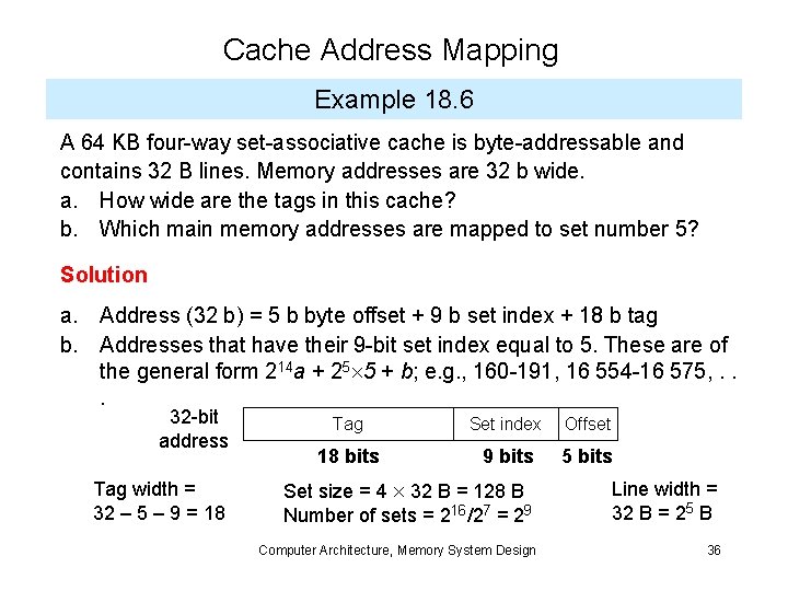
Cache Address Mapping Example 18. 6 A 64 KB four-way set-associative cache is byte-addressable and contains 32 B lines. Memory addresses are 32 b wide. a. How wide are the tags in this cache? b. Which main memory addresses are mapped to set number 5? Solution a. Address (32 b) = 5 b byte offset + 9 b set index + 18 b tag b. Addresses that have their 9 -bit set index equal to 5. These are of the general form 214 a + 25 5 + b; e. g. , 160 -191, 16 554 -16 575, . . . 32 -bit address Tag width = 32 – 5 – 9 = 18 Tag Set index Offset 18 bits 9 bits 5 bits Set size = 4 32 B = 128 B Number of sets = 216/27 = 29 Line width = 32 B = 25 B Computer Architecture, Memory System Design 36

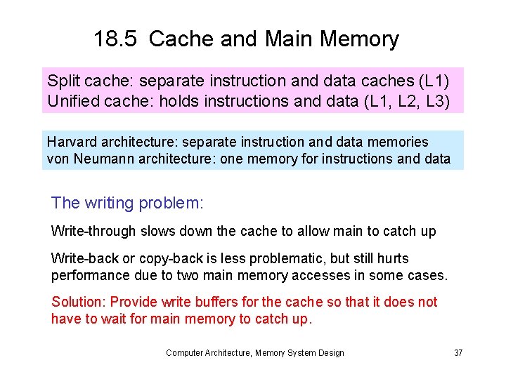
18. 5 Cache and Main Memory Split cache: separate instruction and data caches (L 1) Unified cache: holds instructions and data (L 1, L 2, L 3) Harvard architecture: separate instruction and data memories von Neumann architecture: one memory for instructions and data The writing problem: Write-through slows down the cache to allow main to catch up Write-back or copy-back is less problematic, but still hurts performance due to two main memory accesses in some cases. Solution: Provide write buffers for the cache so that it does not have to wait for main memory to catch up. Computer Architecture, Memory System Design 37

Faster Main-Cache Data Transfers Fig. 18. 8 A 256 Mb DRAM chip organized as a 32 M 8 memory module: four such chips could form a 128 MB main memory unit. Computer Architecture, Memory System Design 38

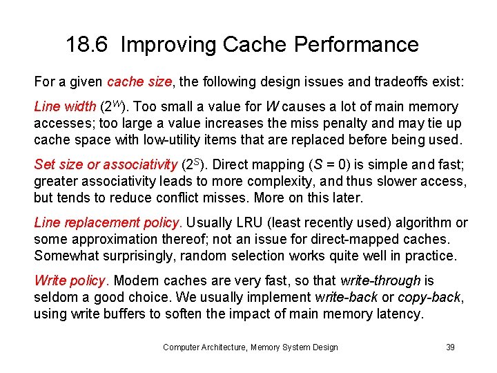
18. 6 Improving Cache Performance For a given cache size, the following design issues and tradeoffs exist: Line width (2 W). Too small a value for W causes a lot of main memory accesses; too large a value increases the miss penalty and may tie up cache space with low-utility items that are replaced before being used. Set size or associativity (2 S). Direct mapping (S = 0) is simple and fast; greater associativity leads to more complexity, and thus slower access, but tends to reduce conflict misses. More on this later. Line replacement policy. Usually LRU (least recently used) algorithm or some approximation thereof; not an issue for direct-mapped caches. Somewhat surprisingly, random selection works quite well in practice. Write policy. Modern caches are very fast, so that write-through is seldom a good choice. We usually implement write-back or copy-back, using write buffers to soften the impact of main memory latency. Computer Architecture, Memory System Design 39

Effect of Associativity on Cache Performance Fig. 18. 9 Performance improvement of caches with increased associativity. Computer Architecture, Memory System Design 40

19 Mass Memory Concepts Today’s main memory is huge, but still inadequate for all needs • Magnetic disks provide extended and back-up storage • Optical disks & disk arrays are other mass storage options Topics in This Chapter 19. 1 Disk Memory Basics 19. 2 Organizing Data on Disk 19. 3 Disk Performance 19. 4 Disk Caching 19. 5 Disk Arrays and RAID 19. 6 Other Types of Mass Memory Computer Architecture, Memory System Design 41

19. 1 Disk Memory Basics Fig. 19. 1 Disk memory elements and key terms. Computer Architecture, Memory System Design 42

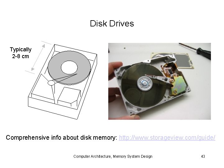
Disk Drives Typically 2 -82 cm - 8 cm Comprehensive info about disk memory: http: //www. storageview. com/guide/ Computer Architecture, Memory System Design 43

Access Time for a Disk The three components of disk access time. Disks that spin faster have a shorter average and worst-case access time. Computer Architecture, Memory System Design 44

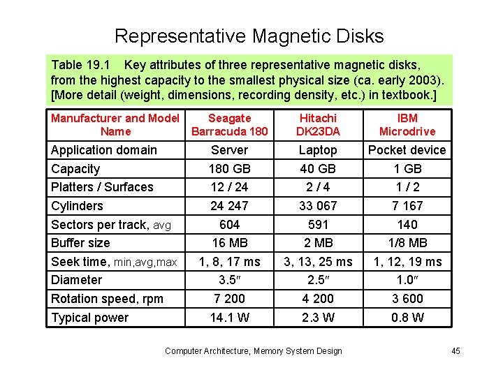
Representative Magnetic Disks Table 19. 1 Key attributes of three representative magnetic disks, from the highest capacity to the smallest physical size (ca. early 2003). [More detail (weight, dimensions, recording density, etc. ) in textbook. ] Manufacturer and Model Seagate Name Barracuda 180 Application domain Capacity Platters / Surfaces Cylinders Sectors per track, avg Buffer size Seek time, min, avg, max Diameter Rotation speed, rpm Typical power Server 180 GB 12 / 24 24 247 604 16 MB 1, 8, 17 ms 3. 5 7 200 14. 1 W Hitachi DK 23 DA IBM Microdrive Laptop 40 GB 2/4 33 067 591 2 MB 3, 13, 25 ms 2. 5 4 200 2. 3 W Pocket device 1 GB 1/2 7 167 140 1/8 MB 1, 12, 19 ms 1. 0 3 600 0. 8 W Computer Architecture, Memory System Design 45

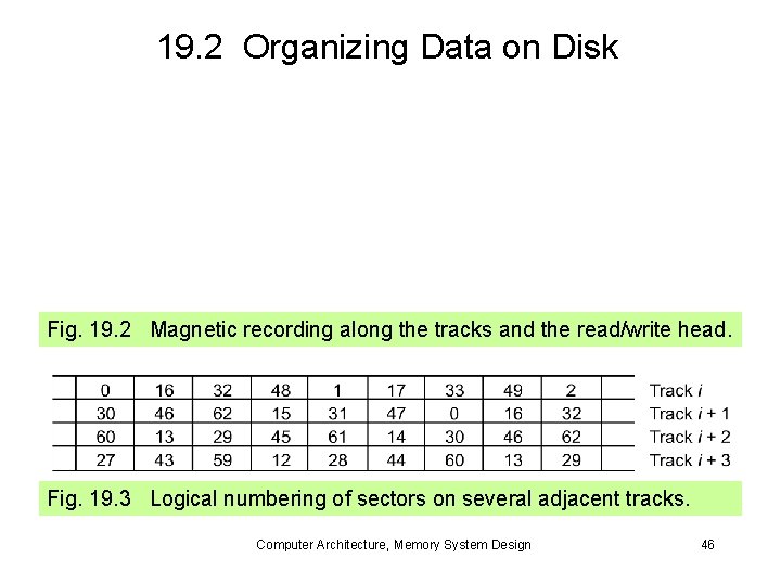
19. 2 Organizing Data on Disk Fig. 19. 2 Magnetic recording along the tracks and the read/write head. Fig. 19. 3 Logical numbering of sectors on several adjacent tracks. Computer Architecture, Memory System Design 46

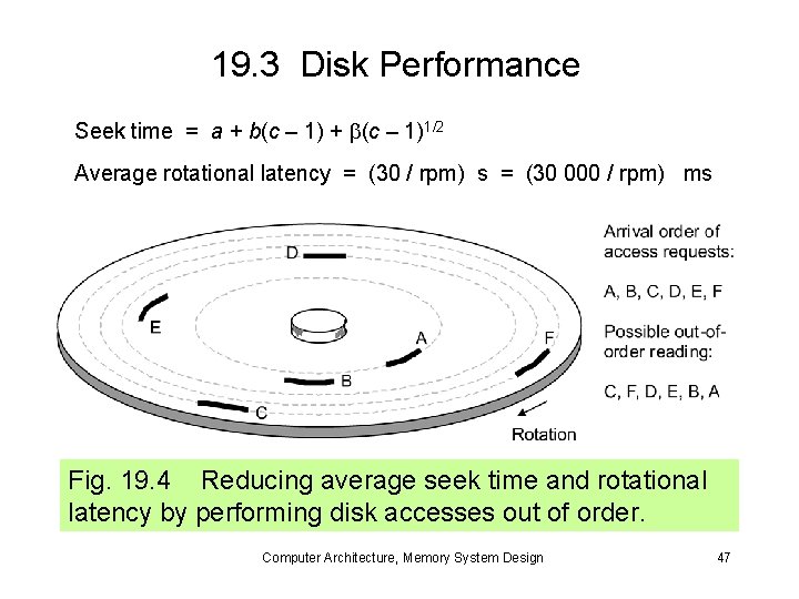
19. 3 Disk Performance Seek time = a + b(c – 1)1/2 Average rotational latency = (30 / rpm) s = (30 000 / rpm) ms Fig. 19. 4 Reducing average seek time and rotational latency by performing disk accesses out of order. Computer Architecture, Memory System Design 47

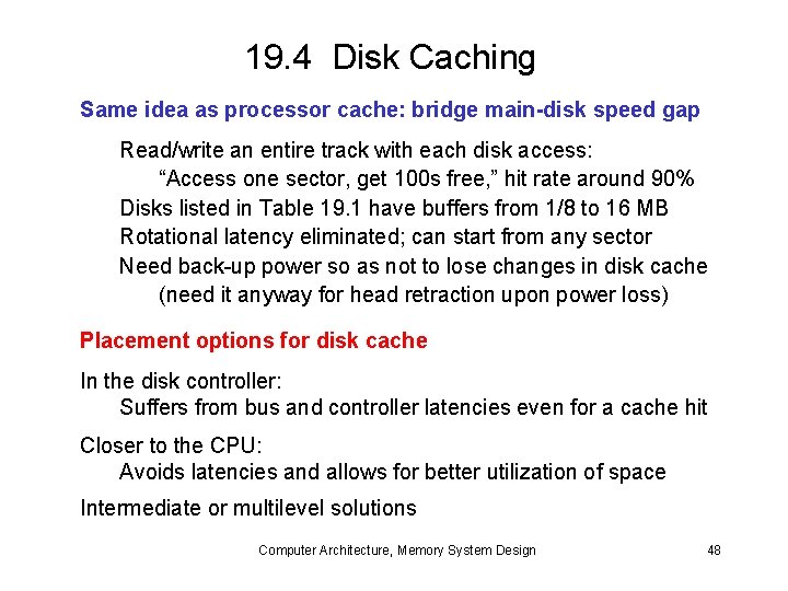
19. 4 Disk Caching Same idea as processor cache: bridge main-disk speed gap Read/write an entire track with each disk access: “Access one sector, get 100 s free, ” hit rate around 90% Disks listed in Table 19. 1 have buffers from 1/8 to 16 MB Rotational latency eliminated; can start from any sector Need back-up power so as not to lose changes in disk cache (need it anyway for head retraction upon power loss) Placement options for disk cache In the disk controller: Suffers from bus and controller latencies even for a cache hit Closer to the CPU: Avoids latencies and allows for better utilization of space Intermediate or multilevel solutions Computer Architecture, Memory System Design 48

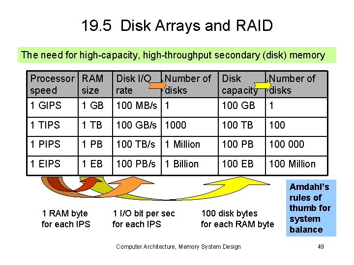
19. 5 Disk Arrays and RAID The need for high-capacity, high-throughput secondary (disk) memory Processor RAM speed size Disk I/O rate 1 GIPS 1 GB 1 TIPS Disk capacity Number of disks 100 MB/s 1 100 GB 1 1 TB 100 GB/s 1000 100 TB 100 1 PIPS 1 PB 100 TB/s 1 Million 100 PB 100 000 1 EIPS 1 EB 100 PB/s 1 Billion 100 EB 100 Million 1 RAM byte for each IPS Number of disks 1 I/O bit per sec for each IPS 100 disk bytes for each RAM byte Computer Architecture, Memory System Design Amdahl’s rules of thumb for system balance 49

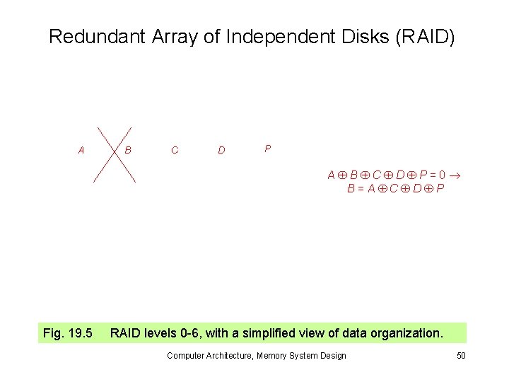
Redundant Array of Independent Disks (RAID) A B C D P=0 B=A C D P Fig. 19. 5 RAID levels 0 -6, with a simplified view of data organization. Computer Architecture, Memory System Design 50

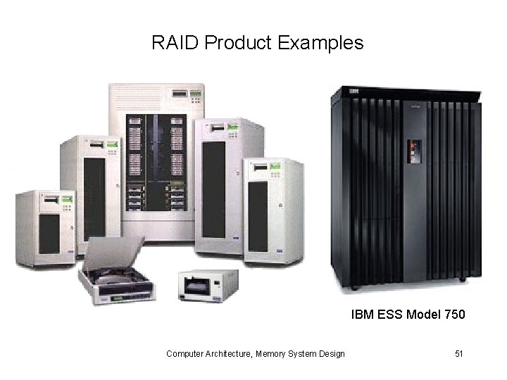
RAID Product Examples IBM ESS Model 750 Computer Architecture, Memory System Design 51

19. 6 Other Types of Mass Memory Fig. 3. 12 Magnetic and optical disk memory units. Computer Architecture, Memory System Design 52

Optical Disks Spiral, rather than concentric, tracks Fig. 19. 6 Simplified view of recording format and access mechanism for data on a CD-ROM or DVD-ROM. Computer Architecture, Memory System Design 53

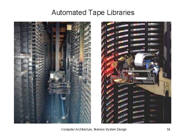
Automated Tape Libraries Computer Architecture, Memory System Design 54

20 Virtual Memory and Paging Managing data transfers between main & mass is cumbersome • Virtual memory automates this process • Key to virtual memory’s success is the same as for cache Topics in This Chapter 20. 1 The Need for Virtual Memory 20. 2 Address Translation in Virtual Memory 20. 3 Translation Lookaside Buffer 20. 4 Page Placement and Replacement 20. 5 Main and Mass Memories 20. 6 Improving Virtual Memory Performance Computer Architecture, Memory System Design 55

20. 1 The Need for Virtual Memory Fig. 20. 1 Program segments in main memory and on disk. Computer Architecture, Memory System Design 56

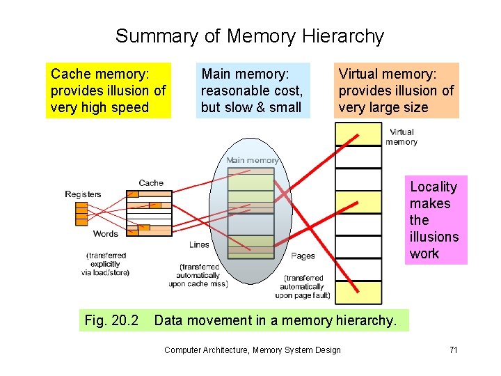
Memory Hierarchy: The Big Picture Fig. 20. 2 Data movement in a memory hierarchy. Computer Architecture, Memory System Design 57

20. 2 Address Translation in Virtual Memory Fig. 20. 3 Example 20. 1 Virtual-to-physical address translation parameters. Determine the parameters in Fig. 20. 3 for 32 -bit virtual addresses, 4 KB pages, and 128 MB byte-addressable main memory. Solution: Physical addresses are 27 b, byte offset in page is 12 b; thus, virtual (physical) page numbers are 32 – 12 = 20 b (15 b) Computer Architecture, Memory System Design 58

Page Tables and Address Translation Fig. 20. 4 The role of page table in the virtual-to-physical address translation process. Computer Architecture, Memory System Design 59

Protection and Sharing in Virtual Memory Fig. 20. 5 Virtual memory as a facilitator of sharing and memory protection. Computer Architecture, Memory System Design 60

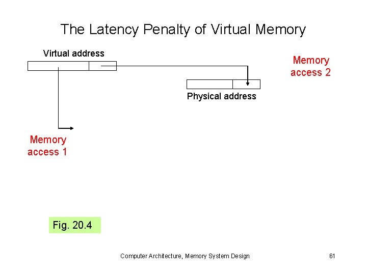
The Latency Penalty of Virtual Memory Virtual address Memory access 2 Physical address Memory access 1 Fig. 20. 4 Computer Architecture, Memory System Design 61

20. 3 Translation Lookaside Buffer Fig. 20. 6 Virtual-to-physical address translation by a TLB and how the resulting physical address is used to access the cache memory. Computer Architecture, Memory System Design 62

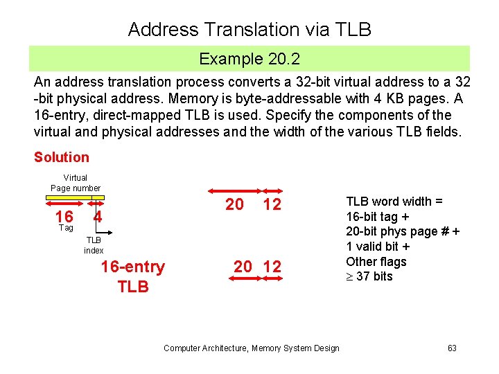
Address Translation via TLB Example 20. 2 An address translation process converts a 32 -bit virtual address to a 32 -bit physical address. Memory is byte-addressable with 4 KB pages. A 16 -entry, direct-mapped TLB is used. Specify the components of the virtual and physical addresses and the width of the various TLB fields. Solution Virtual Page number 16 Tag 20 4 12 TLB index 16 -entry TLB 20 12 Computer Architecture, Memory System Design TLB word width = 16 -bit tag + 20 -bit phys page # + 1 valid bit + Other flags 37 bits 63

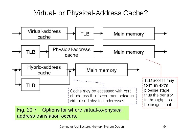
Virtual- or Physical-Address Cache? Cache may be accessed with part of address that is common between virtual and physical addresses TLB access may form an extra pipeline stage, thus the penalty in throughput can be insignificant Fig. 20. 7 Options for where virtual-to-physical address translation occurs. Computer Architecture, Memory System Design 64

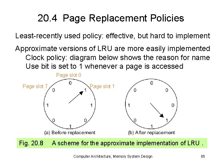
20. 4 Page Replacement Policies Least-recently used policy: effective, but hard to implement Approximate versions of LRU are more easily implemented Clock policy: diagram below shows the reason for name Use bit is set to 1 whenever a page is accessed Page slot 0 Page slot 7 Fig. 20. 8 Page slot 1 A scheme for the approximate implementation of LRU. Computer Architecture, Memory System Design 65

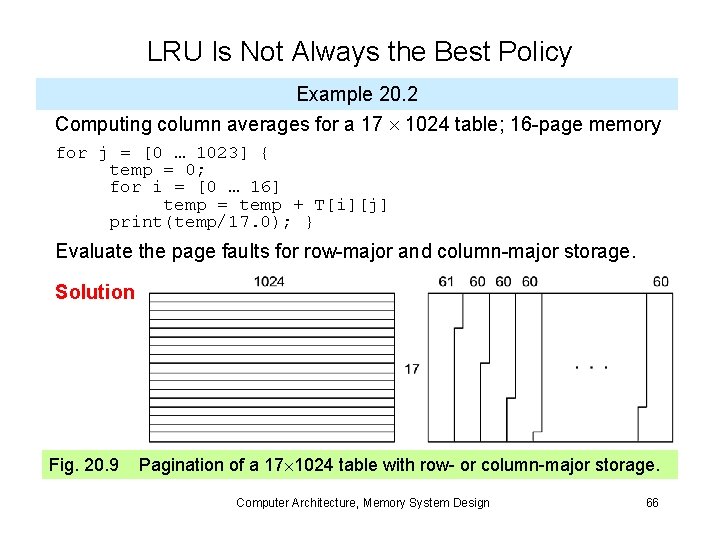
LRU Is Not Always the Best Policy Example 20. 2 Computing column averages for a 17 1024 table; 16 -page memory for j = [0 … 1023] { temp = 0; for i = [0 … 16] temp = temp + T[i][j] print(temp/17. 0); } Evaluate the page faults for row-major and column-major storage. Solution Fig. 20. 9 Pagination of a 17 1024 table with row- or column-major storage. Computer Architecture, Memory System Design 66

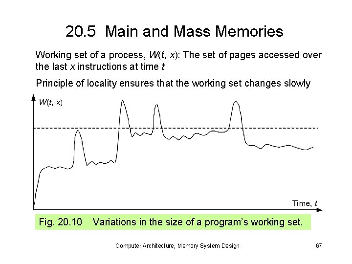
20. 5 Main and Mass Memories Working set of a process, W(t, x): The set of pages accessed over the last x instructions at time t Principle of locality ensures that the working set changes slowly Fig. 20. 10 Variations in the size of a program’s working set. Computer Architecture, Memory System Design 67

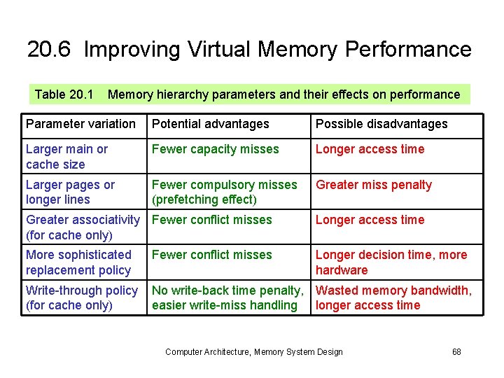
20. 6 Improving Virtual Memory Performance Table 20. 1 Memory hierarchy parameters and their effects on performance Parameter variation Potential advantages Possible disadvantages Larger main or cache size Fewer capacity misses Longer access time Larger pages or longer lines Fewer compulsory misses (prefetching effect) Greater miss penalty Greater associativity Fewer conflict misses (for cache only) Longer access time More sophisticated replacement policy Fewer conflict misses Longer decision time, more hardware Write-through policy (for cache only) No write-back time penalty, Wasted memory bandwidth, easier write-miss handling longer access time Computer Architecture, Memory System Design 68

Impact of Technology on Virtual Memory Fig. 20. 11 Trends in disk, main memory, and CPU speeds. Computer Architecture, Memory System Design 69

Performance Impact of the Replacement Policy Fig. 20. 12 Dependence of page faults on the number of pages allocated and the page replacement policy Computer Architecture, Memory System Design 70

Summary of Memory Hierarchy Cache memory: provides illusion of very high speed Main memory: reasonable cost, but slow & small Virtual memory: provides illusion of very large size Locality makes the illusions work Fig. 20. 2 Data movement in a memory hierarchy. Computer Architecture, Memory System Design 71