Part IV Data Path and Control Computer Architecture

- Slides: 31

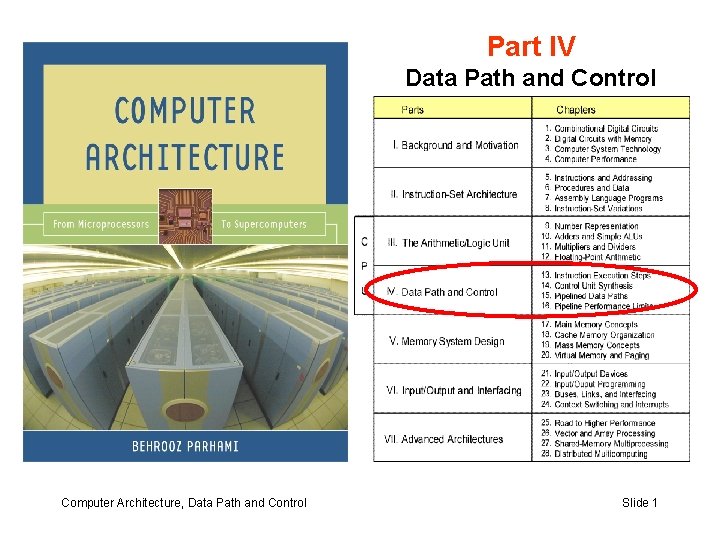
Part IV Data Path and Control Computer Architecture, Data Path and Control Slide 1

IV Data Path and Control Topics in This Part Chapter 13 Instruction Execution Steps Chapter 14 Control Unit Synthesis Computer Architecture, Data Path and Control Slide 2

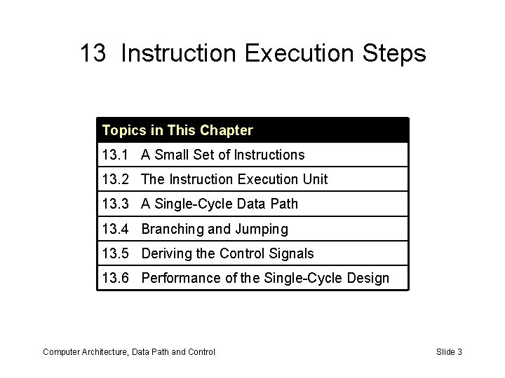
13 Instruction Execution Steps Topics in This Chapter 13. 1 A Small Set of Instructions 13. 2 The Instruction Execution Unit 13. 3 A Single-Cycle Data Path 13. 4 Branching and Jumping 13. 5 Deriving the Control Signals 13. 6 Performance of the Single-Cycle Design Computer Architecture, Data Path and Control Slide 3

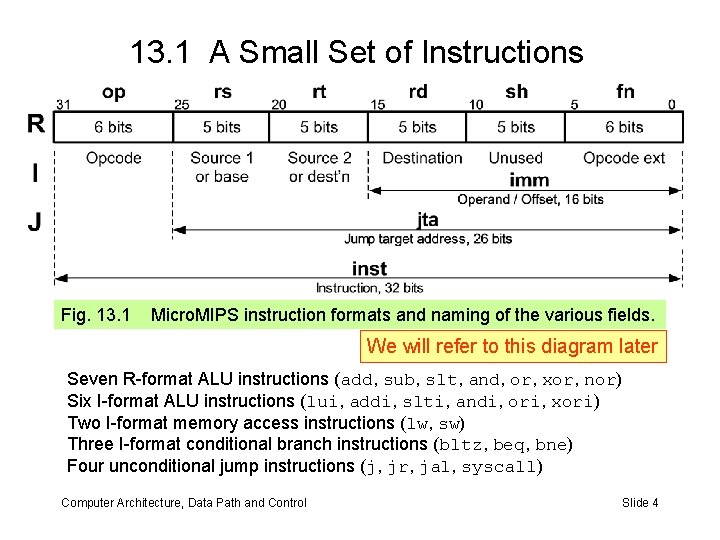
13. 1 A Small Set of Instructions Fig. 13. 1 Micro. MIPS instruction formats and naming of the various fields. We will refer to this diagram later Seven R-format ALU instructions (add, sub, slt, and, or, xor, nor) Six I-format ALU instructions (lui, addi, slti, andi, ori, xori) Two I-format memory access instructions (lw, sw) Three I-format conditional branch instructions (bltz, beq, bne) Four unconditional jump instructions (j, jr, jal, syscall) Computer Architecture, Data Path and Control Slide 4

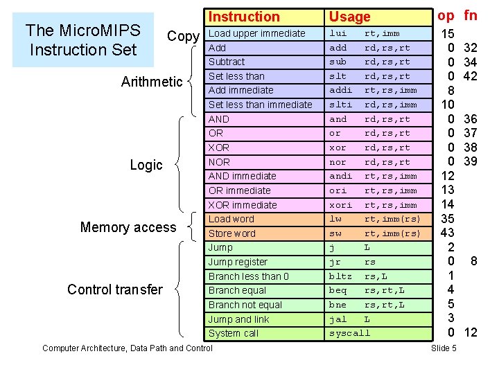
The Micro. MIPS Instruction Set Copy Arithmetic Logic Memory access Control transfer Instruction Usage Load upper immediate Add Subtract Set less than Add immediate Set less than immediate AND OR XOR NOR AND immediate OR immediate XOR immediate Load word Store word Jump register Branch less than 0 Branch equal Branch not equal Jump and link System call lui rt, imm add rd, rs, rt sub rd, rs, rt slt rd, rs, rt addi rt, rs, imm slti rd, rs, imm and rd, rs, rt or rd, rs, rt xor rd, rs, rt nor rd, rs, rt andi rt, rs, imm ori rt, rs, imm xori rt, rs, imm lw rt, imm(rs) sw rt, imm(rs) j L jr rs bltz rs, L beq rs, rt, L bne rs, rt, L jal L syscall Computer Architecture, Data Path and Control op fn 15 0 0 0 8 10 0 0 12 13 14 35 43 2 0 1 4 5 3 0 Slide 5 32 34 42 36 37 38 39 8 12

13. 2 The Instruction Execution Unit Fig. 13. 2 Abstract view of the instruction execution unit for Micro. MIPS. For naming of instruction fields, see Fig. 13. 1. Computer Architecture, Data Path and Control Slide 6

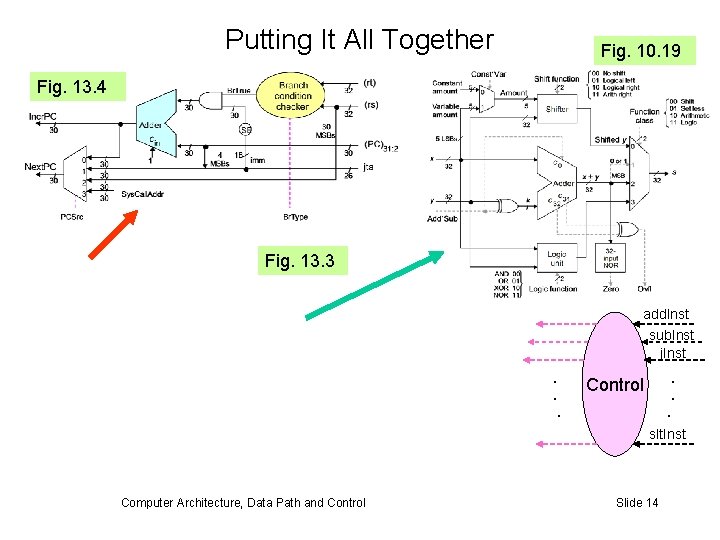
13. 3 A Single-Cycle Data Path Fig. 13. 3 Key elements of the single-cycle Micro. MIPS data path. Computer Architecture, Data Path and Control Slide 7

lui An ALU for Micro. MIPS imm Fig. 10. 19 A multifunction ALU with 8 control signals (2 for function class, 1 arithmetic, 3 shift, 2 logic) specifying the operation. Computer Architecture, Data Path and Control Slide 8

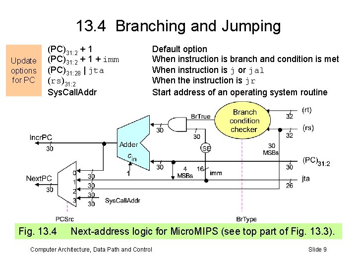
13. 4 Branching and Jumping Update options for PC (PC)31: 2 + 1 + imm (PC)31: 28 | jta (rs)31: 2 Sys. Call. Addr Default option When instruction is branch and condition is met When instruction is j or jal When the instruction is jr Start address of an operating system routine Fig. 13. 4 Next-address logic for Micro. MIPS (see top part of Fig. 13. 3). Computer Architecture, Data Path and Control Slide 9

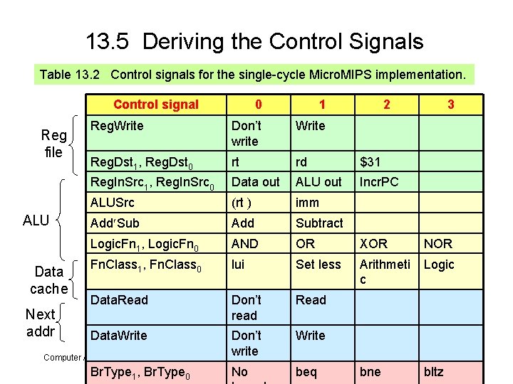
13. 5 Deriving the Control Signals Table 13. 2 Control signals for the single-cycle Micro. MIPS implementation. Control signal Reg file ALU Data cache Next addr 0 1 Reg. Write Don’t write Write Reg. Dst 1, Reg. Dst 0 rt rd $31 Reg. In. Src 1, Reg. In. Src 0 Data out ALU out Incr. PC ALUSrc (rt ) imm Add Subtract Logic. Fn 1, Logic. Fn 0 AND OR XOR NOR Fn. Class 1, Fn. Class 0 lui Set less Arithmeti c Logic Data. Read Don’t read Read Data. Write Don’t write Write No beq Computer Architecture, Data Path and Control Br. Type 1, Br. Type 0 2 3 Slide 10 bne bltz

Control Signal Settings Table 13. 3 Computer Architecture, Data Path and Control Slide 11

Instruction Decoding Fig. 13. 5 Instruction decoder for Micro. MIPS built of two 6 -to-64 decoders. Computer Architecture, Data Path and Control Slide 12

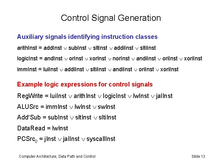
Control Signal Generation Auxiliary signals identifying instruction classes arith. Inst = add. Inst sub. Inst slt. Inst addi. Inst slti. Inst logic. Inst = and. Inst or. Inst xor. Inst nor. Inst andi. Inst ori. Inst xori. Inst imm. Inst = lui. Inst addi. Inst slti. Inst andi. Inst ori. Inst xori. Inst Example logic expressions for control signals Reg. Write = lui. Inst arith. Inst logic. Inst lw. Inst jal. Inst ALUSrc = imm. Inst lw. Inst sw. Inst Add Sub = sub. Inst slti. Inst Data. Read = lw. Inst PCSrc 0 = j. Inst jal. Inst syscall. Inst Computer Architecture, Data Path and Control Slide 13

Putting It All Together Fig. 10. 19 Fig. 13. 4 Fig. 13. 3 add. Inst sub. Inst j. Inst. . Control. . slt. Inst Computer Architecture, Data Path and Control Slide 14

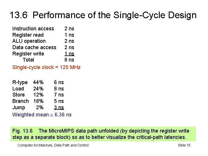
13. 6 Performance of the Single-Cycle Design Instruction access 2 ns Register read 1 ns ALU operation 2 ns Data cache access 2 ns Register write 1 ns Total 8 ns Single-cycle clock = 125 MHz R-type 44% 6 ns Load 24% 8 ns Store 12% 7 ns Branch 18% 5 ns Jump 2% 3 ns Weighted mean 6. 36 ns Fig. 13. 6 The Micro. MIPS data path unfolded (by depicting the register write step as a separate block) so as to better visualize the critical-path latencies. Computer Architecture, Data Path and Control Slide 15

14 Control Unit Synthesis Topics in This Chapter 14. 1 A Multicycle Implementation 14. 2 Choosing the Clock Cycle 14. 3 The Control State Machine 14. 4 Performance of the Multicycle Design 14. 5 Microprogramming 14. 6 Exception Handling Computer Architecture, Data Path and Control Slide 16

14. 1 A Multicycle Implementation Fig. 14. 1 Single-cycle versus multicycle instruction execution. Computer Architecture, Data Path and Control Slide 17

A Multicycle Data Path Fig. 14. 2 Abstract view of a multicycle instruction execution unit for Micro. MIPS. For naming of instruction fields, see Fig. 13. 1. Computer Architecture, Data Path and Control Slide 18

Multicycle Data Path with Control Signals Shown Fig. 14. 3 Key elements of the multicycle Micro. MIPS data path. Computer Architecture, Data Path and Control Slide 19

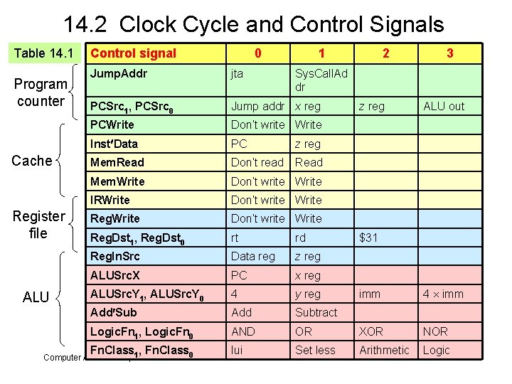
14. 2 Clock Cycle and Control Signals Table 14. 1 Program counter Cache Register file ALU Control signal 0 1 2 3 Jump. Addr jta PCSrc 1, PCSrc 0 Jump addr x reg z reg ALU out PCWrite Don’t write Write Inst Data PC z reg Mem. Read Don’t read Read Mem. Write Don’t write Write IRWrite Don’t write Write Reg. Dst 1, Reg. Dst 0 rt rd $31 Reg. In. Src Data reg z reg ALUSrc. X PC x reg ALUSrc. Y 1, ALUSrc. Y 0 4 y reg imm 4 imm Add Subtract Logic. Fn 1, Logic. Fn 0 AND OR XOR NOR Fn. Class , Fn. Class lui Set less Arithmetic Logic 1 0 Computer Architecture, Data Path and Control Sys. Call. Ad dr Slide 20

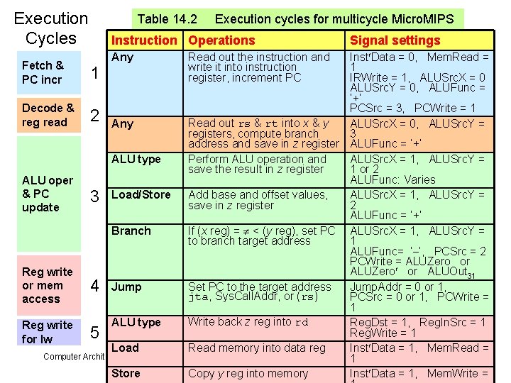
Execution Cycles Table 14. 2 Execution cycles for multicycle Micro. MIPS Instruction Operations Inst Data = 0, Mem. Read = 1 1 IRWrite = 1, ALUSrc. X = 0 ALUSrc. Y = 0, ALUFunc = ‘+’ PCSrc = 3, PCWrite = 1 Decode & 2 reg read Read out rs & rt into x & y Any ALUSrc. X = 0, ALUSrc. Y = 3 registers, compute branch address and save in z register ALUFunc = ‘+’ ALU type Perform ALU operation and ALUSrc. X = 1, ALUSrc. Y = save the result in z register 1 or 2 ALUFunc: Varies ALU oper & PC ALUSrc. X = 1, ALUSrc. Y = 3 Load/Store Add base and offset values, save in z register 2 update ALUFunc = ‘+’ Branch If (x reg) = < (y reg), set PC ALUSrc. X = 1, ALUSrc. Y = to branch target address 1 ALUFunc= ‘ ’, PCSrc = 2 PCWrite = ALUZero or ALUOut 31 Reg write or mem Set PC to the target address Jump. Addr = 0 or 1, 4 Jump jta, Sys. Call. Addr, or (rs) PCSrc = 0 or 1, PCWrite = access 1 Write back z reg into rd ALU type Reg. Dst = 1, Reg. In. Src = 1 Reg write Reg. Write = 1 5 for lw Load Read memory into data reg Inst Data = 1, Mem. Read = Computer Architecture, Data Path and Control Slide 21 1 Store Copy y reg into memory Inst Data = 1, Mem. Write = Fetch & PC incr Any Read out the instruction and write it into instruction register, increment PC Signal settings

14. 3 The Control State Machine Fig. 14. 4 The control state machine for multicycle Micro. MIPS. Computer Architecture, Data Path and Control Slide 22

State and Instruction Decoding addi. Inst Fig. 14. 5 State and instruction decoders for multicycle Micro. MIPS. Computer Architecture, Data Path and Control Slide 23

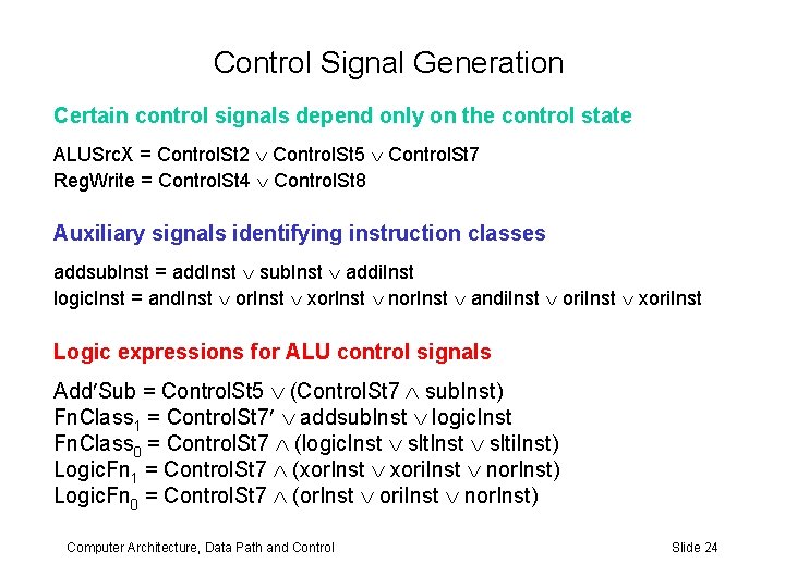
Control Signal Generation Certain control signals depend only on the control state ALUSrc. X = Control. St 2 Control. St 5 Control. St 7 Reg. Write = Control. St 4 Control. St 8 Auxiliary signals identifying instruction classes addsub. Inst = add. Inst sub. Inst addi. Inst logic. Inst = and. Inst or. Inst xor. Inst nor. Inst andi. Inst ori. Inst xori. Inst Logic expressions for ALU control signals Add Sub = Control. St 5 (Control. St 7 sub. Inst) Fn. Class 1 = Control. St 7 addsub. Inst logic. Inst Fn. Class 0 = Control. St 7 (logic. Inst slti. Inst) Logic. Fn 1 = Control. St 7 (xor. Inst xori. Inst nor. Inst) Logic. Fn 0 = Control. St 7 (or. Inst ori. Inst nor. Inst) Computer Architecture, Data Path and Control Slide 24

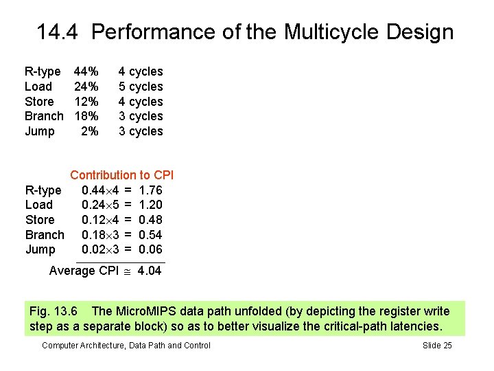
14. 4 Performance of the Multicycle Design R-type Load Store Branch Jump 44% 4 cycles 24% 5 cycles 12% 4 cycles 18% 3 cycles 2% 3 cycles Contribution to CPI R-type 0. 44 4 = 1. 76 Load 0. 24 5 = 1. 20 Store 0. 12 4 = 0. 48 Branch 0. 18 3 = 0. 54 Jump 0. 02 3 = 0. 06 _______________ Average CPI 4. 04 Fig. 13. 6 The Micro. MIPS data path unfolded (by depicting the register write step as a separate block) so as to better visualize the critical-path latencies. Computer Architecture, Data Path and Control Slide 25

14. 5 Microprogramming Fig. 14. 6 Possible 22 -bit microinstruction format for Micro. MIPS. Computer Architecture, Data Path and Control Slide 26

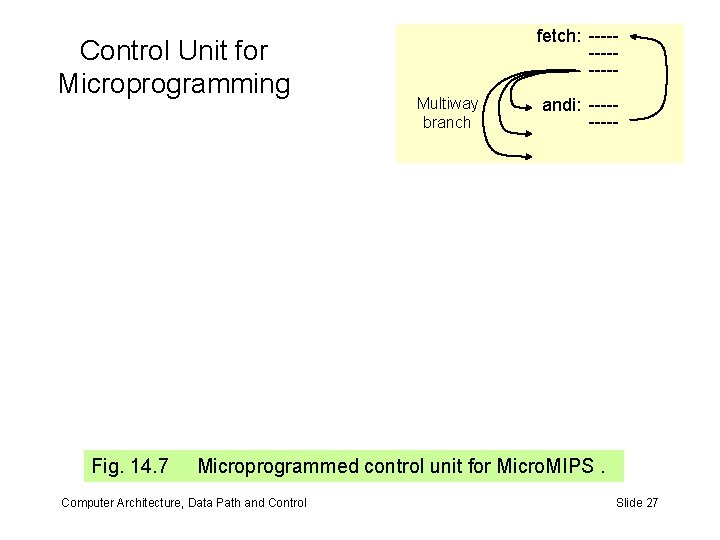
Control Unit for Microprogramming fetch: ------Multiway branch andi: ---- Fig. 14. 7 Microprogrammed control unit for Micro. MIPS. Computer Architecture, Data Path and Control Slide 27

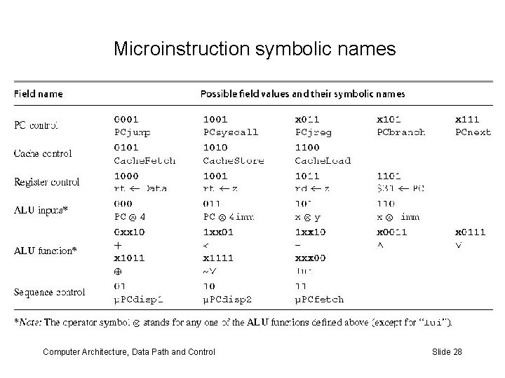
Microinstruction symbolic names Computer Architecture, Data Path and Control Slide 28

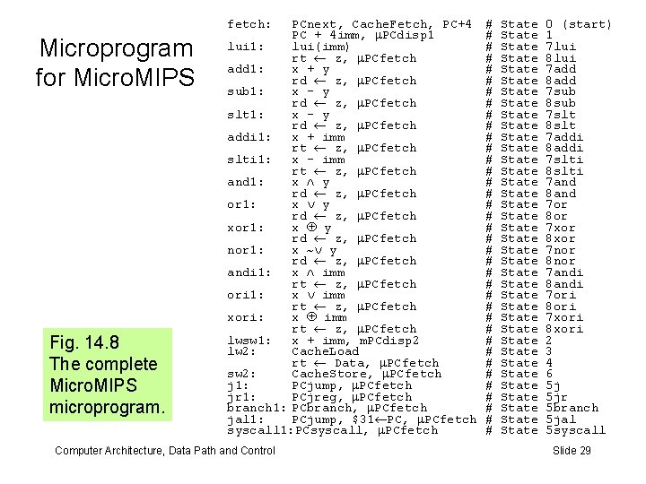
fetch: Microprogram for Micro. MIPS Fig. 14. 8 The complete Micro. MIPS microprogram. PCnext, Cache. Fetch, PC+4 PC + 4 imm, m. PCdisp 1 lui 1: lui(imm) rt ¬ z, m. PCfetch add 1: x + y rd ¬ z, m. PCfetch sub 1: x - y rd ¬ z, m. PCfetch slt 1: x - y rd ¬ z, m. PCfetch addi 1: x + imm rt ¬ z, m. PCfetch slti 1: x - imm rt ¬ z, m. PCfetch and 1: x y rd ¬ z, m. PCfetch or 1: x y rd ¬ z, m. PCfetch xor 1: x Å y rd ¬ z, m. PCfetch nor 1: x ~ y rd ¬ z, m. PCfetch andi 1: x imm rt ¬ z, m. PCfetch ori 1: x imm rt ¬ z, m. PCfetch xori: x Å imm rt ¬ z, m. PCfetch lwsw 1: x + imm, m. PCdisp 2 lw 2: Cache. Load rt ¬ Data, m. PCfetch sw 2: Cache. Store, m. PCfetch j 1: PCjump, m. PCfetch jr 1: PCjreg, m. PCfetch branch 1: PCbranch, m. PCfetch jal 1: PCjump, $31¬PC, m. PCfetch syscall 1: PCsyscall, m. PCfetch Computer Architecture, Data Path and Control # # # # # # # # # # State State State State State State State State State State 0 (start) 1 7 lui 8 lui 7 add 8 add 7 sub 8 sub 7 slt 8 slt 7 addi 8 addi 7 slti 8 slti 7 and 8 and 7 or 8 or 7 xor 8 xor 7 nor 8 nor 7 andi 8 andi 7 ori 8 ori 7 xori 8 xori 2 3 4 6 5 j 5 jr 5 branch 5 jal 5 syscall Slide 29

14. 6 Exception Handling Exceptions and interrupts alter the normal program flow Examples of exceptions (things that can go wrong): ALU operation leads to overflow (incorrect result is obtained) Opcode field holds a pattern not representing a legal operation Cache error-code checker deems an accessed word invalid Sensor signals a hazardous condition (e. g. , overheating) Exception handler is an OS program that takes care of the problem Derives correct result of overflowing computation, if possible Invalid operation may be a software-implemented instruction Interrupts are similar, but usually have external causes (e. g. , I/O) Computer Architecture, Data Path and Control Slide 30

Exception Control States Fig. 14. 10 Exception states 9 and 10 added to the control state machine. Computer Architecture, Data Path and Control Slide 31