Part 01 Proposal and Overview Dual Modulus Prescaler

- Slides: 51

Part 01: Proposal and Overview

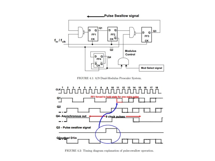
Dual Modulus Prescaler Using Current Mode Logic Goals • 2. 5 GHz Operation • 8/9 Dual Modulus • 0. 18 u. M BSIM 3 Model


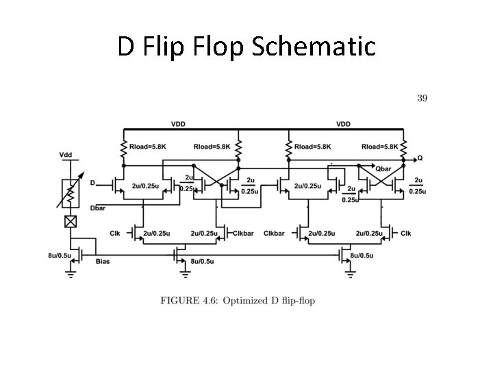
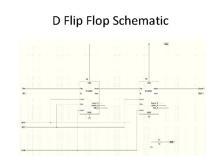
D Flip Flop Schematic

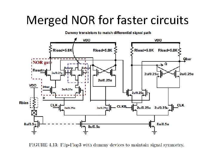
Merged NOR for faster circuits

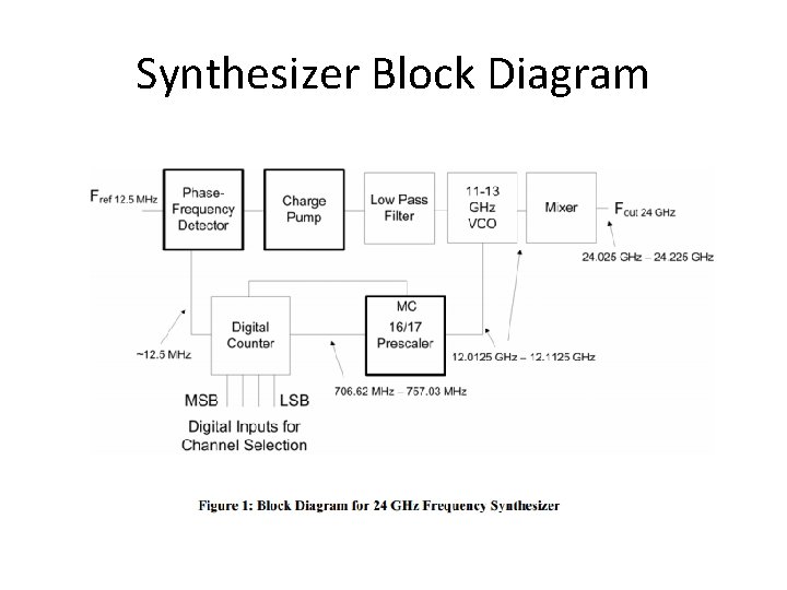
Synthesizer Block Diagram

Part 02: Initial Efforts • LTSPICE with MOSIS 180 n. M SPICE model

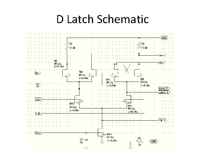
D Latch Schematic

D Flip Flop Schematic

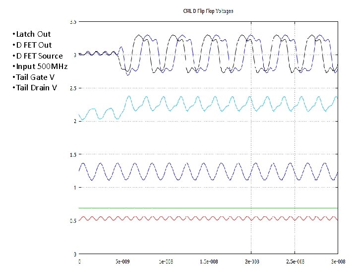
• Latch Out • D FET Source • Input 500 MHz • Tail Gate V • Tail Drain V

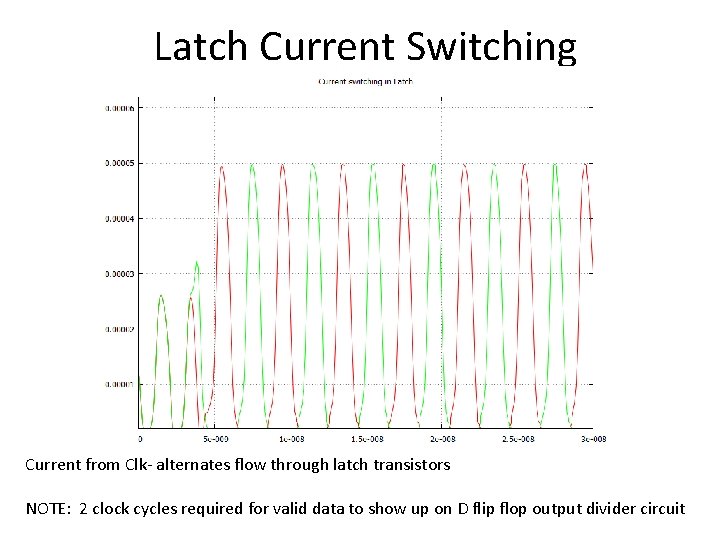
Latch Current Switching Current from Clk- alternates flow through latch transistors NOTE: 2 clock cycles required for valid data to show up on D flip flop output divider circuit

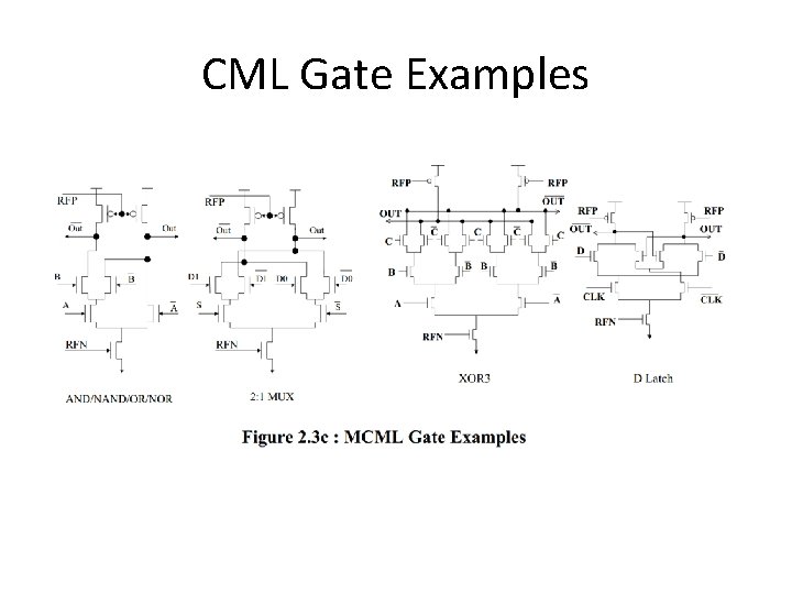
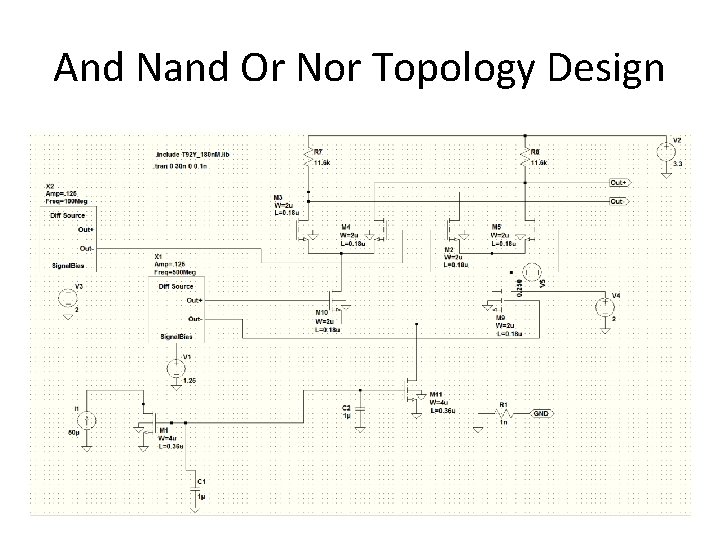
CML Gate Examples

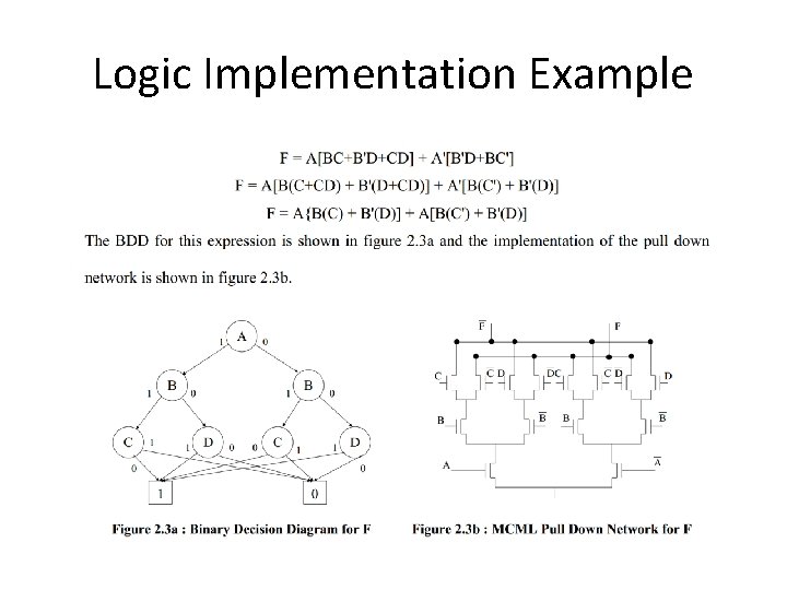
Logic Implementation Example

And Nand Or Nor Topology Design

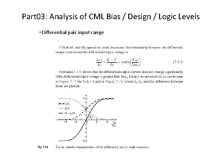
Part 03: Analysis of CML Bias / Design / Logic Levels • Differential pair input range

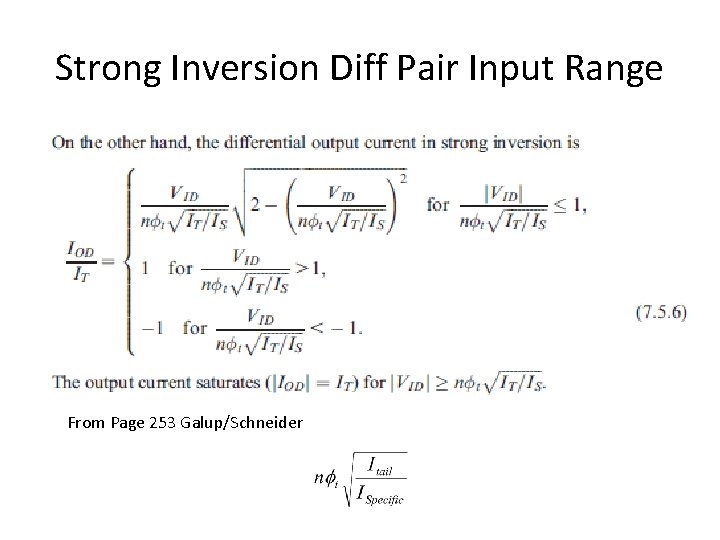
Strong Inversion Diff Pair Input Range From Page 253 Galup/Schneider

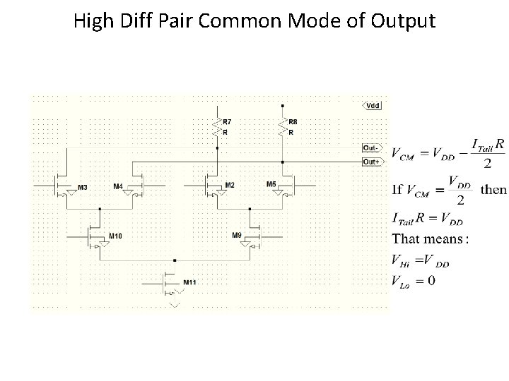
High Diff Pair Common Mode of Output

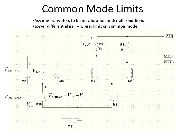
Common Mode Limits • Assume transistors to be in saturation under all conditions • Lower differential pair – Upper limit on common mode

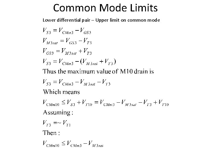
Common Mode Limits Lower differential pair – Upper limit on common mode

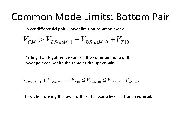
Common Mode Limits: Bottom Pair Lower differential pair – lower limit on common mode Putting it all together we can see the common mode of the lower pair can not be the same as the upper pair Thus when driving the lower differential pair a level shifter is required.

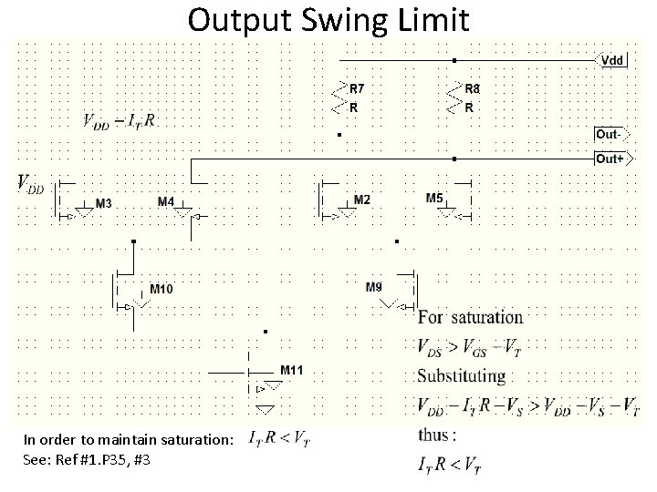
Output Swing Limit In order to maintain saturation: See: Ref #1. P 35, #3

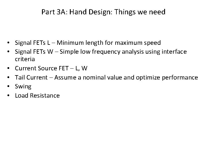
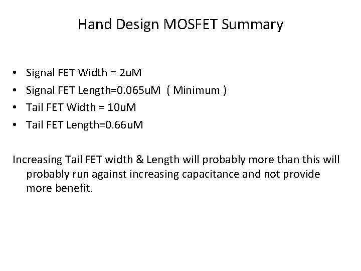
Part 3 A: Hand Design: Things we need • Signal FETs L – Minimum length for maximum speed • Signal FETs W – Simple low frequency analysis using interface criteria • Current Source FET – L, W • Tail Current – Assume a nominal value and optimize performance • Swing • Load Resistance

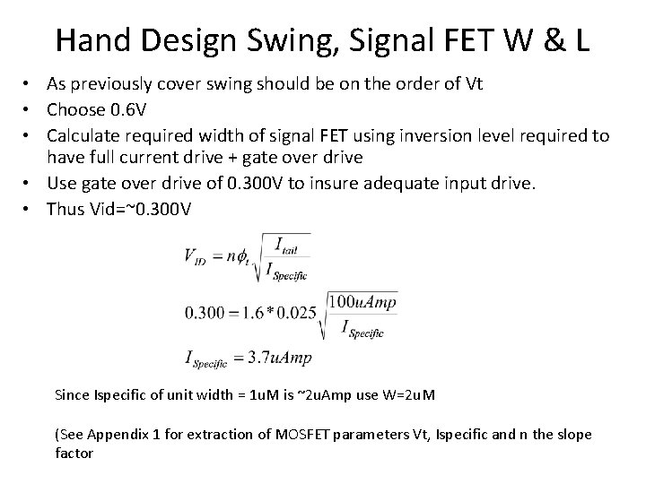
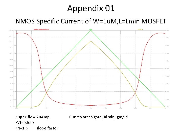
Hand Design Swing, Signal FET W & L • As previously cover swing should be on the order of Vt • Choose 0. 6 V • Calculate required width of signal FET using inversion level required to have full current drive + gate over drive • Use gate over drive of 0. 300 V to insure adequate input drive. • Thus Vid=~0. 300 V Since Ispecific of unit width = 1 u. M is ~2 u. Amp use W=2 u. M (See Appendix 1 for extraction of MOSFET parameters Vt, Ispecific and n the slope factor

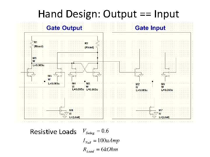
Hand Design: Output == Input Resistive Loads

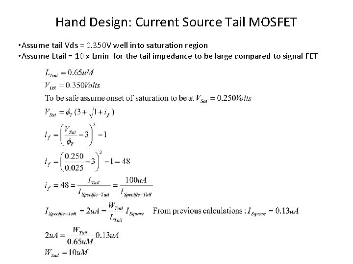
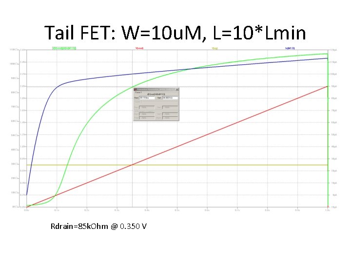
Hand Design: Current Source Tail MOSFET • Assume tail Vds = 0. 350 V well into saturation region • Assume Ltail = 10 x Lmin for the tail impedance to be large compared to signal FET

Hand Design MOSFET Summary • • Signal FET Width = 2 u. M Signal FET Length=0. 065 u. M ( Minimum ) Tail FET Width = 10 u. M Tail FET Length=0. 66 u. M Increasing Tail FET width & Length will probably more than this will probably run against increasing capacitance and not provide more benefit.

Part 04: Simulation: D Flip Flop in IBM 65 nm • MOSIS: IBM-Fishkill 65 nm SPICE FILE

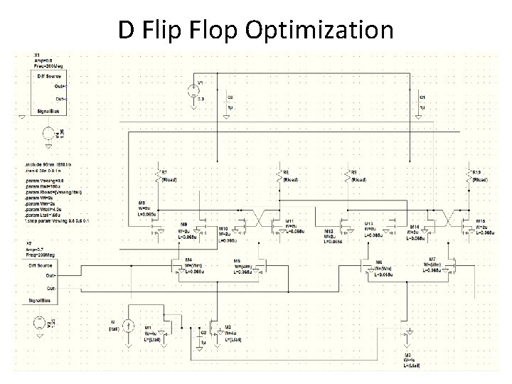
D Flip Flop Optimization

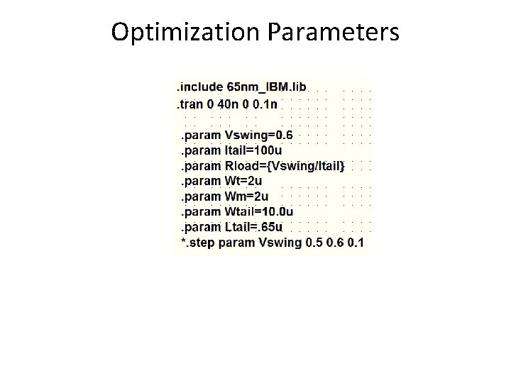
Optimization Parameters

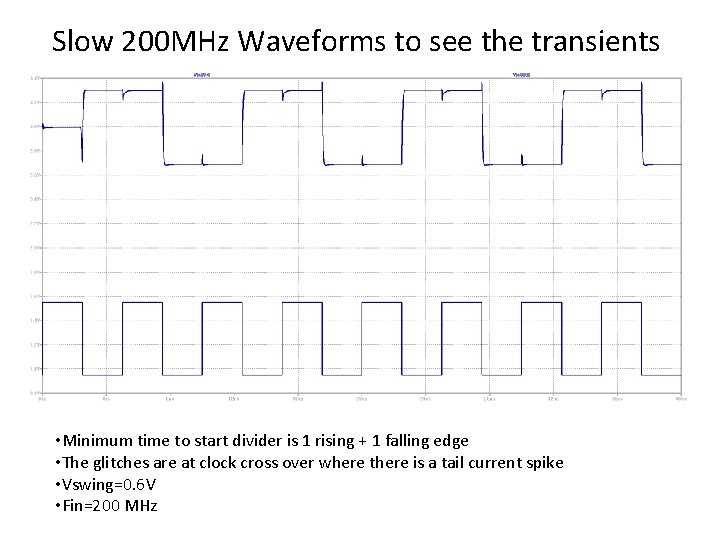
Slow 200 MHz Waveforms to see the transients • Minimum time to start divider is 1 rising + 1 falling edge • The glitches are at clock cross over where there is a tail current spike • Vswing=0. 6 V • Fin=200 MHz

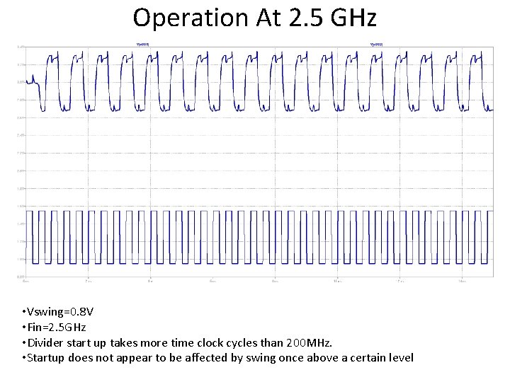
Operation At 2. 5 GHz • Vswing=0. 8 V • Fin=2. 5 GHz • Divider start up takes more time clock cycles than 200 MHz. • Startup does not appear to be affected by swing once above a certain level

D Flip Flop Optimization • • Power is independent of frequency Power is independent of swing Power consumption = Vdd * Itail * Num. Tails Output waveform had better rise time for lower swing – However did not work when used with higher assembly • Changes in signal MOSFET widths resulted in small changes in rise time – Going to Wt = Wm = 1 u might be slightly better. – Much narrower or much wider resulted in worse rise times • Works over -40 to +80 C

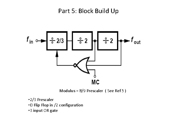
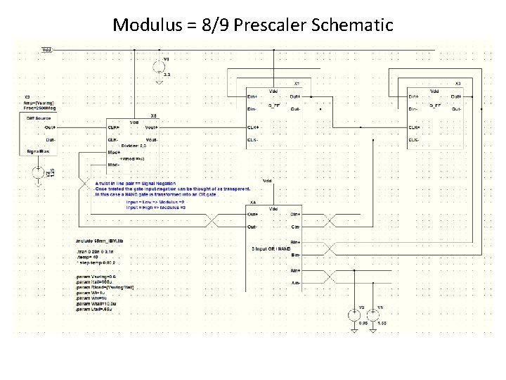
Part 5: Block Build Up Modulus = 8/9 Prescaler ( See Ref 5 ) • 2/3 Prescaler • D Flip Flop in /2 configuration • 3 input OR gate

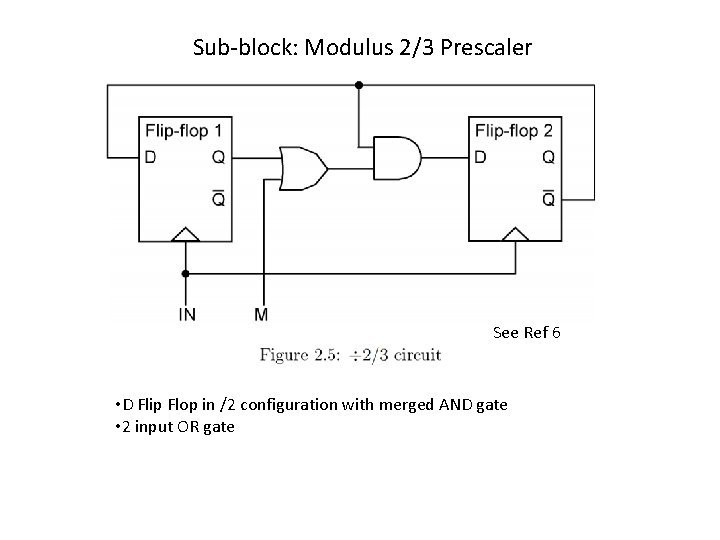
Sub-block: Modulus 2/3 Prescaler See Ref 6 • D Flip Flop in /2 configuration with merged AND gate • 2 input OR gate

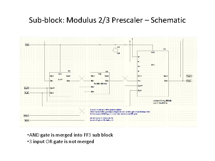
Sub-block: Modulus 2/3 Prescaler – Schematic • AND gate is merged into FF 3 sub block • 3 input OR gate is not merged

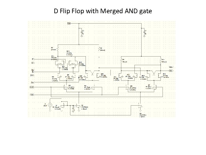
D Flip Flop with Merged AND gate

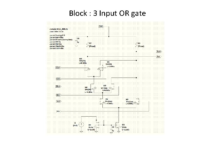
Block : 3 Input OR gate

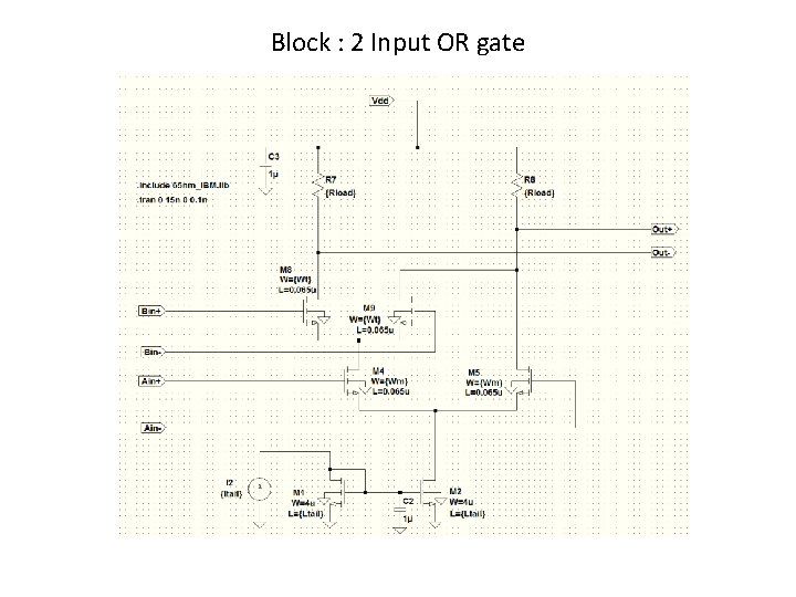
Block : 2 Input OR gate

Modulus = 8/9 Prescaler Schematic

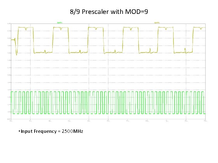
8/9 Prescaler with MOD=9 • Input Frequency = 2500 MHz

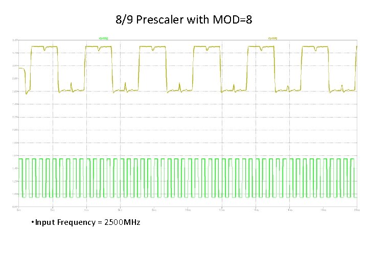
8/9 Prescaler with MOD=8 • Input Frequency = 2500 MHz

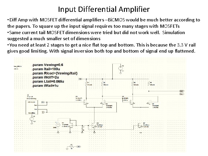
Input Differential Amplifier • Diff Amp with MOSFET differential amplifiers –Bi. CMOS would be much better according to the papers. To square up the input signal requires too many stages with MOSFETs • Same current tail MOSFET dimensions were tried but did not work well. Simulation suggested a much smaller set of dimensions • You need at least 2 stages to get a nice flat top and bottom. This is because the 3. 3 V rail gives good limiting. With signal inversion both top and bottom of signal end up flattened.

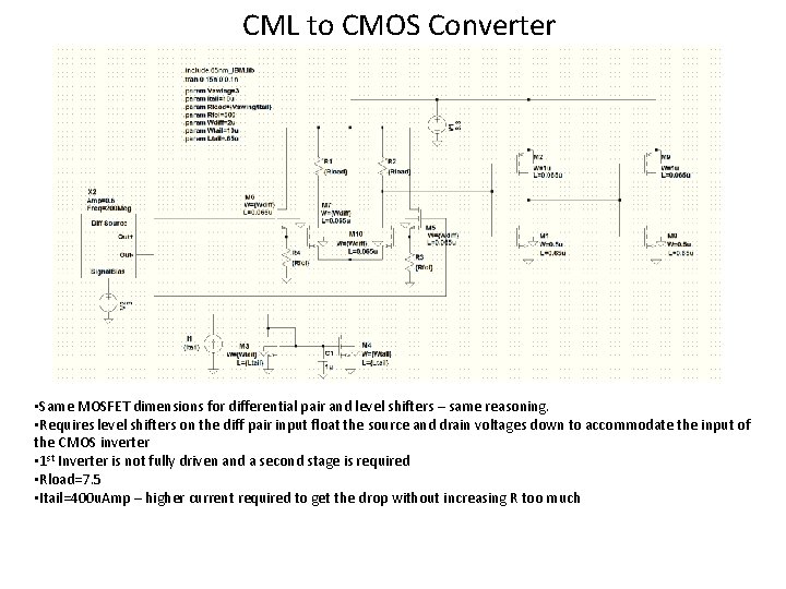
CML to CMOS Converter • Same MOSFET dimensions for differential pair and level shifters – same reasoning. • Requires level shifters on the diff pair input float the source and drain voltages down to accommodate the input of the CMOS inverter • 1 st Inverter is not fully driven and a second stage is required • Rload=7. 5 • Itail=400 u. Amp – higher current required to get the drop without increasing R too much

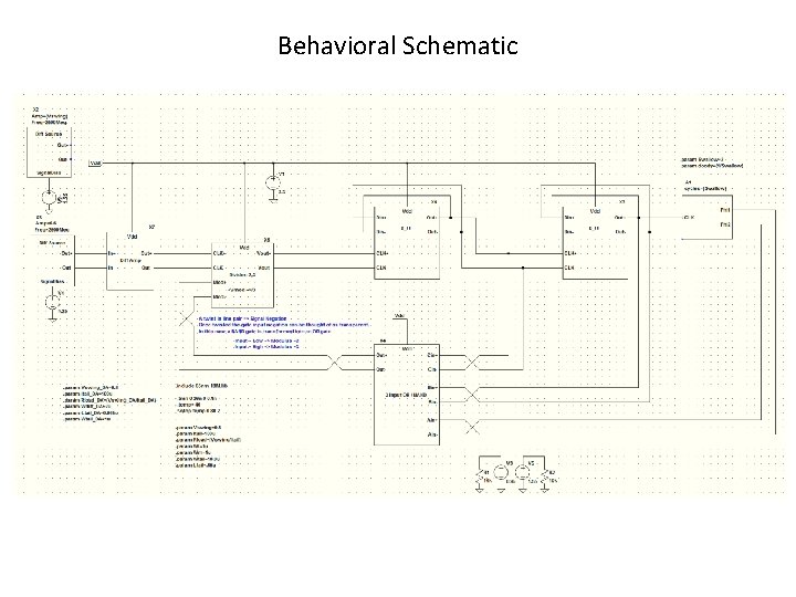
Behavioral Schematic

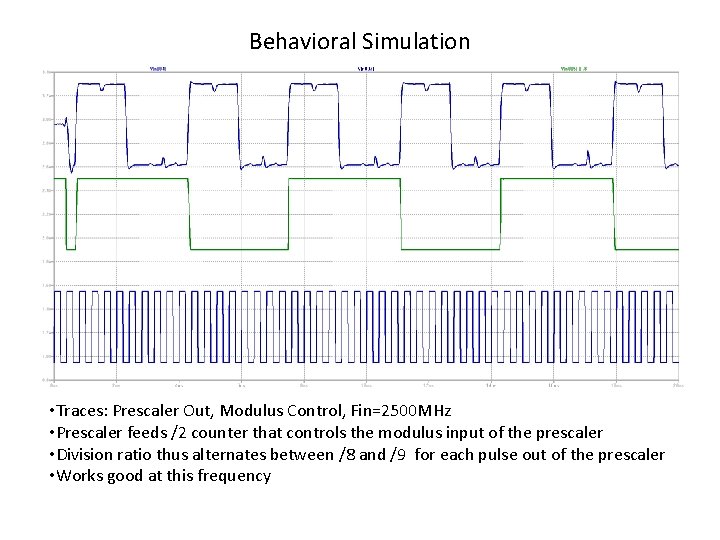
Behavioral Simulation • Traces: Prescaler Out, Modulus Control, Fin=2500 MHz • Prescaler feeds /2 counter that controls the modulus input of the prescaler • Division ratio thus alternates between /8 and /9 for each pulse out of the prescaler • Works good at this frequency

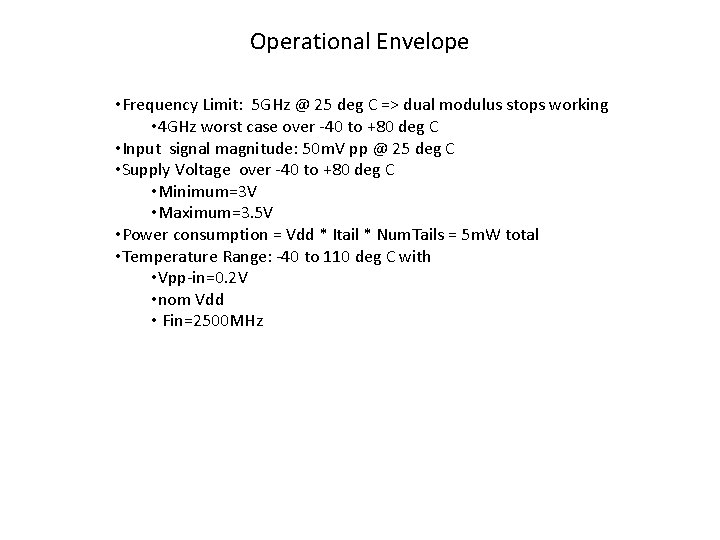
Operational Envelope • Frequency Limit: 5 GHz @ 25 deg C => dual modulus stops working • 4 GHz worst case over -40 to +80 deg C • Input signal magnitude: 50 m. V pp @ 25 deg C • Supply Voltage over -40 to +80 deg C • Minimum=3 V • Maximum=3. 5 V • Power consumption = Vdd * Itail * Num. Tails = 5 m. W total • Temperature Range: -40 to 110 deg C with • Vpp-in=0. 2 V • nom Vdd • Fin=2500 MHz

Appendix 01 NMOS Specific Current of W=1 u. M, L=Lmin MOSFET • Ispecific = 2 u. Amp • Vt=0. 650 • N=1. 6 slope factor Curves are: Vgate, Idrain, gm/Id

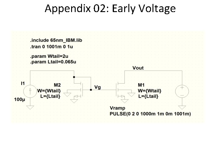
Appendix 02: Early Voltage

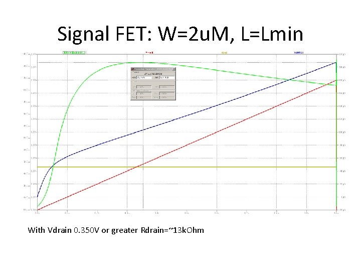
Signal FET: W=2 u. M, L=Lmin With Vdrain 0. 350 V or greater Rdrain=~13 k. Ohm

Tail FET: W=10 u. M, L=10*Lmin Rdrain=85 k. Ohm @ 0. 350 V

References 1. 2. 3. 4. 5. 6. High-Speed CMOS Dual-Modulus Prescalers for Frequency Synthesis by Ranganathan Desikachari An Analysis of MOS Current Mode Logic for Low Power and High Performance Digital Logic by Jason Musicer Video: lecture 6 - Current mode logic - Basic circuit design Nagendra Krishnapura - IIT Madras CMOS Analog Design Using All Region MOSFET Modeling : Page 253, 254 ( Galup & Schneider ) - Diff pair input range Frequency Dividers - Professor Jri Lee Design of a 5. 8 GHz Multi-Modulus - Prescaler Vidar Myklebust