Overview of the new CMS ECAL electronics Outline


- Slides: 27

Overview of the new CMS ECAL electronics Outline - The “TDR era” - The new architecture - Front-End Electronics - Off-Detector Electronics - Summary Colmar, September 12, 2002 Ph. BUSSON LLR Ecole polytechnique, Palaiseau 1

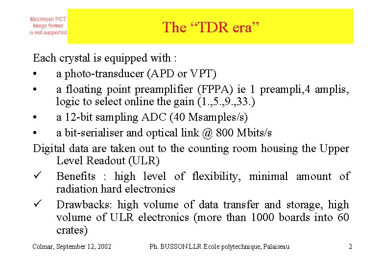
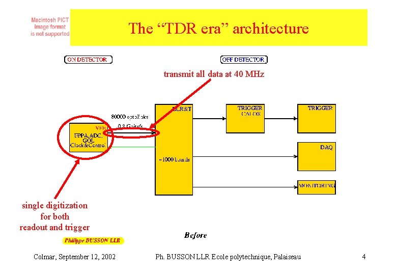
The “TDR era” Each crystal is equipped with : • a photo-transducer (APD or VPT) • a floating point preamplifier (FPPA) ie 1 preampli, 4 amplis, logic to select online the gain (1. , 5. , 9. , 33. ) • a 12 -bit sampling ADC (40 Msamples/s) • a bit-serialiser and optical link @ 800 Mbits/s Digital data are taken out to the counting room housing the Upper Level Readout (ULR) ü Benefits : high level of flexibility, minimal amount of radiation hard electronics ü Drawbacks: high volume of data transfer and storage, high volume of ULR electronics (more than 1000 boards into 60 crates) Colmar, September 12, 2002 Ph. BUSSON LLR Ecole polytechnique, Palaiseau 2

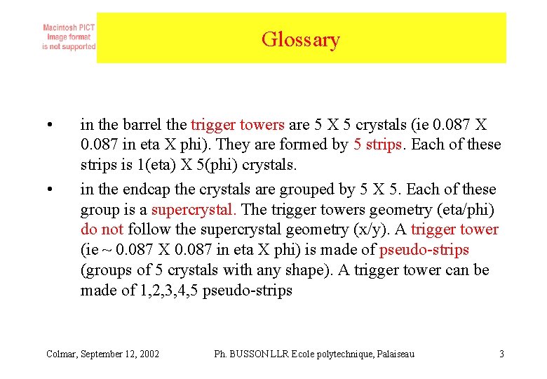
Glossary • • in the barrel the trigger towers are 5 X 5 crystals (ie 0. 087 X 0. 087 in eta X phi). They are formed by 5 strips. Each of these strips is 1(eta) X 5(phi) crystals. in the endcap the crystals are grouped by 5 X 5. Each of these group is a supercrystal. The trigger towers geometry (eta/phi) do not follow the supercrystal geometry (x/y). A trigger tower (ie ~ 0. 087 X 0. 087 in eta X phi) is made of pseudo-strips (groups of 5 crystals with any shape). A trigger tower can be made of 1, 2, 3, 4, 5 pseudo-strips Colmar, September 12, 2002 Ph. BUSSON LLR Ecole polytechnique, Palaiseau 3

The “TDR era” architecture transmit all data at 40 MHz single digitization for both readout and trigger Colmar, September 12, 2002 Ph. BUSSON LLR Ecole polytechnique, Palaiseau 4

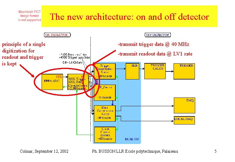
The new architecture: on and off detector principle of a single digitization for readout and trigger is kept Colmar, September 12, 2002 -transmit trigger data @ 40 MHz -transmit readout data @ LV 1 rate Ph. BUSSON LLR Ecole polytechnique, Palaiseau 5

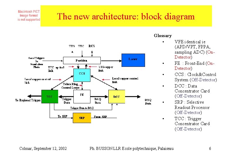
The new architecture: block diagram Glossary • VFE identical ie (APD/VPT, FPPA, sampling ADC) (On. Detector) • FE : Front-End (On. Detector) • CCS : Clock&Control System (Off-Detector) • DCC : Data Concentrator Card (Off-Detector) • SRP : Selective Readout Processor (Off-Detector) • TCC : Trigger Concentrator Card (Off-Detector) Colmar, September 12, 2002 Ph. BUSSON LLR Ecole polytechnique, Palaiseau 6

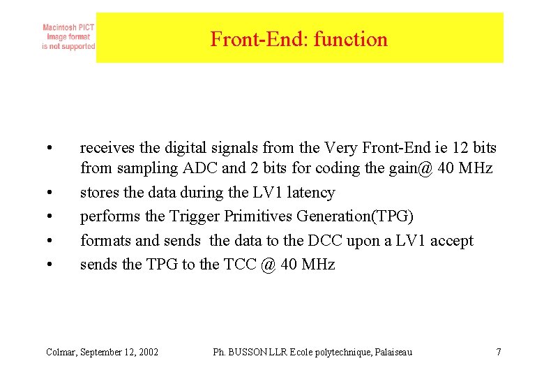
Front-End: function • • • receives the digital signals from the Very Front-End ie 12 bits from sampling ADC and 2 bits for coding the gain@ 40 MHz stores the data during the LV 1 latency performs the Trigger Primitives Generation(TPG) formats and sends the data to the DCC upon a LV 1 accept sends the TPG to the TCC @ 40 MHz Colmar, September 12, 2002 Ph. BUSSON LLR Ecole polytechnique, Palaiseau 7

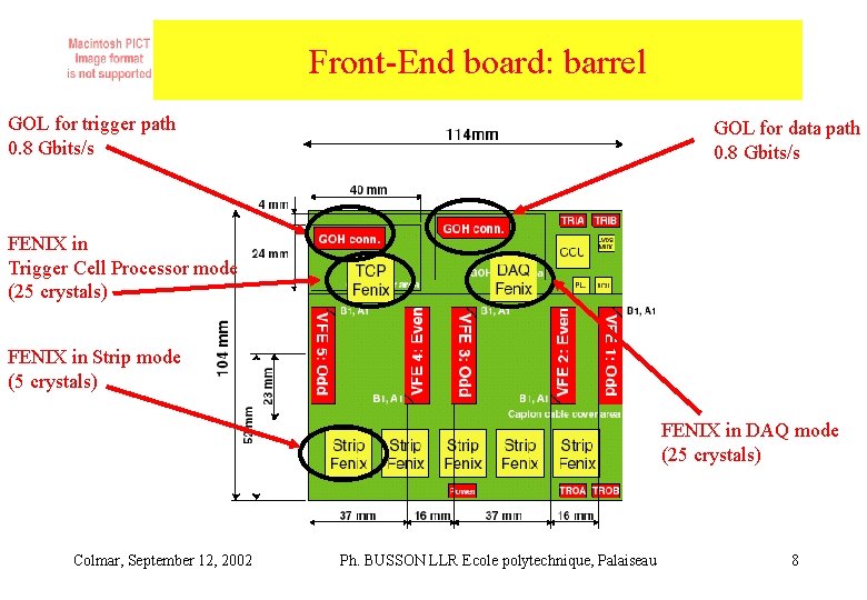
Front-End board: barrel GOL for trigger path 0. 8 Gbits/s GOL for data path 0. 8 Gbits/s FENIX in Trigger Cell Processor mode (25 crystals) FENIX in Strip mode (5 crystals) FENIX in DAQ mode (25 crystals) Colmar, September 12, 2002 Ph. BUSSON LLR Ecole polytechnique, Palaiseau 8

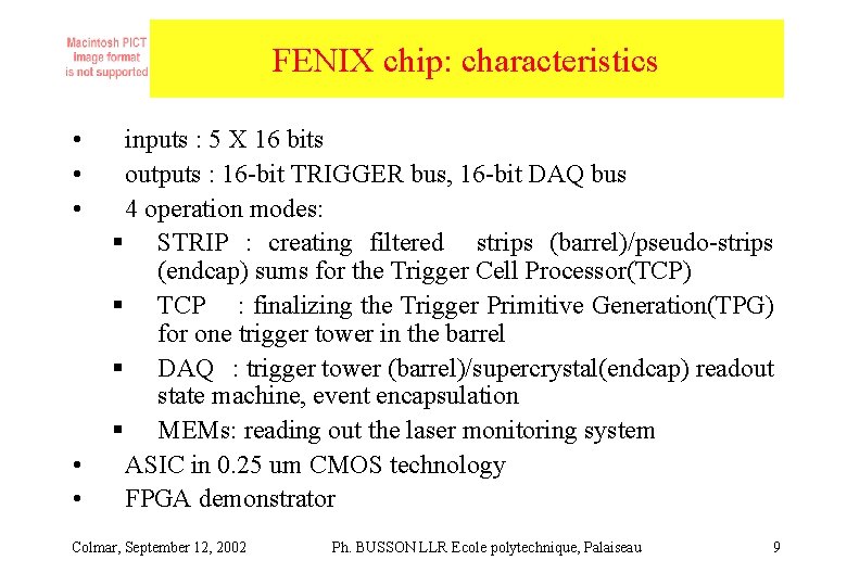
FENIX chip: characteristics • • • inputs : 5 X 16 bits outputs : 16 -bit TRIGGER bus, 16 -bit DAQ bus 4 operation modes: § STRIP : creating filtered strips (barrel)/pseudo-strips (endcap) sums for the Trigger Cell Processor(TCP) § TCP : finalizing the Trigger Primitive Generation(TPG) for one trigger tower in the barrel § DAQ : trigger tower (barrel)/supercrystal(endcap) readout state machine, event encapsulation § MEMs: reading out the laser monitoring system ASIC in 0. 25 um CMOS technology FPGA demonstrator Colmar, September 12, 2002 Ph. BUSSON LLR Ecole polytechnique, Palaiseau 9

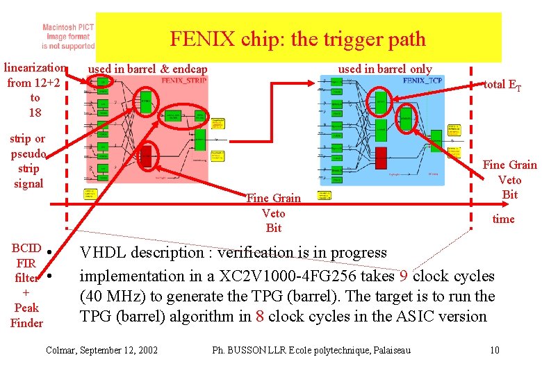
FENIX chip: the trigger path linearization from 12+2 to 18 used in barrel & endcap used in barrel only total ET strip or pseudo strip signal Fine Grain Veto Bit BCID • FIR filter • + Peak Finder Fine Grain Veto Bit time VHDL description : verification is in progress implementation in a XC 2 V 1000 -4 FG 256 takes 9 clock cycles (40 MHz) to generate the TPG (barrel). The target is to run the TPG (barrel) algorithm in 8 clock cycles in the ASIC version Colmar, September 12, 2002 Ph. BUSSON LLR Ecole polytechnique, Palaiseau 10

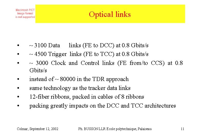
Optical links • • ~ 3100 Data links (FE to DCC) at 0. 8 Gbits/s ~ 4500 Trigger links (FE to TCC) at 0. 8 Gbits/s ~ 3000 Clock and Control links (FE from/to CCS) at 0. 8 Gbits/s instead of ~ 80000 in the TDR approach same technology as the tracker data links 12 -fiber ribbons, packed in cables of 8 ribbons packing greatly impacts on the DCC and TCC architectures Colmar, September 12, 2002 Ph. BUSSON LLR Ecole polytechnique, Palaiseau 11

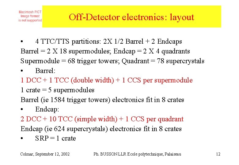
Off-Detector electronics: layout • 4 TTC/TTS partitions: 2 X 1/2 Barrel + 2 Endcaps Barrel = 2 X 18 supermodules; Endcap = 2 X 4 quadrants Supermodule = 68 trigger towers; Quadrant = 78 supercrystals • Barrel: 1 DCC + 1 TCC (double width) + 1 CCS per supermodule 1 crate = 5 supermodules Barrel (ie 1584 trigger towers) electronics fit in 8 crates • Endcap: 2 DCC + 10 TCC (simple width) + 1 CCS per quadrant Endcap (ie 624 supercrystals) electronics fit in 8 crates • SRP = 1 crate Colmar, September 12, 2002 Ph. BUSSON LLR Ecole polytechnique, Palaiseau 12

CCS: function • • interface to Trigger Control System (TCS) and Trigger Throttling System (TTS) distribution of clock and control signals DCC and TCC and front-end system fan-in the TTS signals from the DCC, TCC and SRP and transmission to TTS configuration of the Front-End system Colmar, September 12, 2002 Ph. BUSSON LLR Ecole polytechnique, Palaiseau 13

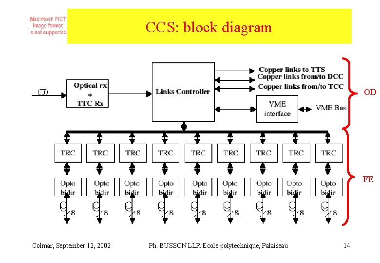
CCS: block diagram OD FE Colmar, September 12, 2002 Ph. BUSSON LLR Ecole polytechnique, Palaiseau 14

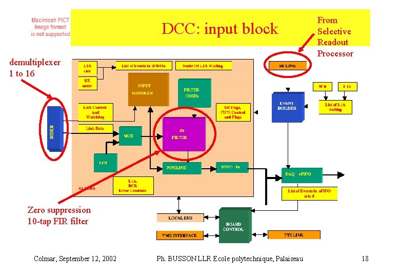
DCC: function • • • receives formatted digital data from the Front-End boards and TCC verifies integrity of the input event fragments reduces the data volume performing the zero suppression using the Selective Readout information provided by the SRP formats events transmits events to the global DAQ transmits monitoring and spying events to the local DAQ Colmar, September 12, 2002 Ph. BUSSON LLR Ecole polytechnique, Palaiseau 15

DCC: data volumes and data rates • • 38. 1 k. Bytes for input crystal event (10 time samples) 156 Bytes (barrel) or 300 Bytes (endcap) TCC event 2 k. Bytes average output event size data reduction factor 21 in average 200 Mbytes/s average output data rate 528 Mbytes/s maximum output data rate 32 events stored (maximum) Colmar, September 12, 2002 Ph. BUSSON LLR Ecole polytechnique, Palaiseau 16

DCC: block diagram moves i. FIFOs to o. FIFOs 68 inputs 2 inputs (monitoring) Receiver Block 2 channels each Colmar, September 12, 2002 to the DAQ Ph. BUSSON LLR Ecole polytechnique, Palaiseau 17

DCC: input block demultiplexer 1 to 16 From Selective Readout Processor Zero suppression 10 -tap FIR filter Colmar, September 12, 2002 Ph. BUSSON LLR Ecole polytechnique, Palaiseau 18

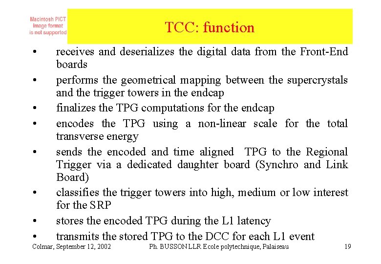
TCC: function • • receives and deserializes the digital data from the Front-End boards performs the geometrical mapping between the supercrystals and the trigger towers in the endcap finalizes the TPG computations for the endcap encodes the TPG using a non-linear scale for the total transverse energy sends the encoded and time aligned TPG to the Regional Trigger via a dedicated daughter board (Synchro and Link Board) classifies the trigger towers into high, medium or low interest for the SRP stores the encoded TPG during the L 1 latency transmits the stored TPG to the DCC for each L 1 event Colmar, September 12, 2002 Ph. BUSSON LLR Ecole polytechnique, Palaiseau 19

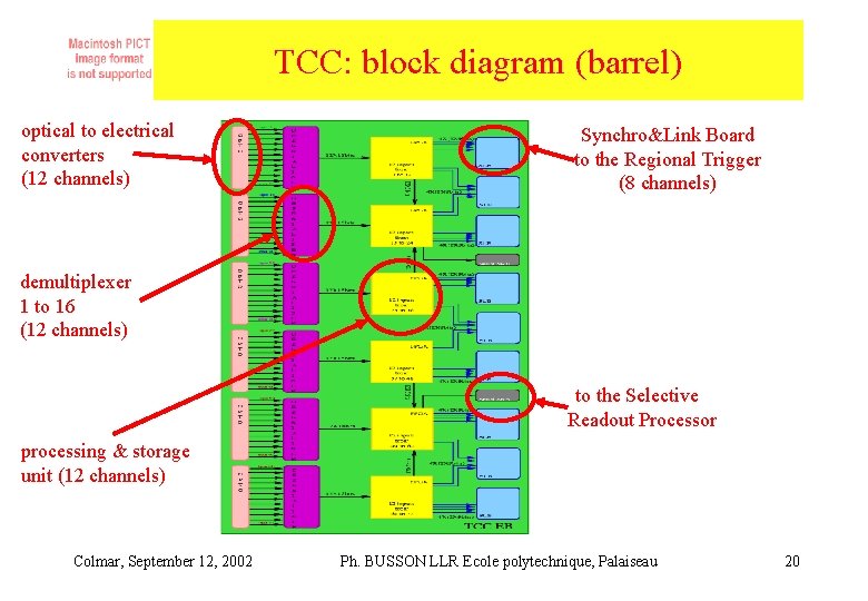
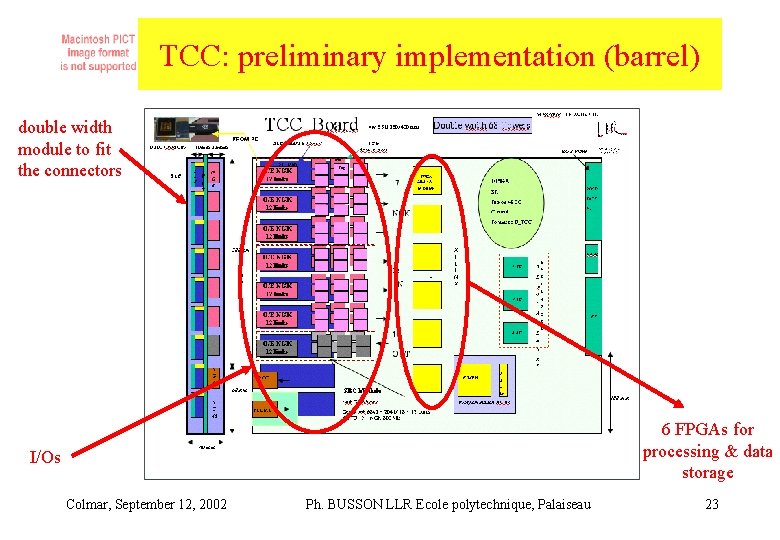
TCC: block diagram (barrel) optical to electrical converters (12 channels) Synchro&Link Board to the Regional Trigger (8 channels) demultiplexer 1 to 16 (12 channels) to the Selective Readout Processor processing & storage unit (12 channels) Colmar, September 12, 2002 Ph. BUSSON LLR Ecole polytechnique, Palaiseau 20

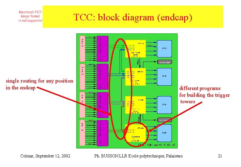
TCC: block diagram (endcap) single routing for any position in the endcap Colmar, September 12, 2002 different programs for building the trigger towers Ph. BUSSON LLR Ecole polytechnique, Palaiseau 21

SLB: block diagram 4 channels 2 Gbits/s ie 8 trigger towers to the Regional Trigger - build online histogram for survey of the LHC bunch crossings structure - align the channels BC 0 40. 08 to 120. 24 MHz Colmar, September 12, 2002 Ph. BUSSON LLR Ecole polytechnique, Palaiseau 22

TCC: preliminary implementation (barrel) double width module to fit the connectors 6 FPGAs for processing & data storage I/Os Colmar, September 12, 2002 Ph. BUSSON LLR Ecole polytechnique, Palaiseau 23

Selective Readout Processor: function • • selects dynamically (L 1 rate) the meaningful ECAL information which is spread in ~1. 5 Mbytes (ie number of crystals X 10 samples X 2 bytes) performs suppression in order to reduce the ECAL data volume (ie crystals and trigger towers data) to ~100 k. Bytes/event (average) Colmar, September 12, 2002 Ph. BUSSON LLR Ecole polytechnique, Palaiseau 24

Selective Readout Processor: principles • • • organizes the readout using “readout towers” of 25 crystals (barrel: trigger towers, endcap: supercrystals) classifies the readout towers in term of total transverse energy (high, medium or low interest) establishes correspondence between classification and “readout state” (no reading, full reading, reading with Zero Suppression) Colmar, September 12, 2002 Ph. BUSSON LLR Ecole polytechnique, Palaiseau 25

Selective Readout Processor: 2 possible implementations • • TCC produces the classification @ 40 MHz, SRP produces the readout states during the L 1 latency requiring a very high (80 GBytes/s) transfer rate between TCC and SRP. TCC produces the classification @ L 1 rate (100 k. Hz), SRP produces the readout states after the L 1 accept signal requiring extra buffering in TCC and DCC for data storage Colmar, September 12, 2002 Ph. BUSSON LLR Ecole polytechnique, Palaiseau 26

Summary • • • New ECAL electronics architecture has been presented Major reduction (~40%) of the total cost of the system with exactly the same functionality as described in the TDR Design of a new radiation hard ASIC (FENIX chip) in 0. 25 um is already started Reduced number of data links between the On and Off Detector electronics using the same technology as the tracker (re)Design of the less costly Off-Detector electronics has recently started Colmar, September 12, 2002 Ph. BUSSON LLR Ecole polytechnique, Palaiseau 27