Overview of Electrostatic Recommendations in Updated E 78
- Slides: 24

Overview of Electrostatic Recommendations in Updated E 78, E 129, and ITRS 2005 Arnold Steinman M. S. E. E. Chief Applied Technologist MKS, Ion Systems Leader – SEMI ESD Task Force ESDA Certified ESD Program Manager NARTE Certified ESD Engineer asteinman@ion. com Jan 1, 2006 Event, Venue information

Outline • Problems caused by static charge • Static Control Basics – Grounding and Ionization • Static control requirements – Semiconductor Industry Standards – SEMI E 78 – Static control in Production Equipment – SEMI E 129 – Controlling Static Charge in the Factory – International Technology Roadmap for Semiconductors • ANSI ESD S 20. 20 – Static Control Program • Conclusions 2

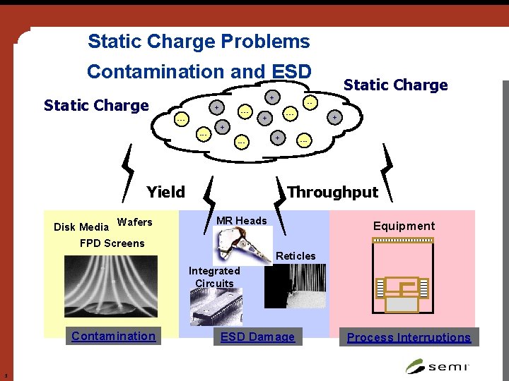
Static Charge Problems Contamination and ESD + Static Charge + ----- + + + --- Yield Disk Media Wafers Static Charge + --- Throughput MR Heads Equipment FPD Screens Reticles Integrated Circuits Contamination 3 ESD Damage Process Interruptions

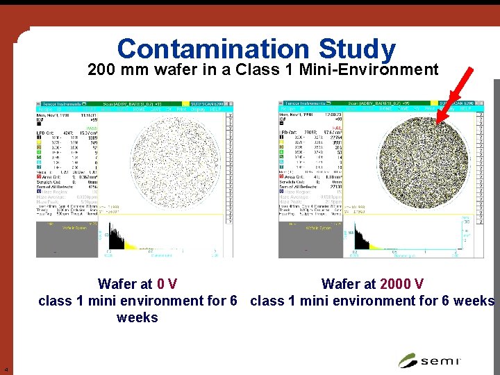
Contamination Study 200 mm wafer in a Class 1 Mini-Environment Wafer at 0 V Wafer at 2000 V class 1 mini environment for 6 weeks 4

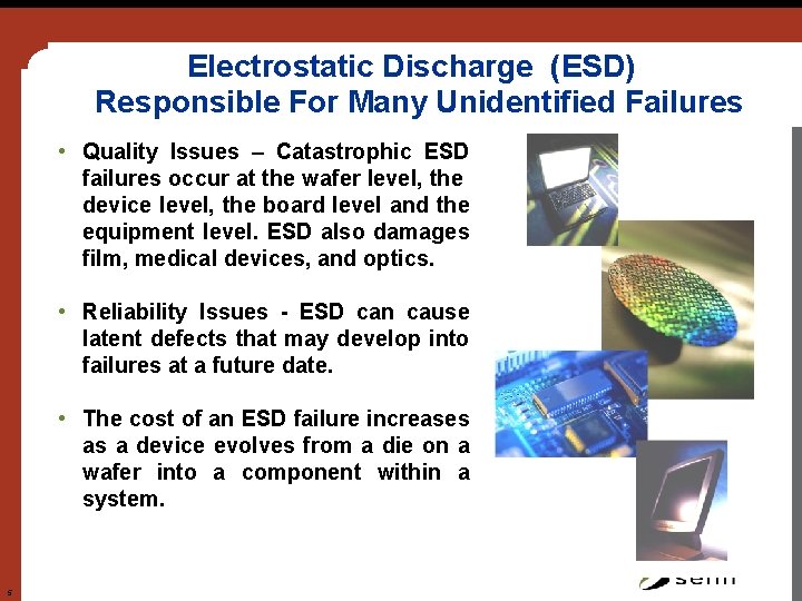
Electrostatic Discharge (ESD) Responsible For Many Unidentified Failures • Quality Issues – Catastrophic ESD failures occur at the wafer level, the device level, the board level and the equipment level. ESD also damages film, medical devices, and optics. • Reliability Issues - ESD can cause latent defects that may develop into failures at a future date. • The cost of an ESD failure increases as a device evolves from a die on a wafer into a component within a system. 5

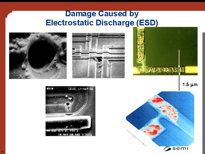
Damage Caused by Electrostatic Discharge (ESD) 1. 5 m 6

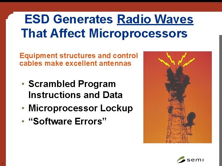
ESD Generates Radio Waves That Affect Microprocessors Equipment structures and control cables make excellent antennas • Scrambled Program Instructions and Data • Microprocessor Lockup • “Software Errors” 7

The Basics • Static Charge Generation – Triboelectric Charging – Induction Charging • Static Charge Control – Personnel Grounding – Worksurface Grounding – Static Dissipative Materials • Insulators 8

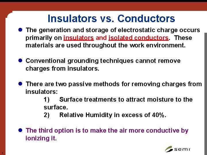
Insulators vs. Conductors l The generation and storage of electrostatic charge occurs primarily on insulators and isolated conductors. These materials are used throughout the work environment. l Conventional grounding techniques cannot remove charges from insulators. l There are two passive methods for removing charges from insulators: 1) Surface treatments to attract moisture to the surface. 2) Relative Humidity in excess of 40%. l The third option is to make the air more conductive by ionizing it. 9

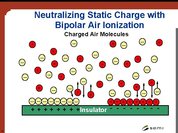
Neutralizing Static Charge with Bipolar Air Ionization Charged Air Molecules --- + + + --- --- + ----- + --- --- + + ----- + + + --- --- + + --- --+ + + +Insulator - - - - 10

International Technology Roadmap for Semiconductors (ITRS) 2005 Factory Integration Chapter Static Control – pg 35 download - www. sematech. org 11

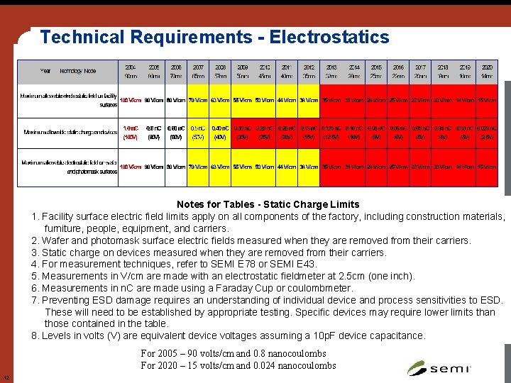
Technical Requirements - Electrostatics Notes for Tables - Static Charge Limits 1. Facility surface electric field limits apply on all components of the factory, including construction materials, furniture, people, equipment, and carriers. 2. Wafer and photomask surface electric fields measured when they are removed from their carriers. 3. Static charge on devices measured when they are removed from their carriers. 4. For measurement techniques, refer to SEMI E 78 or SEMI E 43. 5. Measurements in V/cm are made with an electrostatic fieldmeter at 2. 5 cm (one inch). 6. Measurements in n. C are made using a Faraday Cup or coulombmeter. 7. Preventing ESD damage requires an understanding of individual device and process sensitivities to ESD. These will need to be established by appropriate testing. Specific devices may require lower limits than those contained in the table. 8. Levels in volts (V) are equivalent device voltages assuming a 10 p. F device capacitance. For 2005 – 90 volts/cm and 0. 8 nanocoulombs For 2020 – 15 volts/cm and 0. 024 nanocoulombs 12

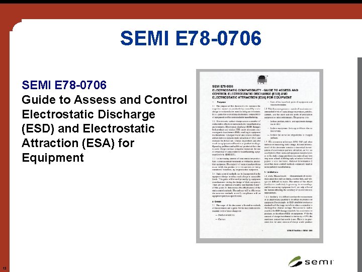
SEMI E 78 -0706 Guide to Assess and Control Electrostatic Discharge (ESD) and Electrostatic Attraction (ESA) for Equipment 13

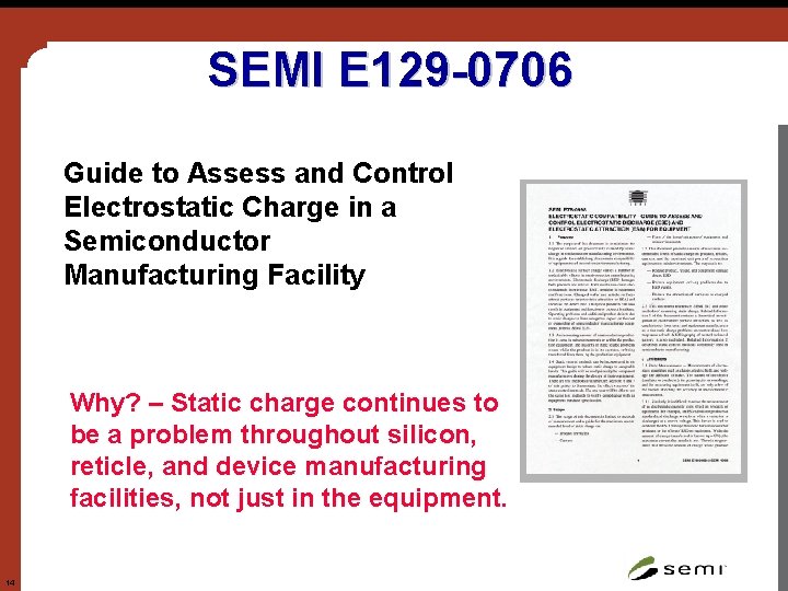
SEMI E 129 -0706 Guide to Assess and Control Electrostatic Charge in a Semiconductor Manufacturing Facility Why? – Static charge continues to be a problem throughout silicon, reticle, and device manufacturing facilities, not just in the equipment. 14

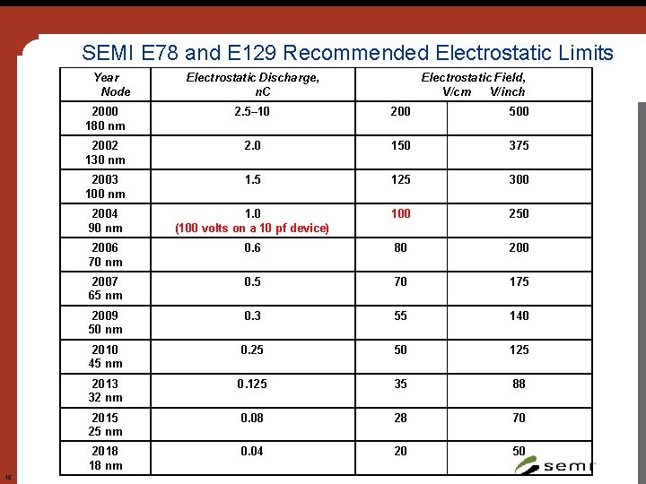
SEMI E 78 and E 129 Recommended Electrostatic Limits Year Node 15 Electrostatic Discharge, n. C Electrostatic Field, V/cm V/inch 2000 180 nm 2. 5– 10 200 500 2002 130 nm 2. 0 150 375 2003 100 nm 1. 5 125 300 2004 90 nm 1. 0 (100 volts on a 10 pf device) 100 250 2006 70 nm 0. 6 80 2007 65 nm 0. 5 70 175 2009 50 nm 0. 3 55 140 2010 45 nm 0. 25 50 125 2013 32 nm 0. 125 35 88 2015 25 nm 0. 08 28 70 2018 18 nm 0. 04 20 50

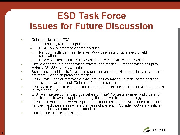
ESD Task Force Issues for Future Discussion • • 16 Relationship to the ITRS – Technology Node designations – DRAM vs. Microprocessor table values – Random faults per mask level vs. PWP used in allowable electric field calculations – DRAM ½ pitch vs. MPU/ASIC Metal 1 ½ pitch Different charge levels for devices, wafers, and reticles (10 pf for devices, 220 pf for wafers, 70 -100 pf for photomasks Scale electric field limits for particle deposition based on killer particle size. Now they are mostly based on protecting reticles. E 78 - Review and/or remove the “background information” in many of the sections and include in an Appendix/Related Information section. E 78 - Write clear instructions on the use of Table 1 in Section 12. (see 4 step process in Comment KT-3) E 78 - Rewrite Section 9 to include details on type(s) of tests, number and type(s) of samples, etc. to avoid supplier/user negotiations over test methodology E 129 – Differentiate between requirements for areas where devices and reticles are handled, and those areas where they are not present. In/outside FOUPs and reticle carriers, minienvironments, equipment, etc. Reticle electrostatic field issues.

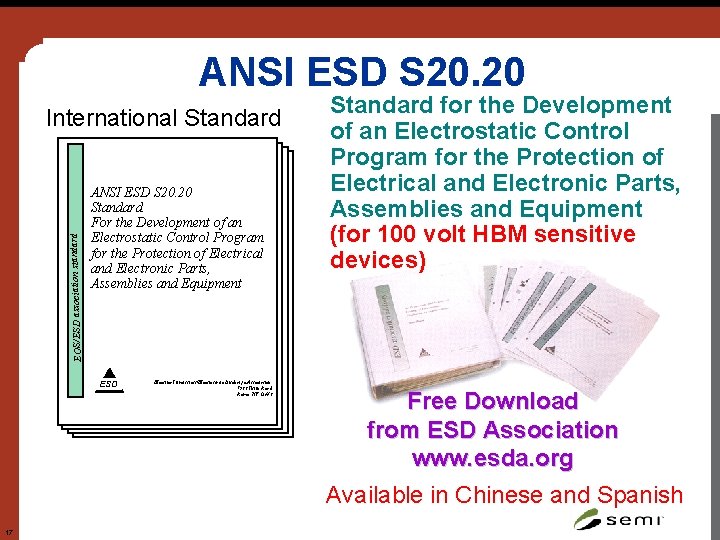
ANSI ESD S 20. 20 EOS/ESD association standard International Standard ANSI ESD S 20. 20 Standard For the Development of an Electrostatic Control Program for the Protection of Electrical and Electronic Parts, Assemblies and Equipment ESD 17 Electrical Overstress/Electrostatic Discharge Association 7900 Turin Road Rome, NY 13440 Standard for the Development of an Electrostatic Control Program for the Protection of Electrical and Electronic Parts, Assemblies and Equipment (for 100 volt HBM sensitive devices) Free Download from ESD Association www. esda. org Available in Chinese and Spanish

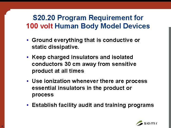
S 20. 20 Program Requirement for 100 volt Human Body Model Devices • Ground everything that is conductive or static dissipative. • Keep charged insulators and isolated conductors 30 cm away from sensitive product at all times • Use ionization whenever there are process essential insulators in the product or process • Establish facility audit and training programs 18

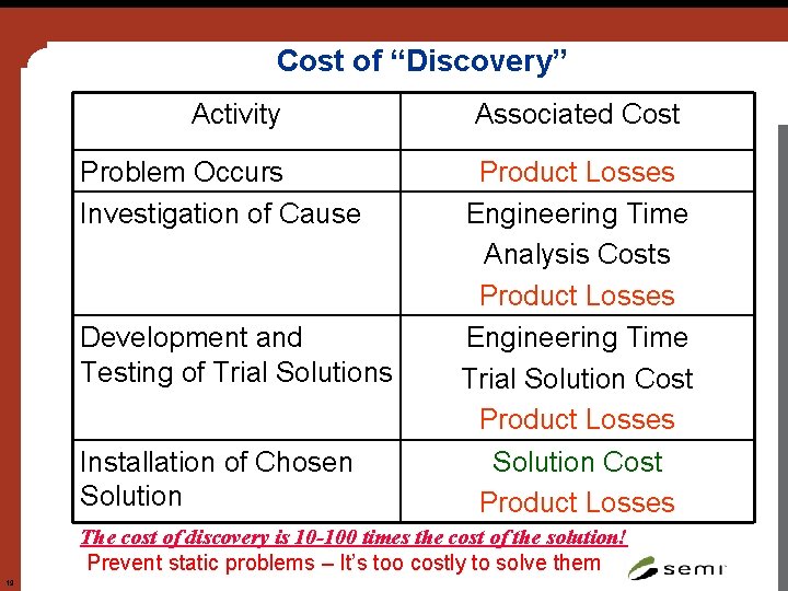
Cost of “Discovery” Activity Problem Occurs Investigation of Cause Development and Testing of Trial Solutions Installation of Chosen Solution Associated Cost Product Losses Engineering Time Analysis Costs Product Losses Engineering Time Trial Solution Cost Product Losses The cost of discovery is 10 -100 times the cost of the solution! Prevent static problems – It’s too costly to solve them 19

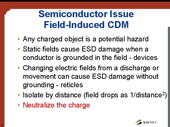
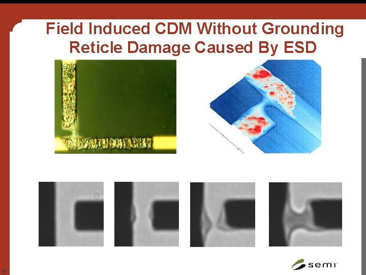
Semiconductor Issue Field-Induced CDM • Any charged object is a potential hazard • Static fields cause ESD damage when a conductor is grounded in the field - devices • Changing electric fields from a discharge or movement can cause ESD damage without grounding - reticles • Isolate by distance (field drops as 1/distance 2) • Neutralize the charge 20

Field Induced CDM Without Grounding Reticle Damage Caused By ESD 21

New Customer Requirements • Documented Static Control Program • Maintain Static Levels in the whole factory less than 100 volts – ANSI ESD S 20. 20 – 100 volts HBM – SEMI E 129 – 100 volts CDM for a 10 pf IC (1 n. C) – ITRS for 2004 – 100 volts CDM for a 10 pf IC (1 n. C) • Required for New Business 22

Achieving the 100 volt Customer Requirement • Ground all conductors - 0 volts • Reduce the charge on insulators and isolated conductors with ionizers – less than 100 volts/inch • Educate the customer – 100 volts/inch on a Fieldmeter has nothing to do with a 100 volt device ESD sensitivity 23

Conclusions • Static charge issues will not go away. Solving them becomes more important with technology change. • A complete static control program requires grounding, proper material selection, and ionization to control charge on insulators. Use ANSI ESD S 20. • SEMI E 78 and E 129 address static control requirements for the semiconductor factory of the future, synchronizing with ITRS 2005. These documents will be harmonized and updated every 2 years • The discussion of the many issues concerning static charge control in semiconductors is continuing. Please join the ESD Task Force to be part of that discussion. Static control is not an option! 24