Overview and Status of ATLAS Pixel Detector Waruna
- Slides: 16

Overview and Status of ATLAS Pixel Detector Waruna Fernando The Ohio State University on behalf of the ATLAS Pixel Collaboration

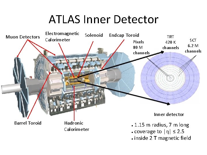
ATLAS Inner Detector Muon Detectors Electromagnetic Calorimeter Solenoid Endcap Toroid Pixels 80 M channels TRT 420 K channels SCT 6. 2 M channels Inner detector Barrel Toroid Hadronic Calorimeter 1. 15 m radius, 7 m long ● coverage to |η| ≤ 2. 5 ● inside 2 T magnetic field ●

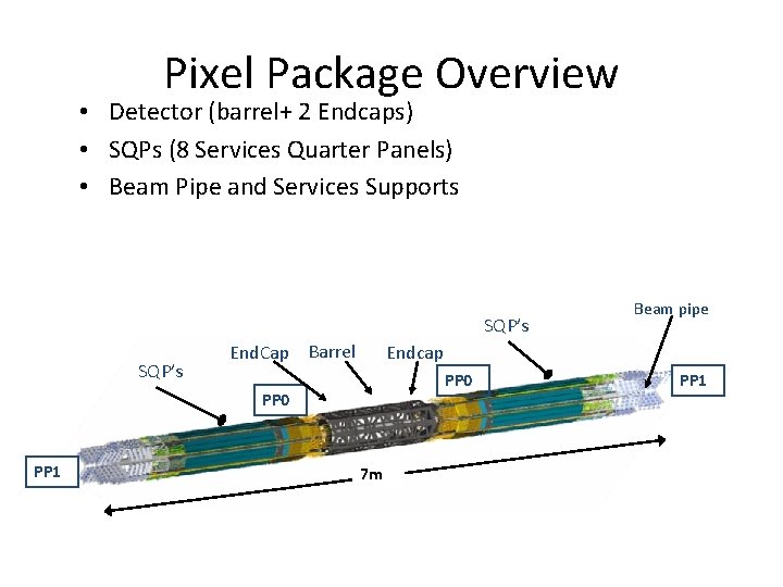
Pixel Package Overview • Detector (barrel+ 2 Endcaps) • SQPs (8 Services Quarter Panels) • Beam Pipe and Services Supports SQP’s End. Cap Barrel Endcap PP 0 PP 1 Beam pipe 7 m PP 1

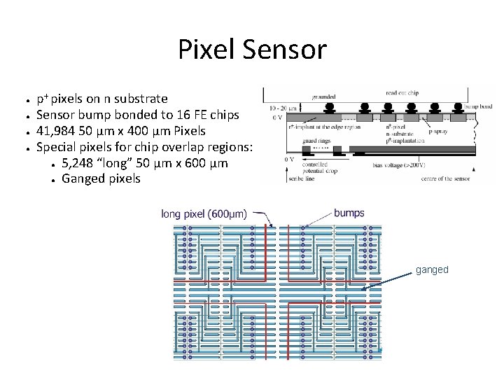
Pixel Sensor ● ● p+ pixels on n substrate Sensor bump bonded to 16 FE chips 41, 984 50 μm x 400 μm Pixels Special pixels for chip overlap regions: ● 5, 248 “long” 50 μm x 600 μm ● Ganged pixels ganged

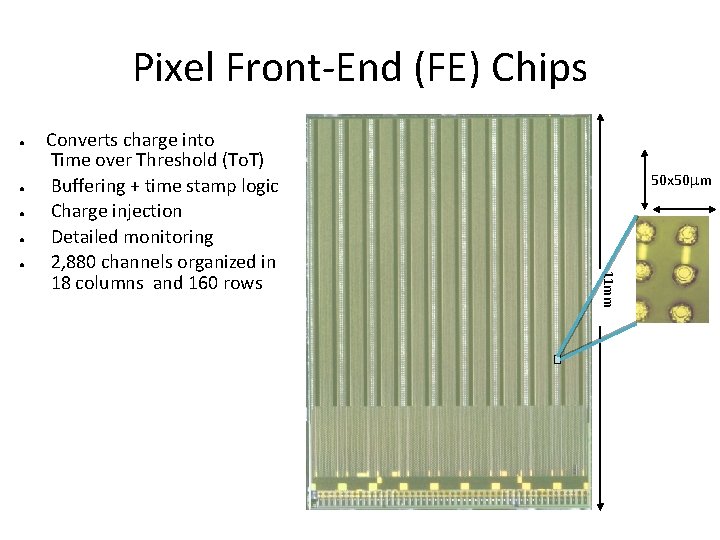
Pixel Front-End (FE) Chips ● ● ● 50 x 50 m 11 mm Converts charge into Time over Threshold (To. T) Buffering + time stamp logic Charge injection Detailed monitoring 2, 880 channels organized in 18 columns and 160 rows

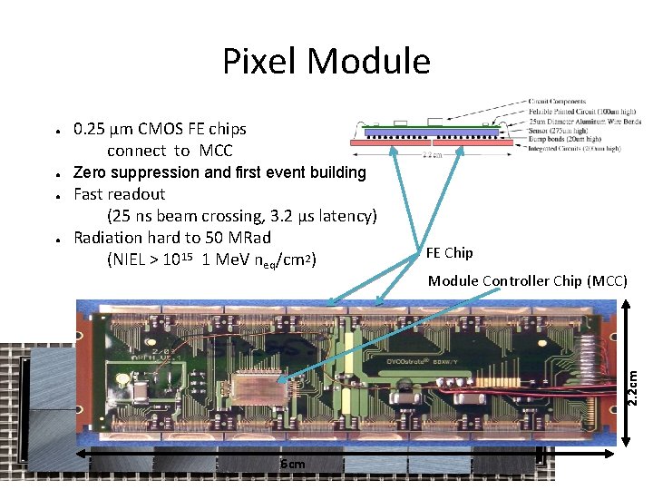
Pixel Module ● ● ● 0. 25 μm CMOS FE chips connect to MCC Zero suppression and first event building Fast readout (25 ns beam crossing, 3. 2 μs latency) Radiation hard to 50 MRad (NIEL > 1015 1 Me. V neq/cm 2) FE Chip Module Controller Chip (MCC) 2. 2 cm ● 6 cm

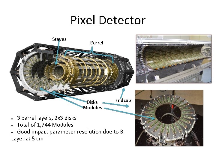
Pixel Detector Staves Barrel Disks Modules Endcap 3 barrel layers, 2 x 3 disks ● Total of 1, 744 Modules ● Good impact parameter resolution due to BLayer at 5 cm ●

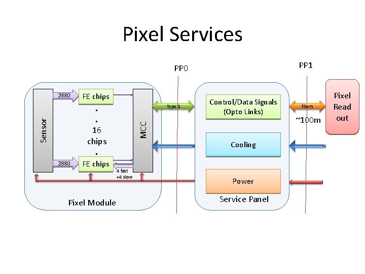
Pixel Services PP 1 PP 0 2880 FE chips Pixel Module Type 0 MCC Sensor . . 16 chips. Control/Data Signals (Opto Links) Cooling 4 fast +4 slow Power Service Panel fibers ~100 m Pixel Read out

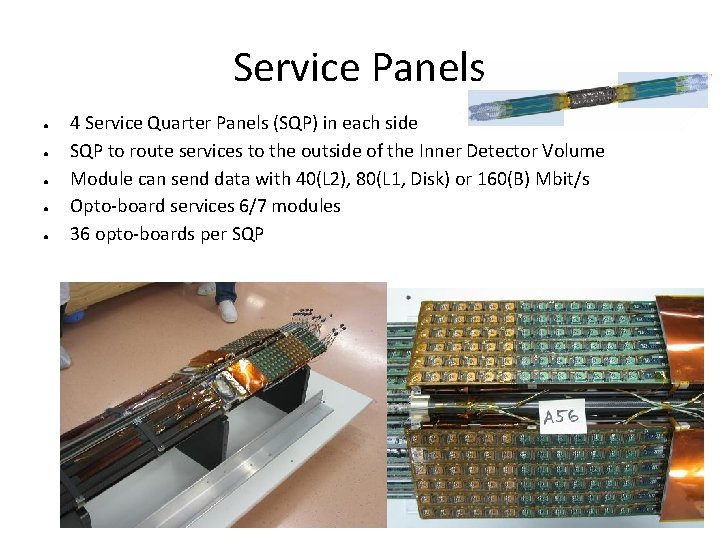
Service Panels ● ● ● 4 Service Quarter Panels (SQP) in each side SQP to route services to the outside of the Inner Detector Volume Module can send data with 40(L 2), 80(L 1, Disk) or 160(B) Mbit/s Opto-board services 6/7 modules 36 opto-boards per SQP

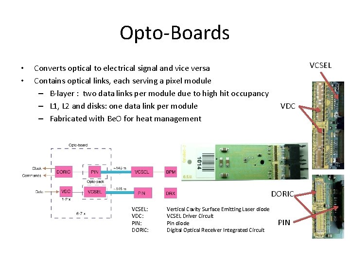
Opto-Boards • • Converts optical to electrical signal and vice versa Contains optical links, each serving a pixel module – B-layer : two data links per module due to high hit occupancy – L 1, L 2 and disks: one data link per module – Fabricated with Be. O for heat management VCSEL VDC DORIC VCSEL: VDC: PIN: DORIC: Vertical Cavity Surface Emitting Laser diode VCSEL Driver Circuit Pin diode Digital Optical Receiver Integrated Circuit PIN

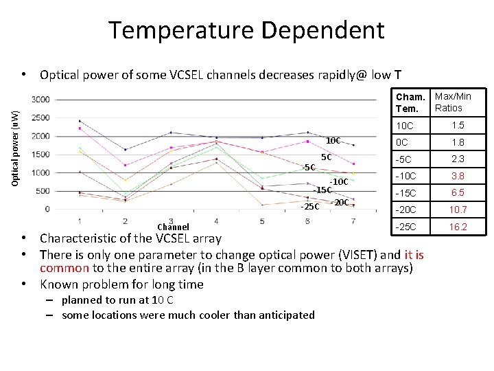
Temperature Dependent • Optical power of some VCSEL channels decreases rapidly@ low T Optical power (u. W) Cham. Tem. Max/Min Ratios 10 C 1. 5 0 C 1. 8 5 C -5 C 2. 3 -10 C -15 C -20 C -10 C 3. 8 -15 C 6. 5 -20 C 10. 7 -25 C 16. 2 10 C -5 C Channel • Characteristic of the VCSEL array • There is only one parameter to change optical power (VISET) and it is common to the entire array (in the B layer common to both arrays) • Known problem for long time – planned to run at 10 C – some locations were much cooler than anticipated

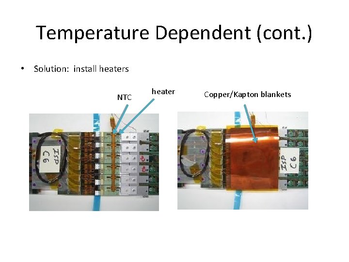
Temperature Dependent (cont. ) • Solution: install heaters NTC heater Copper/Kapton blankets

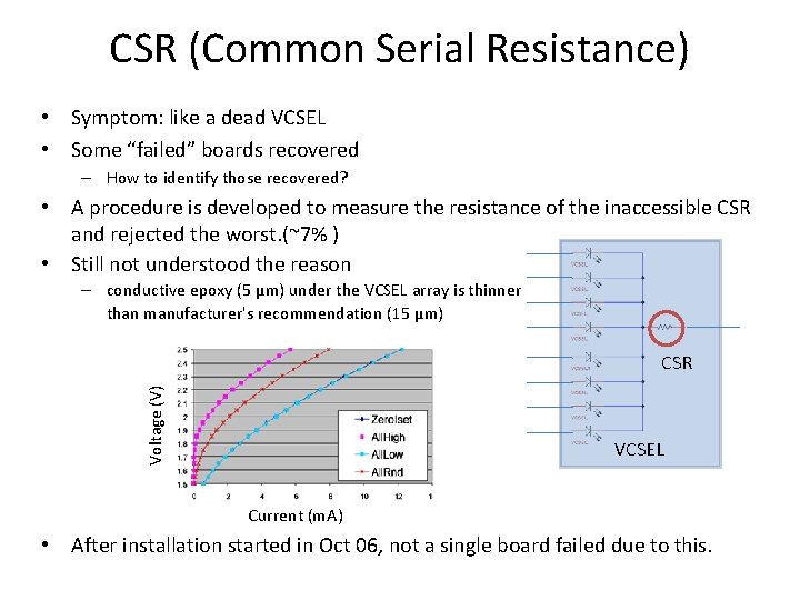
CSR (Common Serial Resistance) • Symptom: like a dead VCSEL • Some “failed” boards recovered – How to identify those recovered? • A procedure is developed to measure the resistance of the inaccessible CSR and rejected the worst. (~7% ) • Still not understood the reason – conductive epoxy (5 μm) under the VCSEL array is thinner than manufacturer's recommendation (15 μm) Voltage (V) CSR VCSEL Current (m. A) • After installation started in Oct 06, not a single board failed due to this.

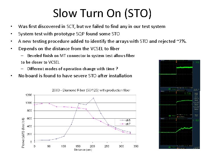
Slow Turn On (STO) • • Was first discovered in SCT, but we failed to find any in our test system System test with prototype SQP found some STO A new testing procedure added to identify the arrays with STO and rejected ~7%. Depends on the distance from the VCSEL to fiber – Beveled finish on MT connector in system test allows fiber to be closer to VCSEL – Different modes of operation change with time ? • No board is found to have severe STO after installation

Current Status • • • Connectivity test – Check the modules can be setup and read out through opto-boards Summary of problems not resolved in the Connectivity test – One dead link due to a failed PIN channel (cold solder? ) rerouted but practically hard to operate. – A short between power and clock in a module – HV wire broken in a cable that is not accessible – Short on one FE chip: module is working with 15 FE chips. Only 4/1744 Modules defective (May be 2 are recoverable)

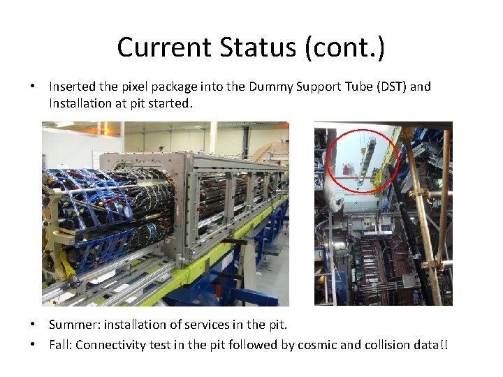
Current Status (cont. ) • Inserted the pixel package into the Dummy Support Tube (DST) and Installation at pit started. • Summer: installation of services in the pit. • Fall: Connectivity test in the pit followed by cosmic and collision data!!