Overview 4 processes Physical Vapor Deposition PVD Chemical
- Slides: 50


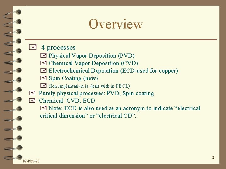
Overview + 4 processes + Physical Vapor Deposition (PVD) + Chemical Vapor Deposition (CVD) + Electrochemical Deposition (ECD-used for copper) + Spin Coating (new) + (Ion implantation is dealt with in FEOL) + Purely physical processes: PVD, Spin coating + Chemical: CVD, ECD + Note: ECD is also used as an acronym to indicate “electrical critical dimension” or “electrical CD”. 02 -Nov-20 2

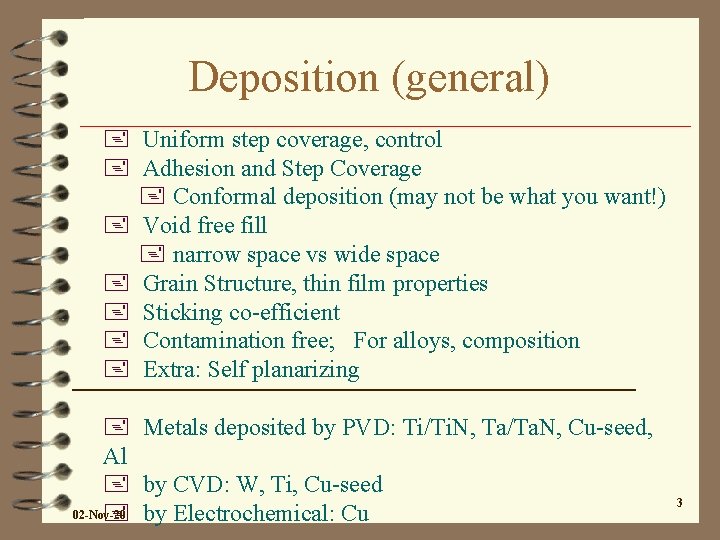
Deposition (general) + Uniform step coverage, control + Adhesion and Step Coverage + Conformal deposition (may not be what you want!) + Void free fill + narrow space vs wide space + Grain Structure, thin film properties + Sticking co-efficient + Contamination free; For alloys, composition + Extra: Self planarizing + Metals deposited by PVD: Ti/Ti. N, Ta/Ta. N, Cu-seed, Al + by CVD: W, Ti, Cu-seed 02 -Nov-20 + by Electrochemical: Cu 3

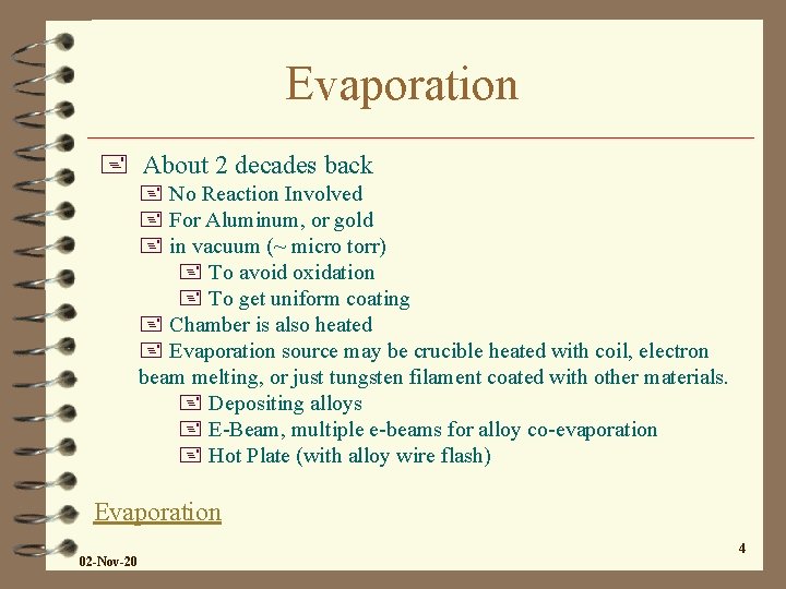
Evaporation + About 2 decades back + No Reaction Involved + For Aluminum, or gold + in vacuum (~ micro torr) + To avoid oxidation + To get uniform coating + Chamber is also heated + Evaporation source may be crucible heated with coil, electron beam melting, or just tungsten filament coated with other materials. + Depositing alloys + E-Beam, multiple e-beams for alloy co-evaporation + Hot Plate (with alloy wire flash) Evaporation 02 -Nov-20 4

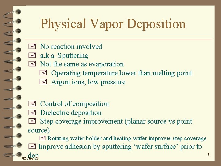
Physical Vapor Deposition + No reaction involved + a. k. a. Sputtering + Not the same as evaporation + Operating temperature lower than melting point + Argon ions, low pressure + Control of composition + Dielectric deposition + Step coverage improvement (planar source vs point source) + Rotating wafer holder and heating wafer improves step coverage + Improve adhesion by sputtering ‘wafer surface’ prior to dep 02 -Nov-20 5

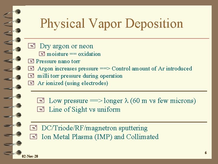
Physical Vapor Deposition + Dry argon or neon + moisture == oxidation + Pressure nano torr + Argon increases pressure ==> Control amount of Ar introduced + milli torr pressure during operation + Ar ionized (using electrodes) + Low pressure ==> longer l (60 m vs few microns) + Line of Sight vs uniform + DC/Triode/RF/magnetron sputtering + Ion Metal Plasma (IMP) and Collimated 02 -Nov-20 6

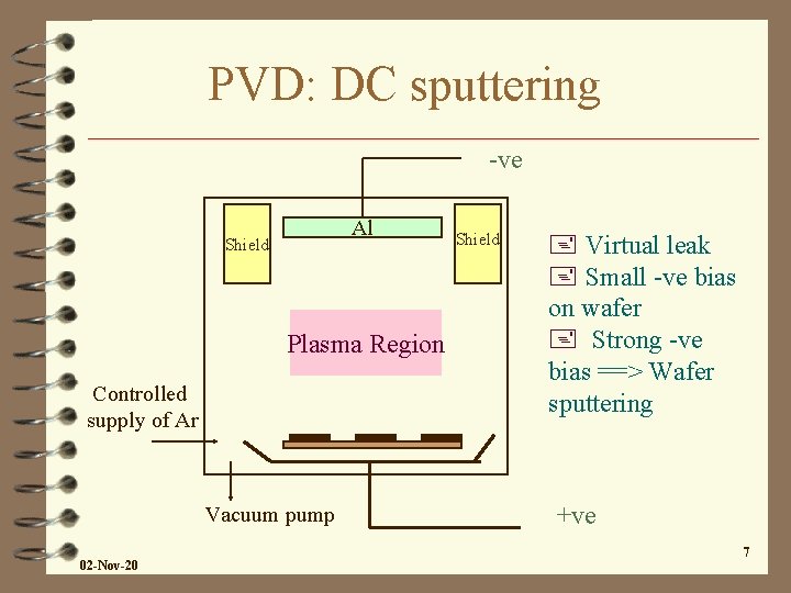
PVD: DC sputtering -ve Al Shield Plasma Region Controlled supply of Ar Vacuum pump 02 -Nov-20 Shield + Virtual leak + Small -ve bias on wafer + Strong -ve bias ==> Wafer sputtering +ve 7

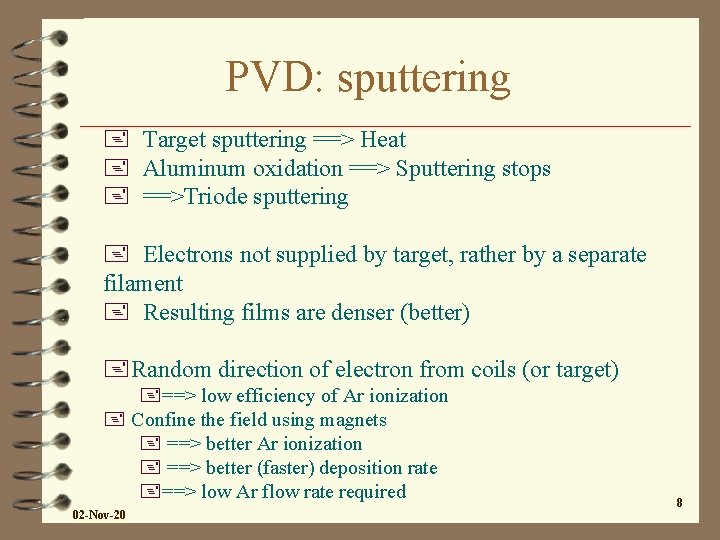
PVD: sputtering + Target sputtering ==> Heat + Aluminum oxidation ==> Sputtering stops + ==>Triode sputtering + Electrons not supplied by target, rather by a separate filament + Resulting films are denser (better) +Random direction of electron from coils (or target) +==> low efficiency of Ar ionization + Confine the field using magnets + ==> better Ar ionization + ==> better (faster) deposition rate +==> low Ar flow rate required 02 -Nov-20 8

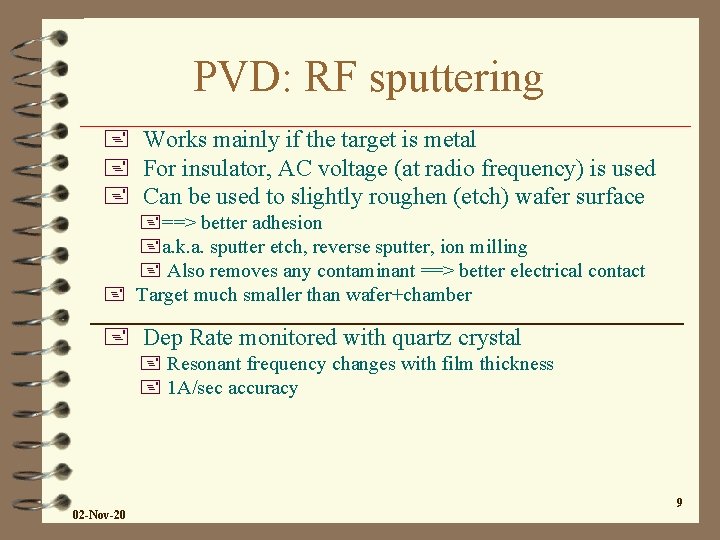
PVD: RF sputtering + Works mainly if the target is metal + For insulator, AC voltage (at radio frequency) is used + Can be used to slightly roughen (etch) wafer surface +==> better adhesion +a. k. a. sputter etch, reverse sputter, ion milling + Also removes any contaminant ==> better electrical contact + Target much smaller than wafer+chamber + Dep Rate monitored with quartz crystal + Resonant frequency changes with film thickness + 1 A/sec accuracy 02 -Nov-20 9

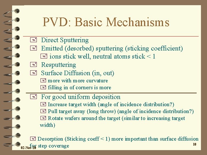
PVD: Basic Mechanisms + Direct Sputtering + Emitted (desorbed) sputtering (sticking coefficient) + ions stick well, neutral atoms stick < 1 + Resputtering + Surface Diffusion (in, out) + more with more curvature + filling in of corners is more + For good uniform deposition + Increase target width (angle of incidence distribution? ) + Pull target away (long throw) (angle of incidence distribution? ) + Rotate wafers around the target (similar to increasing target width) + Desorption (Sticking coeff < 1) more important than surface diffusion 10 for step coverage 02 -Nov-20

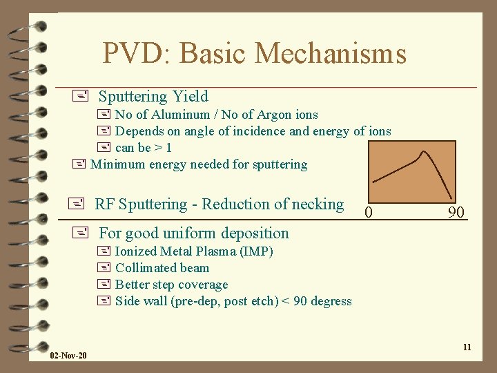
PVD: Basic Mechanisms + Sputtering Yield + No of Aluminum / No of Argon ions + Depends on angle of incidence and energy of ions + can be > 1 + Minimum energy needed for sputtering + RF Sputtering - Reduction of necking 0 90 + For good uniform deposition + Ionized Metal Plasma (IMP) + Collimated beam + Better step coverage + Side wall (pre-dep, post etch) < 90 degress 02 -Nov-20 11

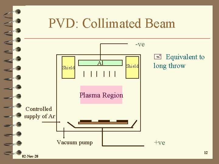
PVD: Collimated Beam -ve Al Shield + Equivalent to long throw Plasma Region Controlled supply of Ar Vacuum pump 02 -Nov-20 +ve 12

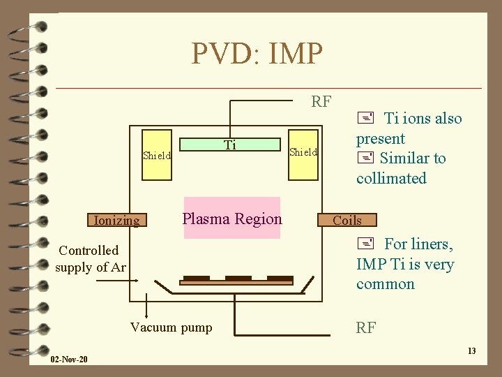
PVD: IMP RF Ti Shield Ionizing Plasma Region Coils + For liners, IMP Ti is very common Controlled supply of Ar Vacuum pump 02 -Nov-20 Shield + Ti ions also present + Similar to collimated RF 13

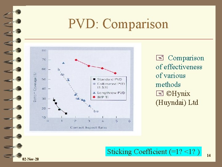
PVD: Comparison + Comparison of effectiveness of various methods + ©Hynix (Huyndai) Ltd Sticking Coefficient (=1? <1? ) 02 -Nov-20 14

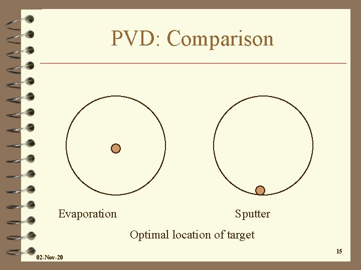
PVD: Comparison Evaporation Sputter Optimal location of target 02 -Nov-20 15

CVD + Reaction occurs on surface + nucleation occurs only on surface + similar to catalysis + Relatively higher pressure compared to PVD + lower mean free path + Anisotropic dep + better step coverage + conformal dep + APCVD, LPCVD, PECVD, HDPCVD, MOCVD + Epitaxy: VPE, LPE, MBE, ALD 02 -Nov-20 16

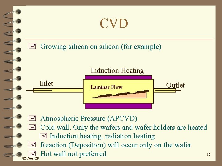
CVD + Growing silicon on silicon (for example) Induction Heating Inlet Laminar Flow Outlet + Atmospheric Pressure (APCVD) + Cold wall. Only the wafers and wafer holders are heated + Induction heating, radiation heating + Reaction (Deposition) will occur only on the wafer 17 + Hot wall not preferred 02 -Nov-20

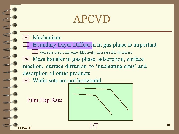
APCVD + Mechanism: + Boundary Layer Diffusion in gas phase is important + decrease press, increase diffusivity, increase BL thickness + Mass transfer in gas phase, adsorption, surface reaction, surface diffusion to ‘nucleating sites’ and desorption of other products + Wafer sets are not horizontal Film Dep Rate 02 -Nov-20 1/T 18

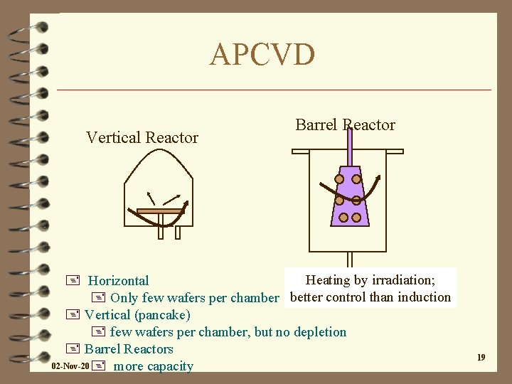
APCVD Vertical Reactor Barrel Reactor Heating by irradiation; + Horizontal + Only few wafers per chamber better control than induction + Vertical (pancake) + few wafers per chamber, but no depletion + Barrel Reactors 02 -Nov-20 + more capacity 19

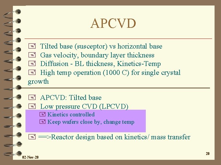
APCVD + Tilted base (susceptor) vs horizontal base + Gas velocity, boundary layer thickness + Diffusion - BL thickness, Kinetics-Temp + High temp operation (1000 C) for single crystal growth + APCVD: Tilted base + Low pressure CVD (LPCVD) + Kinetics controlled + Keep wafers close by, change temp + ==>Reactor design based on kinetics/ mass transfer 02 -Nov-20 20

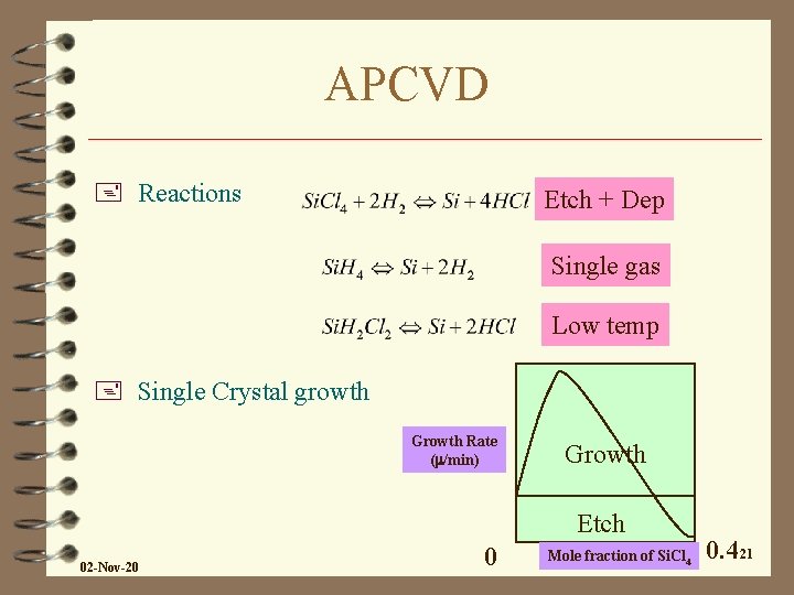
APCVD + Reactions Etch + Dep Single gas Low temp + Single Crystal growth Growth Rate (m/min) Growth Etch 02 -Nov-20 0 Mole fraction of Si. Cl 4 0. 421

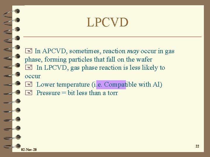
LPCVD + In APCVD, sometimes, reaction may occur in gas phase, forming particles that fall on the wafer + In LPCVD, gas phase reaction is less likely to occur + Lower temperature (i. e. Compatible with Al) + Pressure = bit less than a torr 02 -Nov-20 22

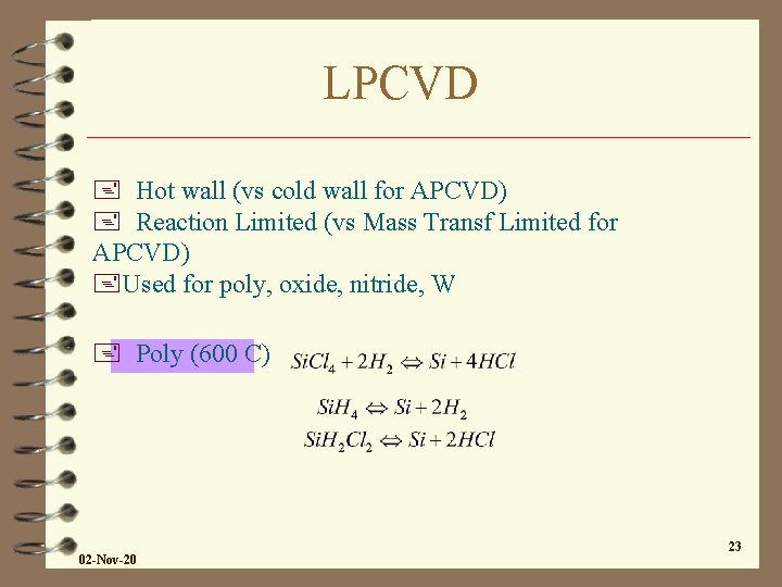
LPCVD + Hot wall (vs cold wall for APCVD) + Reaction Limited (vs Mass Transf Limited for APCVD) +Used for poly, oxide, nitride, W + Poly (600 C) 02 -Nov-20 23

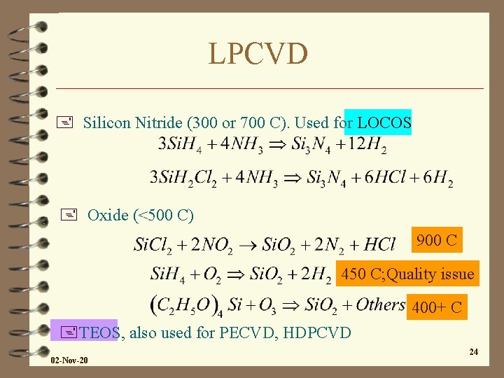
LPCVD + Silicon Nitride (300 or 700 C). Used for LOCOS + Oxide (<500 C) 900 C 450 C; Quality issue 400+ C +TEOS, also used for PECVD, HDPCVD 02 -Nov-20 24

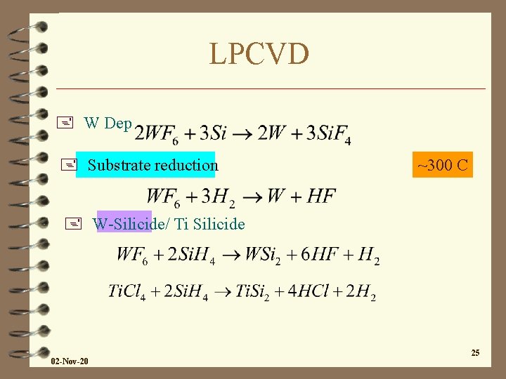
LPCVD + W Dep + Substrate reduction ~300 C + W-Silicide/ Ti Silicide 02 -Nov-20 25

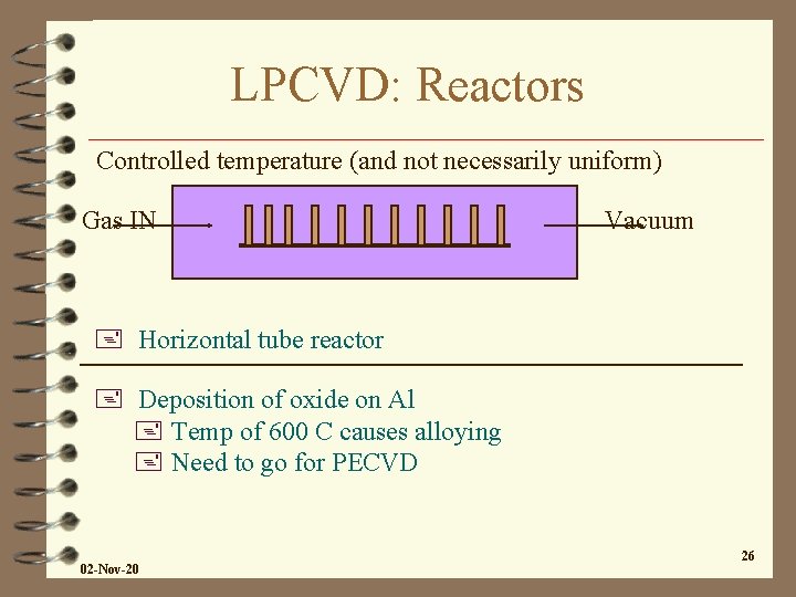
LPCVD: Reactors Controlled temperature (and not necessarily uniform) Gas IN Vacuum + Horizontal tube reactor + Deposition of oxide on Al + Temp of 600 C causes alloying + Need to go for PECVD 02 -Nov-20 26

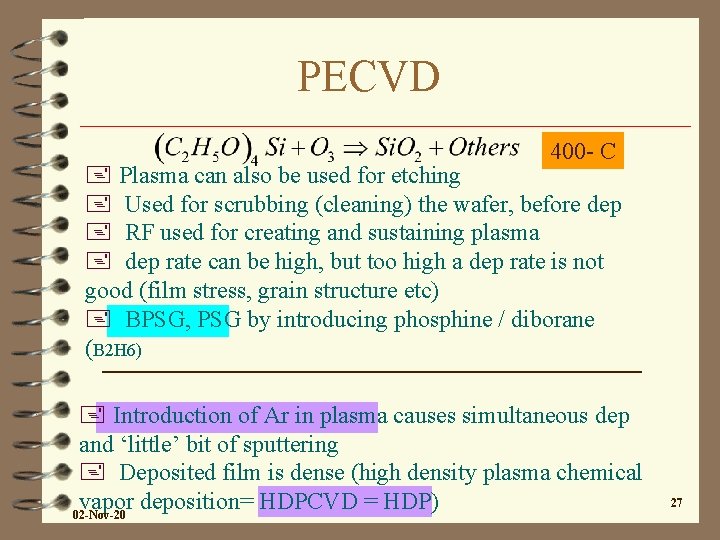
PECVD 400 - C + Plasma can also be used for etching + Used for scrubbing (cleaning) the wafer, before dep + RF used for creating and sustaining plasma + dep rate can be high, but too high a dep rate is not good (film stress, grain structure etc) + BPSG, PSG by introducing phosphine / diborane (B 2 H 6) + Introduction of Ar in plasma causes simultaneous dep and ‘little’ bit of sputtering + Deposited film is dense (high density plasma chemical vapor deposition= HDPCVD = HDP) 02 -Nov-20 27

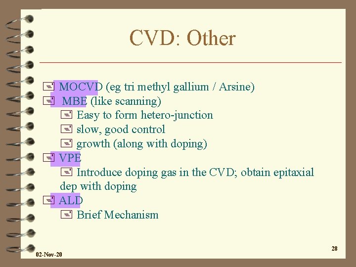
CVD: Other + MOCVD (eg tri methyl gallium / Arsine) + MBE (like scanning) + Easy to form hetero-junction + slow, good control + growth (along with doping) + VPE + Introduce doping gas in the CVD; obtain epitaxial dep with doping + ALD + Brief Mechanism 02 -Nov-20 28

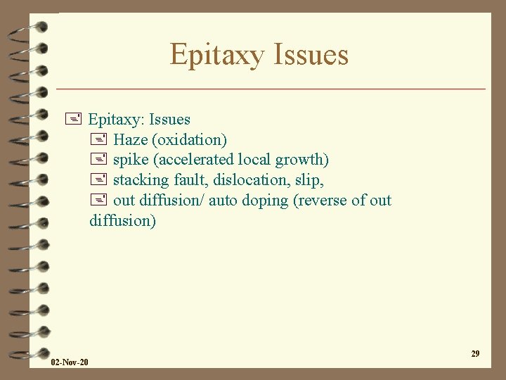
Epitaxy Issues + Epitaxy: Issues + Haze (oxidation) + spike (accelerated local growth) + stacking fault, dislocation, slip, + out diffusion/ auto doping (reverse of out diffusion) 02 -Nov-20 29

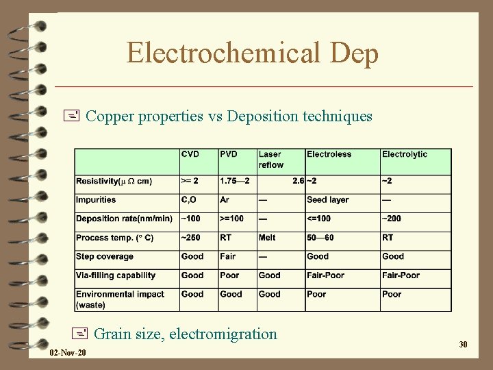
Electrochemical Dep + Copper properties vs Deposition techniques + Grain size, electromigration 02 -Nov-20 30

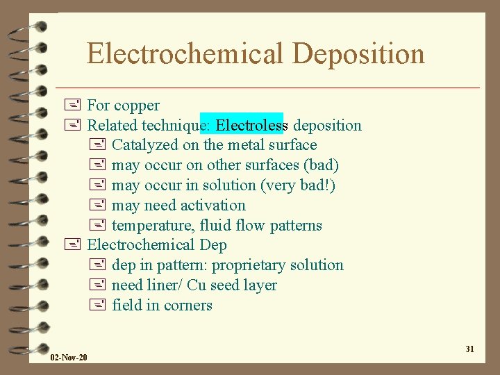
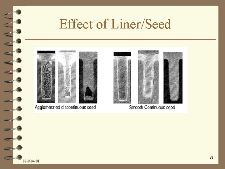
Electrochemical Deposition + For copper + Related technique: Electroless deposition + Catalyzed on the metal surface + may occur on other surfaces (bad) + may occur in solution (very bad!) + may need activation + temperature, fluid flow patterns + Electrochemical Dep + dep in pattern: proprietary solution + need liner/ Cu seed layer + field in corners 02 -Nov-20 31

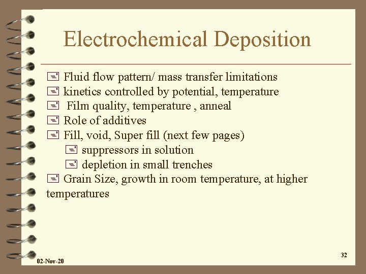
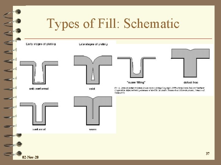
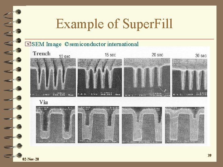
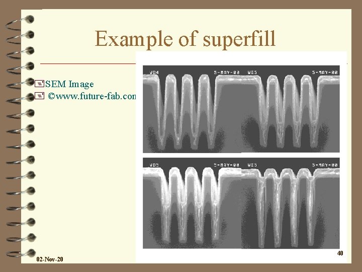
Electrochemical Deposition + Fluid flow pattern/ mass transfer limitations + kinetics controlled by potential, temperature + Film quality, temperature , anneal + Role of additives + Fill, void, Super fill (next few pages) + suppressors in solution + depletion in small trenches + Grain Size, growth in room temperature, at higher temperatures 02 -Nov-20 32

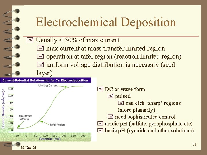
Electrochemical Deposition + Usually < 50% of max current + max current at mass transfer limited region + operation at tafel region (reaction limited region) + uniform voltage distribution is necessary (seed layer) + convection is key + DC or wave form + pulsed + can etch ‘sharp’ regions (more planarity) + need sophisticated control + acidic p. H (sulfate, pyrophosphate etc) + basic p. H (cyanide and other solutions) 02 -Nov-20 33

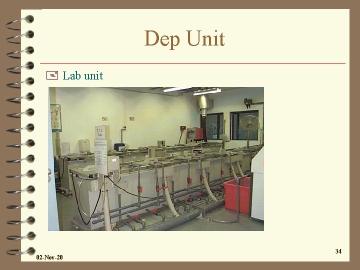
Dep Unit + Lab unit 02 -Nov-20 34

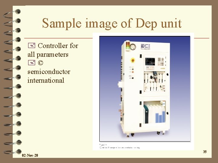
Sample image of Dep unit + Controller for all parameters +© semiconductor international 02 -Nov-20 35

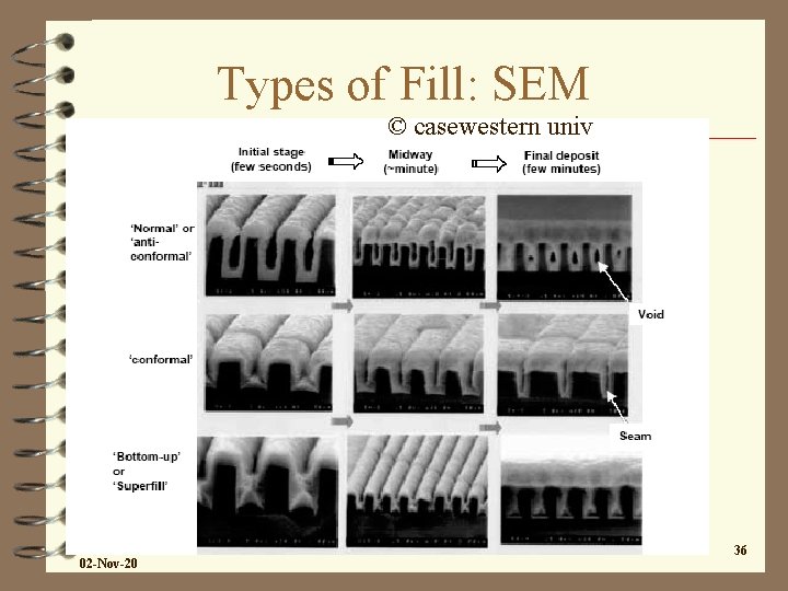
Types of Fill: SEM © casewestern univ 02 -Nov-20 36

Types of Fill: Schematic 02 -Nov-20 37

Effect of Liner/Seed 02 -Nov-20 38

Example of Super. Fill +SEM Image ©semiconductor international 02 -Nov-20 39

Example of superfill +SEM Image + ©www. future-fab. com 02 -Nov-20 40

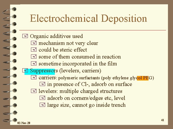
Electrochemical Deposition + Organic additives used + mechanism not very clear + could be steric effect + some of them consumed in reaction + sometime incorporated in the film + Suppressors (levelers, carriers) + carriers: polymeric surfactants (poly ethylene glycol PEG) + in presence of Cl-, adsorb on surface + levelers: multiple charged structures + adsorb on corners/edges etc, level + large size, cannot go inside trench 02 -Nov-20 41

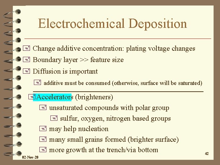
Electrochemical Deposition + Change additive concentration: plating voltage changes + Boundary layer >> feature size + Diffusion is important + additive must be consumed (otherwise, surface will be saturated) +Accelerators (brighteners) + unsaturated compounds with polar group + sulfur, oxygen, nitrogen based groups + may help nucleation + many small grains formed (brighter surface) + more growth at the trench/via bottom 02 -Nov-20 42

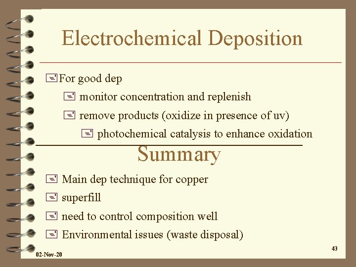
Electrochemical Deposition +For good dep + monitor concentration and replenish + remove products (oxidize in presence of uv) + photochemical catalysis to enhance oxidation Summary + Main dep technique for copper + superfill + need to control composition well + Environmental issues (waste disposal) 02 -Nov-20 43

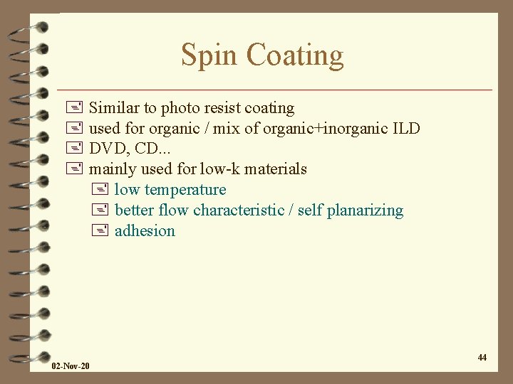
Spin Coating + Similar to photo resist coating + used for organic / mix of organic+inorganic ILD + DVD, CD. . . + mainly used for low-k materials + low temperature + better flow characteristic / self planarizing + adhesion 02 -Nov-20 44

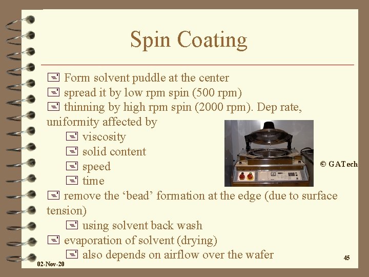
Spin Coating + Form solvent puddle at the center + spread it by low rpm spin (500 rpm) + thinning by high rpm spin (2000 rpm). Dep rate, uniformity affected by + viscosity + solid content © GATech + speed + time + remove the ‘bead’ formation at the edge (due to surface tension) + using solvent back wash + evaporation of solvent (drying) + also depends on airflow over the wafer 45 02 -Nov-20

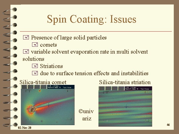
Spin Coating: Issues + Presence of large solid particles + comets + variable solvent evaporation rate in multi solvent solutions + Striations + due to surface tension effects and instabilities Silica-titania comet Silica-titania striation ©univ ariz 02 -Nov-20 46

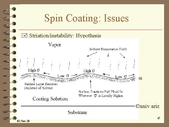
Spin Coating: Issues + Striation/instability: Hypothesis Silica-titania striation ©univ ariz 02 -Nov-20 47

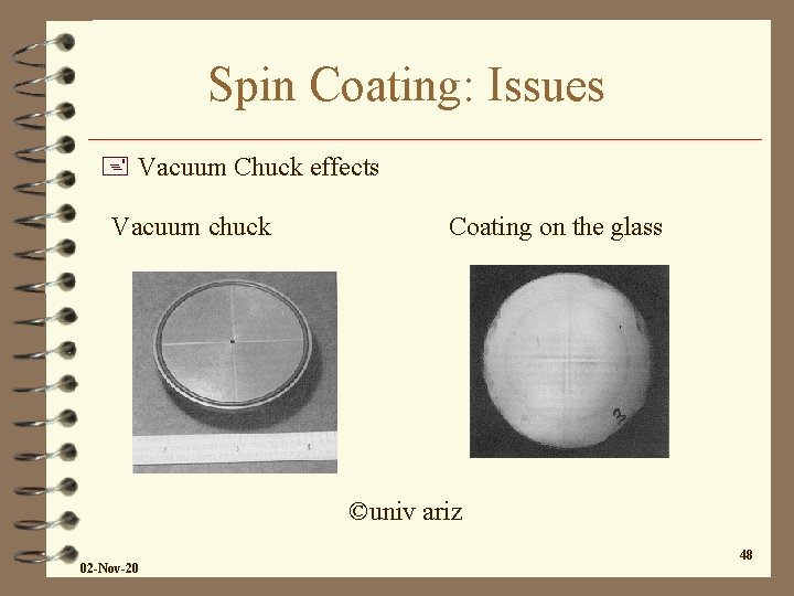
Spin Coating: Issues + Vacuum Chuck effects Vacuum chuck Coating on the glass ©univ ariz 02 -Nov-20 48

Spin Coating: Issues + Note: outside the O-ring variations + Near the ‘grooves’ clear variation + Hypothesis: + heat from chuck compensates for cooling by evaporation + when there is no contact, cooling is not ‘prevented’ + ==> lower evaporation when there is no contact + more pronounced in glass vs silicon (better heat conductor) 02 -Nov-20 49

Spin Coating: Summary + In R&D + Similar to photo resist coating + Goal is to use it for low-k dielectrics (insulators) + Issues yet to be resolved + Most of the issues in low-k are not with spin coating. They are with subsequent processes / integration 02 -Nov-20 50