Overview 1 Motivation Kevin 2 Thermal issues Kevin




- Slides: 45

Overview 1. Motivation (Kevin) 2. Thermal issues (Kevin) 3. Power modeling (David) 4. Thermal management (David) 5. Optimal DTM (Lev) 6. Clustering (Antonio) 7. Power distribution (David) 8. What current chips do (Lev) 9. Hot. Spot and sensors (Kevin)

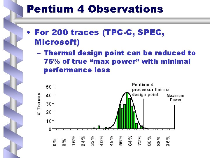
Pentium 4 Observations • For 200 traces (TPC-C, SPEC, Microsoft) – Thermal design point can be reduced to 75% of true “max power” with minimal performance loss

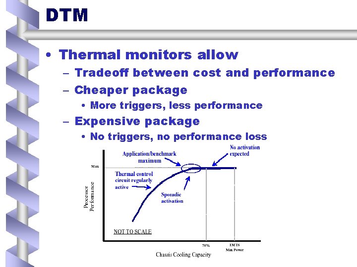
DTM • Thermal monitors allow – Tradeoff between cost and performance – Cheaper package • More triggers, less performance – Expensive package • No triggers, no performance loss

Architecture-level Thermal Management • Dynamically adjust execution to control temperature • Avoid catastrophic failure (heat sink, fan) • Permit use of less expensive package – Design for less than the worst case – Package costs ~$1/W above ~40 W – Heat sinks, heat pipes, thinned wafers, fans • Fans reduce battery life – Peak power as high as 150 W now and > 200 W in 1 -2 generations – Temperatures over 100°C • More fundamentally -- there is a need for architecture-level thermal modeling – What’s actually going on in there?

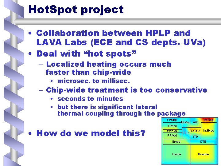
Hot. Spot project • Collaboration between HPLP and LAVA Labs (ECE and CS depts. UVa) • Deal with “hot spots” – Localized heating occurs much faster than chip-wide • microsec. to millisec. – Chip-wide treatment is too conservative • seconds to minutes • but there is significant lateral thermal coupling through the package • How do we model this?

Thermal modeling • Want a fine-grained, dynamic model of temperature – At a granularity architects can reason about – That accounts for adjacency and package – That does not require detailed designs – That is fast enough for practical use • Hot. Spot - a compact model based on thermal R, C – Parameterized to automatically derive a model based on various • • Architectures Power models Floorplans Thermal Packages

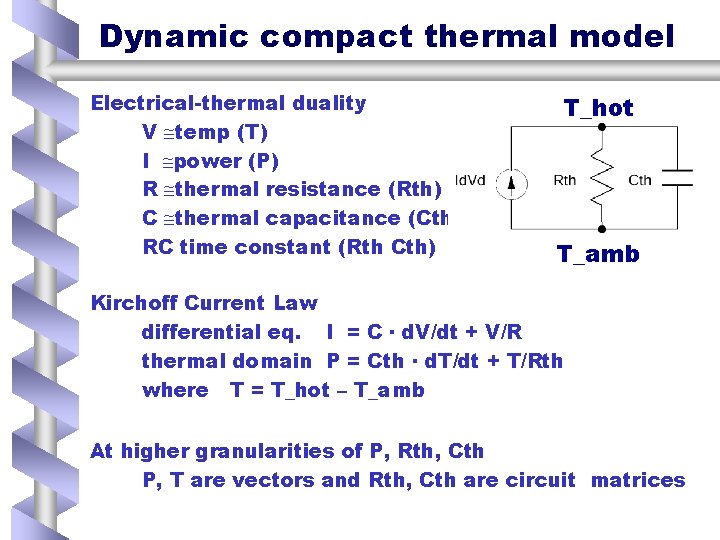
Dynamic compact thermal model Electrical-thermal duality V temp (T) I power (P) R thermal resistance (Rth) C thermal capacitance (Cth) RC time constant (Rth Cth) T_hot T_amb Kirchoff Current Law differential eq. I = C · d. V/dt + V/R thermal domain P = Cth · d. T/dt + T/Rth where T = T_hot – T_amb At higher granularities of P, Rth, Cth P, T are vectors and Rth, Cth are circuit matrices

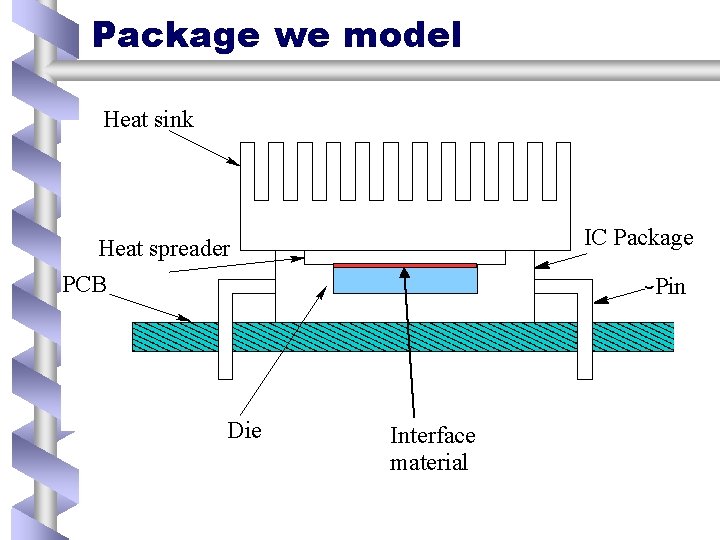
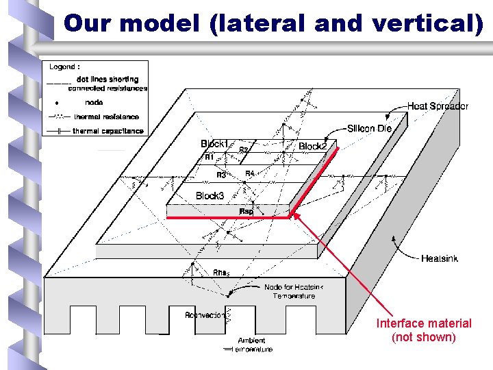
Package we model Heat sink IC Package Heat spreader PCB Die Pin Interface material

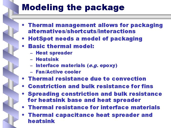
Modeling the package • Thermal management allows for packaging alternatives/shortcuts/interactions • Hot. Spot needs a model of packaging • Basic thermal model: – – Heat spreader Heatsink Interface materials (e. g. epoxy) Fan/Active cooler • Thermal resistance due to convection • Constriction and bulk resistance for fins • Spreading constriction and bulk resistance for heatsink base and heat spreader • Thermal resistance for interface materials • Thermal capacitance heat spreader and heatsink

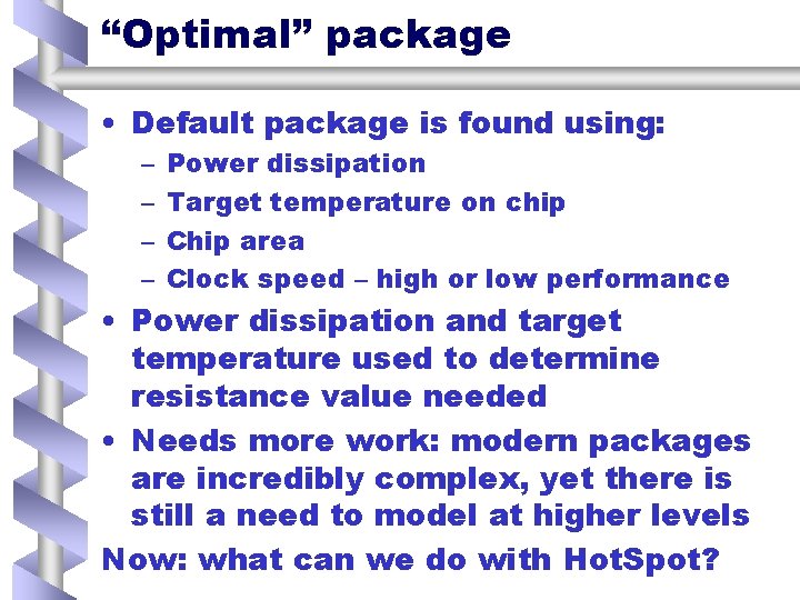
“Optimal” package • Default package is found using: – – Power dissipation Target temperature on chip Chip area Clock speed – high or low performance • Power dissipation and target temperature used to determine resistance value needed • Needs more work: modern packages are incredibly complex, yet there is still a need to model at higher levels Now: what can we do with Hot. Spot?

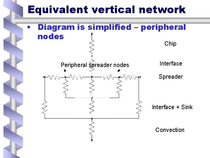
Equivalent vertical network • Diagram is simplified – peripheral nodes Chip Peripheral spreader nodes Interface Spreader Interface + Sink Convection

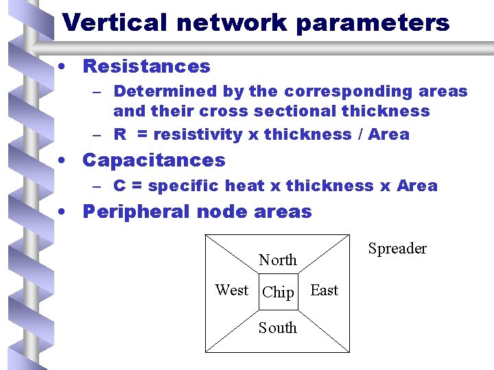
Vertical network parameters • Resistances – Determined by the corresponding areas and their cross sectional thickness – R = resistivity x thickness / Area • Capacitances – C = specific heat x thickness x Area • Peripheral node areas North West Chip East South Spreader

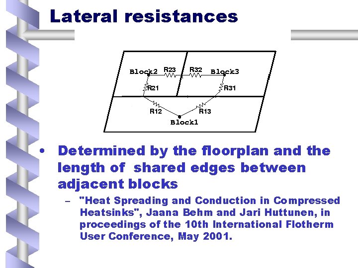
Lateral resistances • Determined by the floorplan and the length of shared edges between adjacent blocks – "Heat Spreading and Conduction in Compressed Heatsinks", Jaana Behm and Jari Huttunen, in proceedings of the 10 th International Flotherm User Conference, May 2001.

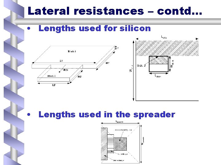
Lateral resistances – contd. . . • Lengths used for silicon • Lengths used in the spreader

Our model (lateral and vertical) Interface material (not shown)

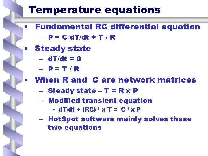
Temperature equations • Fundamental RC differential equation – P = C d. T/dt + T / R • Steady state – d. T/dt = 0 – P=T/R • When R and C are network matrices – Steady state – T = R x P – Modified transient equation • d. T/dt + (RC)-1 x T = C-1 x P – Hot. Spot software mainly solves these two equations

Hot. Spot • Time evolution of temperature is driven by unit activities and power dissipations averaged over 10 K cycles – Power dissipations can come from any power simulator, act as “current sources” in RC circuit ('P' vector in the equations) – Simulation overhead in Wattch/Simple. Scalar: < 1% • Requires models of – Floorplan: important for adjacency – Package: important for spreading and time constants – R and C matrices are derived from the above

Implementation • • Primarily a circuit solver Steady state solution – Mainly matrix inversion – done in two steps • Decomposition of the matrix into lower and upper triangular matrices • Successive backward substitution of solved variables – Implements the pseudocode from CLR • Transient solution – Inputs – current temperature and power – Output – temperature for the next interval – Computed using a fourth order Runge-Kutta (RK 4) method

Transient solution • Solves differential equations of the form d. T + AT = B where A and B are constants – In Hot. Spot, A is constant (RC) but B depends on the power dissipation – Solution – assume constant average power dissipation within an interval (10 K cycles) and call RK 4 at the end of each interval • • In RK 4, current temperature (at t) is advanced in very small steps (t+h, t+2 h. . . ) till the next interval (10 K cycles) RK – `4` because error term is 4 th order i. e. , O(h^4)

Transient solution contd. . . • 4 th order error has to be within the required precision • The step size (h) has to be small enough even for the maximum slope of the temperature evolution curve • Transient solution for the differential equation is of the form Ae-Bt with A and B are dependent on the RC network • Thus, the maximum value of the slope (Ax. B) and the step size are computed accordingly

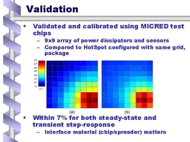
Validation • Validated and calibrated using MICRED test chips – 9 x 9 array of power dissipators and sensors – Compared to Hot. Spot configured with same grid, package • Within 7% for both steady-state and transient step-response – Interface material (chip/spreader) matters

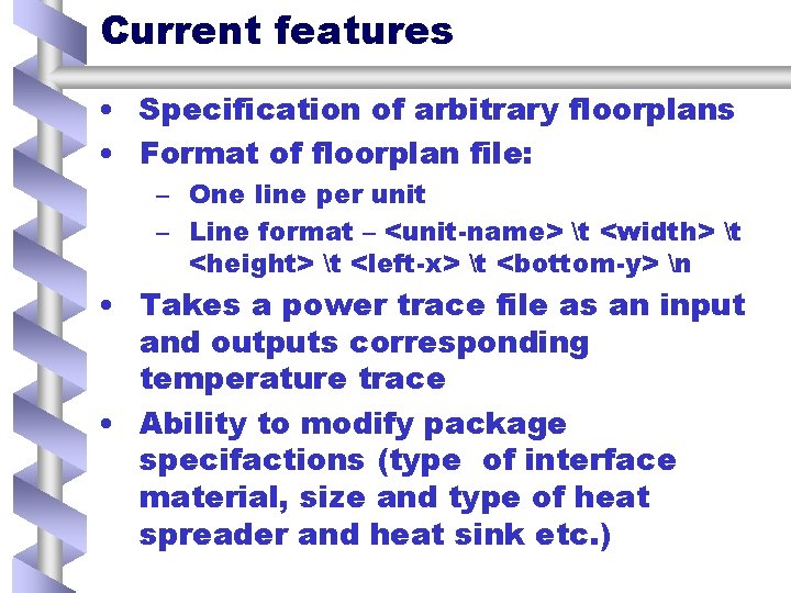
Current features • Specification of arbitrary floorplans • Format of floorplan file: – One line per unit – Line format – <unit-name> t <width> t <height> t <left-x> t <bottom-y> n • Takes a power trace file as an input and outputs corresponding temperature trace • Ability to modify package specifactions (type of interface material, size and type of heat spreader and heat sink etc. )

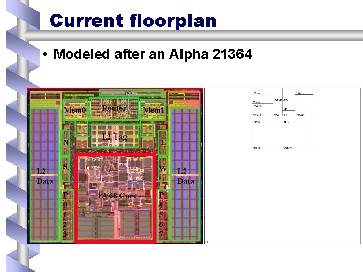
Current floorplan • Modeled after an Alpha 21364

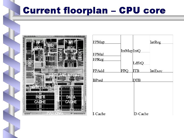
Current floorplan – CPU core

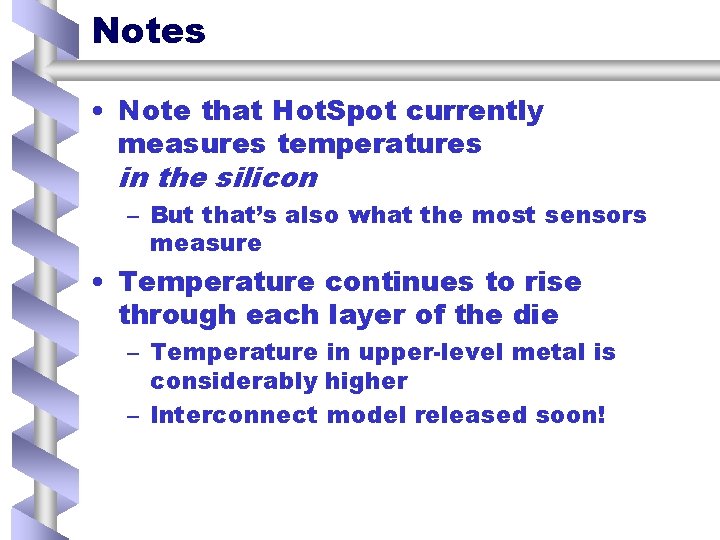
Notes • Note that Hot. Spot currently measures temperatures in the silicon – But that’s also what the most sensors measure • Temperature continues to rise through each layer of the die – Temperature in upper-level metal is considerably higher – Interconnect model released soon!

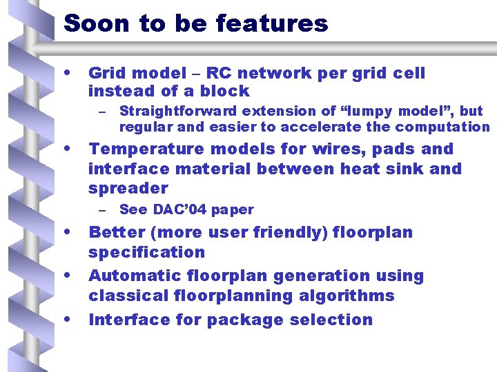
Soon to be features • Grid model – RC network per grid cell instead of a block – Straightforward extension of “lumpy model”, but regular and easier to accelerate the computation • Temperature models for wires, pads and interface material between heat sink and spreader – See DAC’ 04 paper • • • Better (more user friendly) floorplan specification Automatic floorplan generation using classical floorplanning algorithms Interface for package selection

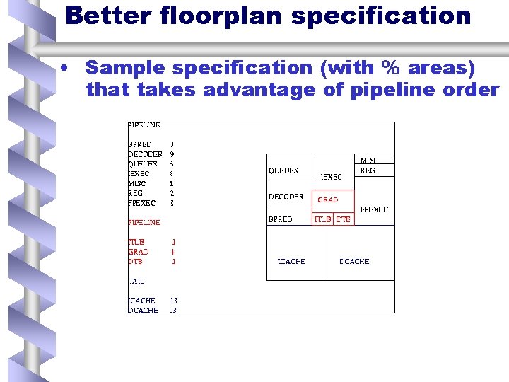
Better floorplan specification • Floorplan of current microprocessors has a structural similarity • Floorplans similar to MIPS R 10 K, Pentium and the Alpha 21264 • Pipeline order corresponds to floorplan adjacency

Better floorplan specification • Sample specification (with % areas) that takes advantage of pipeline order

Automatic floorplan for architects • Why develop an architectural floorplanning tool? – Thermal modeling requires adjacency information. – Wire delays make performance depend on the floorplan. • Goal – Derive a realistic floorplan using only microarchitectural information – Trade off thermal efficiency against latency – Simulated annealing based floorplan optimization for thermal, delay and combined metrics • Current work. Results will be available soon

Hot. Spot Summary • Hot. Spot is a simple, accurate and fast architecture level thermal model for microprocessors • Over 150 downloads since June’ 03 • Ongoing active development – architecture level floorplanning will be available soon • Download site – http: //lava. cs. virginia. edu/Hot. Spot • Mailing list – www. cs. virginia. edu/mailman/listinfo/hotspot

Sensors Caveat emptor: We are not well-versed on sensor design; the following is a digest of information we have been able to collect from industry sources and the research literature.

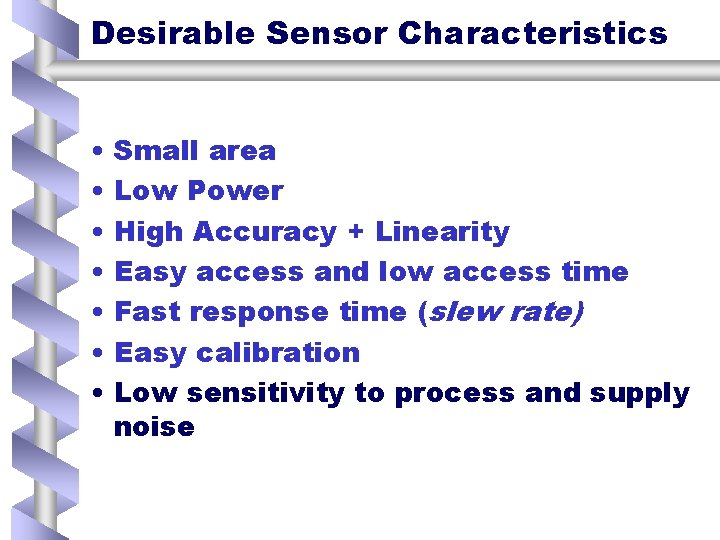
Desirable Sensor Characteristics • Small area • Low Power • High Accuracy + Linearity • Easy access and low access time • Fast response time (slew rate) • Easy calibration • Low sensitivity to process and supply noise

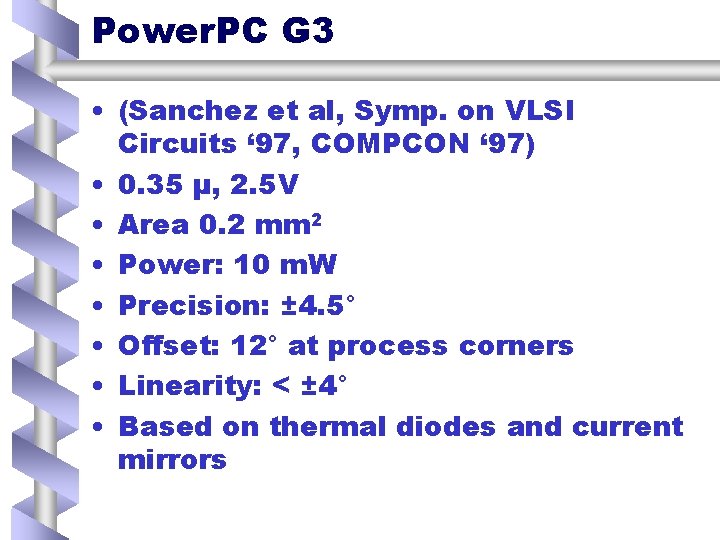
Power. PC G 3 • (Sanchez et al, Symp. on VLSI Circuits ‘ 97, COMPCON ‘ 97) • 0. 35 μ, 2. 5 V • Area 0. 2 mm 2 • Power: 10 m. W • Precision: ± 4. 5° • Offset: 12° at process corners • Linearity: < ± 4° • Based on thermal diodes and current mirrors

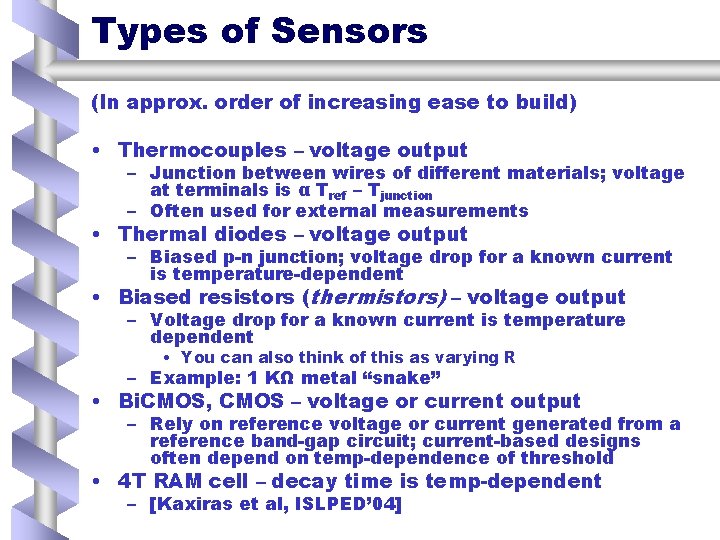
Types of Sensors (In approx. order of increasing ease to build) • Thermocouples – voltage output – Junction between wires of different materials; voltage at terminals is α Tref – Tjunction – Often used for external measurements • Thermal diodes – voltage output – Biased p-n junction; voltage drop for a known current is temperature-dependent • Biased resistors (thermistors) – voltage output – Voltage drop for a known current is temperature dependent • You can also think of this as varying R – Example: 1 KΩ metal “snake” • Bi. CMOS, CMOS – voltage or current output – Rely on reference voltage or current generated from a reference band-gap circuit; current-based designs often depend on temp-dependence of threshold • 4 T RAM cell – decay time is temp-dependent – [Kaxiras et al, ISLPED’ 04]

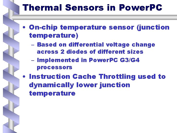
Thermal Sensors in Power. PC • On-chip temperature sensor (junction temperature) – Based on differential voltage change across 2 diodes of different sizes – Implemented in Power. PC G 3/G 4 processors • Instruction Cache Throttling used to dynamically lower junction temperature

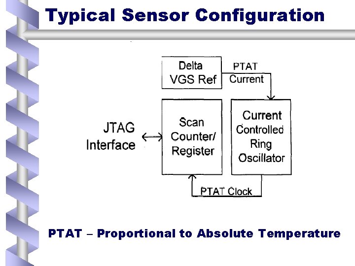
Typical Sensor Configuration PTAT – Proportional to Absolute Temperature

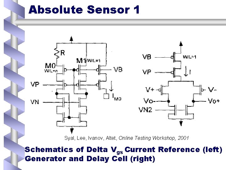
Absolute Sensor 1 Syal, Lee, Ivanov, Altet, Online Testing Workshop, 2001 Schematics of Delta Vgs Current Reference (left) Generator and Delay Cell (right)

Sensors: Problem Issues • Poor control of CMOS transistor parameters • Noisy environment – Cross talk – Ground noise – Power supply noise • These can be reduced by making the sensor larger – This increases power dissipation – But we may want many sensors

“Reasonable” Values • Based on conversations with engineers at Sun, Intel, and HP (Alpha) • Linearity: not a problem for range of temperatures of interest • Slew rate: < 1 μs – This is the time it takes for the physical sensing process (e. g. , current) to reach equilibrium • Sensor bandwidth: << 1 MHz, probably 100 -200 k. Hz – This is the sampling rate; 100 k. Hz = 10 μs – Limited by slew rate but also A/D • Consider digitization using a counter

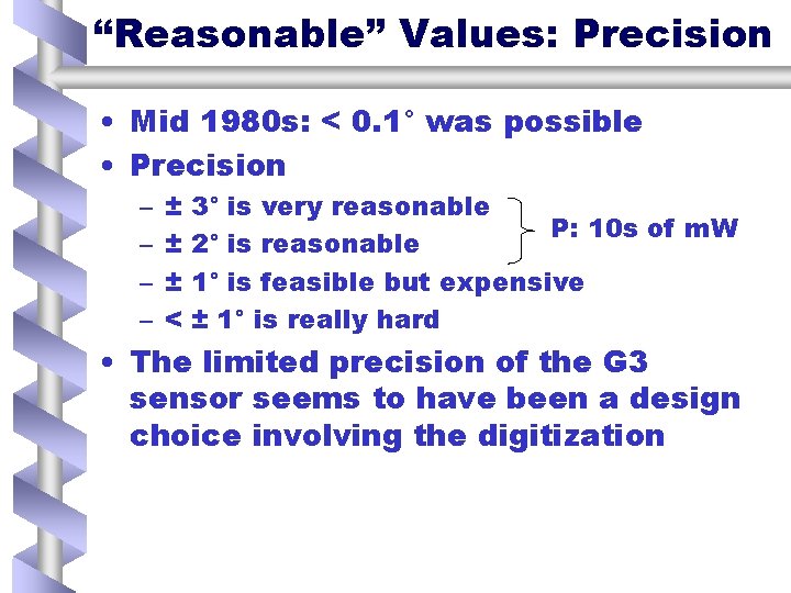
“Reasonable” Values: Precision • Mid 1980 s: < 0. 1° was possible • Precision – – ± ± ± < 3° is very reasonable P: 10 s of m. W 2° is reasonable 1° is feasible but expensive ± 1° is really hard • The limited precision of the G 3 sensor seems to have been a design choice involving the digitization

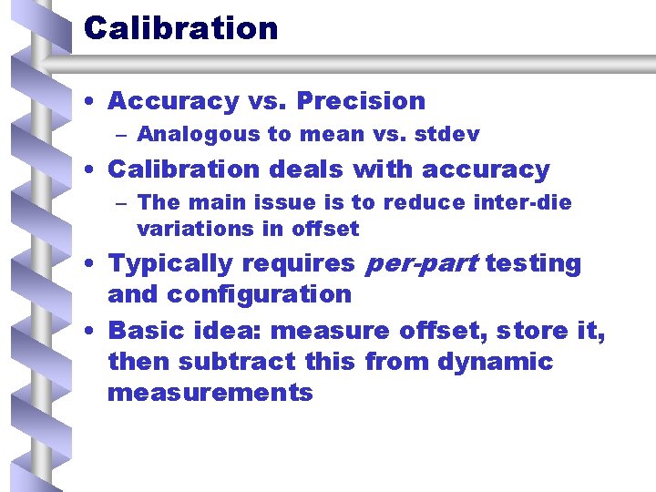
Calibration • Accuracy vs. Precision – Analogous to mean vs. stdev • Calibration deals with accuracy – The main issue is to reduce inter-die variations in offset • Typically requires per-part testing and configuration • Basic idea: measure offset, store it, then subtract this from dynamic measurements

Dynamic Offset Cancelation • Rich area of research • Build circuit to continuously, dynamically detect offset and cancel it • Typically uses an op-amp • Has the advantage that it adapts to changing offsets • Has the disadvantage of more complex circuitry

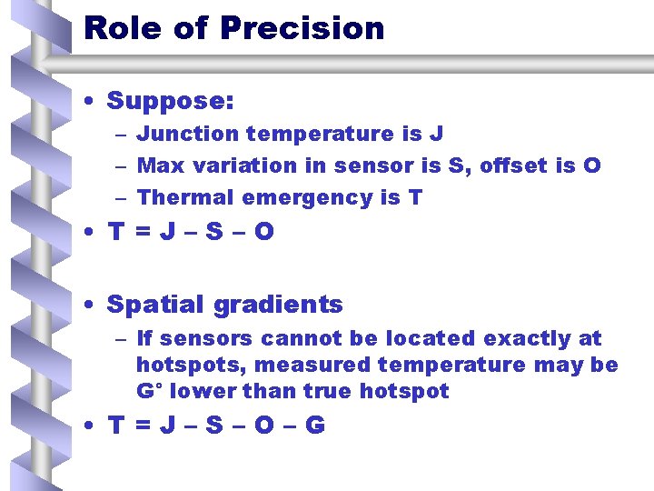
Role of Precision • Suppose: – Junction temperature is J – Max variation in sensor is S, offset is O – Thermal emergency is T • T=J–S–O • Spatial gradients – If sensors cannot be located exactly at hotspots, measured temperature may be G° lower than true hotspot • T=J–S–O–G

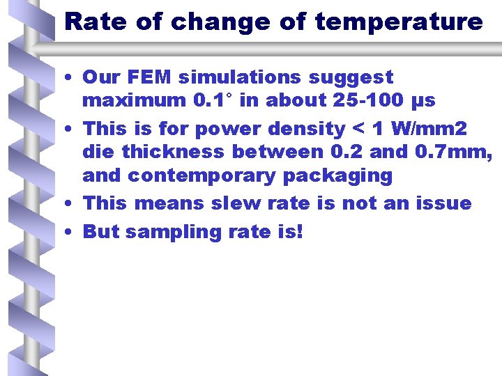
Rate of change of temperature • Our FEM simulations suggest maximum 0. 1° in about 25 -100 μs • This is for power density < 1 W/mm 2 die thickness between 0. 2 and 0. 7 mm, and contemporary packaging • This means slew rate is not an issue • But sampling rate is!

Sensors Summary • Sensor precision cannot be ignored – Reducing operating threshold by 1 -2 degrees will affect performance • Precision of 1° is conceivable but expensive – Maybe reasonable for a single sensor or a few • Precision of 2 -3° is reasonable even for a moderate number of sensors • Power and area are probably negligible from the architecture standpoint • Sampling period <= 10 -20 μs