OUTLINE n Introduction n Basics of the Verilog
OUTLINE n Introduction n Basics of the Verilog Language n Gate-level modeling n Data-flow modeling n Behavioral modeling n Task and function
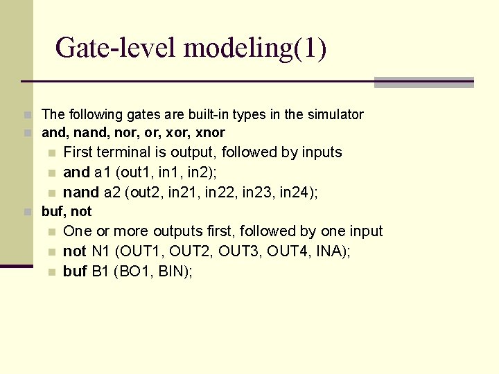
Gate-level modeling(1) n The following gates are built-in types in the simulator n and, nor, xor, xnor n n n First terminal is output, followed by inputs and a 1 (out 1, in 2); nand a 2 (out 2, in 21, in 22, in 23, in 24); n buf, not n n n One or more outputs first, followed by one input not N 1 (OUT 1, OUT 2, OUT 3, OUT 4, INA); buf B 1 (BO 1, BIN);
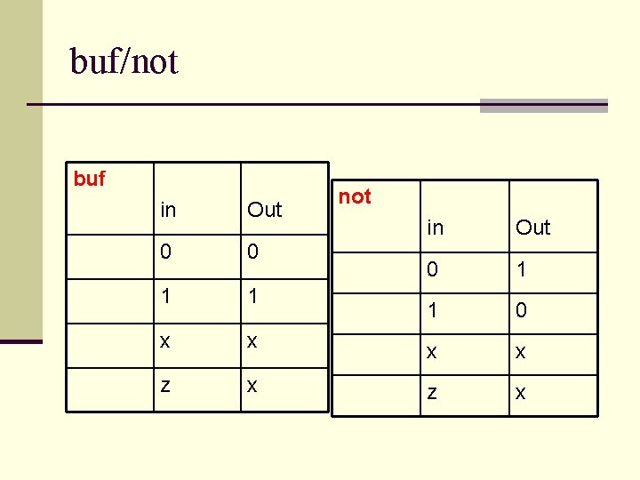
buf/not buf in Out 0 0 1 1 x x z x not in Out 0 1 1 0 x x z x
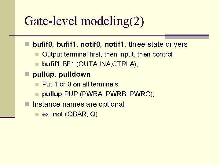
Gate-level modeling(2) n bufif 0, bufif 1, notif 0, notif 1: three-state drivers n Output terminal first, then input, then control n bufif 1 BF 1 (OUTA, INA, CTRLA); n pullup, pulldown n Put 1 or 0 on all terminals n pullup PUP (PWRA, PWRB, PWRC); n Instance names are optional n ex: not (QBAR, Q)
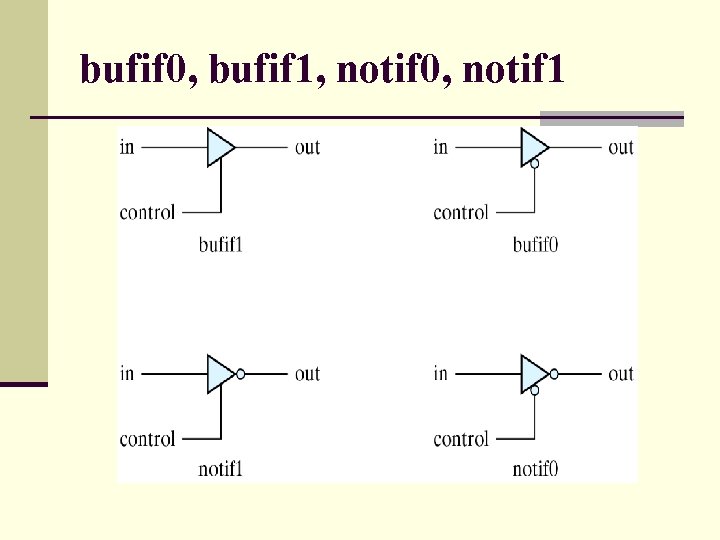
bufif 0, bufif 1, notif 0, notif 1
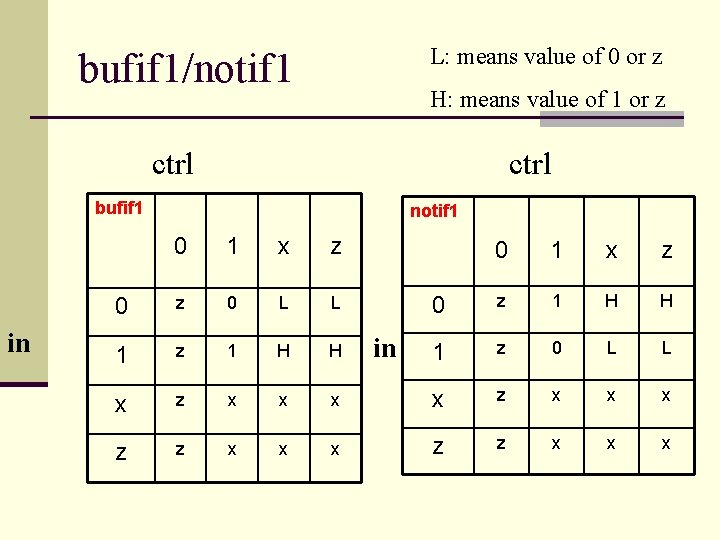
L: means value of 0 or z bufif 1/notif 1 H: means value of 1 or z ctrl bufif 1 in notif 1 0 1 x z 0 L L 1 z 1 H H x z x x z z x x 0 1 x z 0 z 1 H H 1 z 0 L L x x z z x x x in
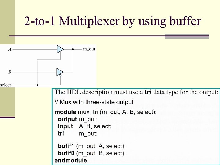
2 -to-1 Multiplexer by using buffer
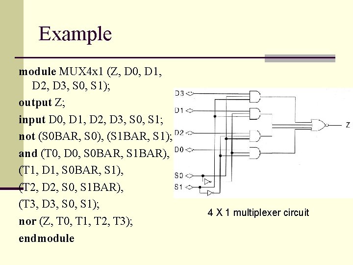
Example module MUX 4 x 1 (Z, D 0, D 1, D 2, D 3, S 0, S 1); output Z; input D 0, D 1, D 2, D 3, S 0, S 1; not (S 0 BAR, S 0), (S 1 BAR, S 1); and (T 0, D 0, S 0 BAR, S 1 BAR), (T 1, D 1, S 0 BAR, S 1), (T 2, D 2, S 0, S 1 BAR), (T 3, D 3, S 0, S 1); nor (Z, T 0, T 1, T 2, T 3); endmodule 4 X 1 multiplexer circuit
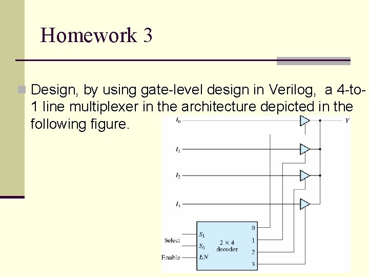
Homework 3 n Design, by using gate-level design in Verilog, a 4 -to- 1 line multiplexer in the architecture depicted in the following figure.
OUTLINE n Introduction n Basics of the Verilog Language n Gate-level modeling n Data-flow modeling n Behavioral modeling n Task and function
Data-flow modeling(1) n Higher level than gate level n Design circuit in terms of the data flow between register n Can be viewed as part of RTL n RTL=behavior modeling + data-flow modeling n Assign a value to a net using continuous assignment
![Example wire [3: 0] Z, PRESET, CLEAR; assign Z = PRESET & CLEAR; wire Example wire [3: 0] Z, PRESET, CLEAR; assign Z = PRESET & CLEAR; wire](http://slidetodoc.com/presentation_image_h2/55036839ea001bacb60a304ce45307f9/image-12.jpg)
Example wire [3: 0] Z, PRESET, CLEAR; assign Z = PRESET & CLEAR; wire COUT, CIN; wire [3: 0] SUM, A, B; assign {COUT, SUM} = A + B + CIN;
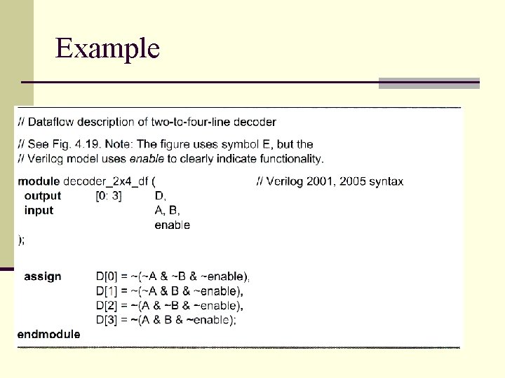
Example
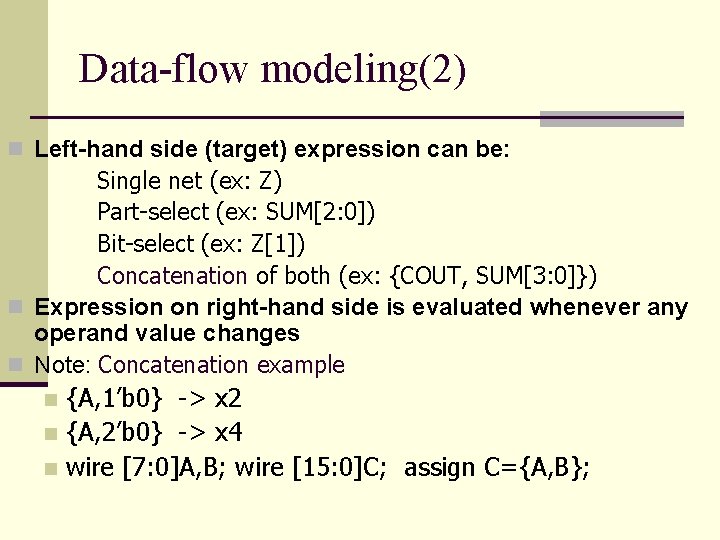
Data-flow modeling(2) n Left-hand side (target) expression can be: Single net (ex: Z) Part-select (ex: SUM[2: 0]) Bit-select (ex: Z[1]) Concatenation of both (ex: {COUT, SUM[3: 0]}) n Expression on right-hand side is evaluated whenever any operand value changes n Note: Concatenation example {A, 1’b 0} -> x 2 n {A, 2’b 0} -> x 4 n wire [7: 0]A, B; wire [15: 0]C; assign C={A, B}; n
Delay n Delay between assignment of right-hand side to left-hand side assign #6 ASK = QUIET || LATE; //Continuous delay n Netdelay wire #5 ARB; // Any change to ARB is delayed 5 time units before it takes effect
Delay n Gate delays Rise delay: the delays of transition to a 1 from another value n Fall delay: the delays of transition to a 0 from another value n Turn-off delay: the delays of transition to the hign impedance (z) from another value n n bufif 0 # (rise_val, fall_val, turnoff_val) b 1 (out, in, control) n bufif 0 # (3, 4, 5) b 1 (out, in, control)
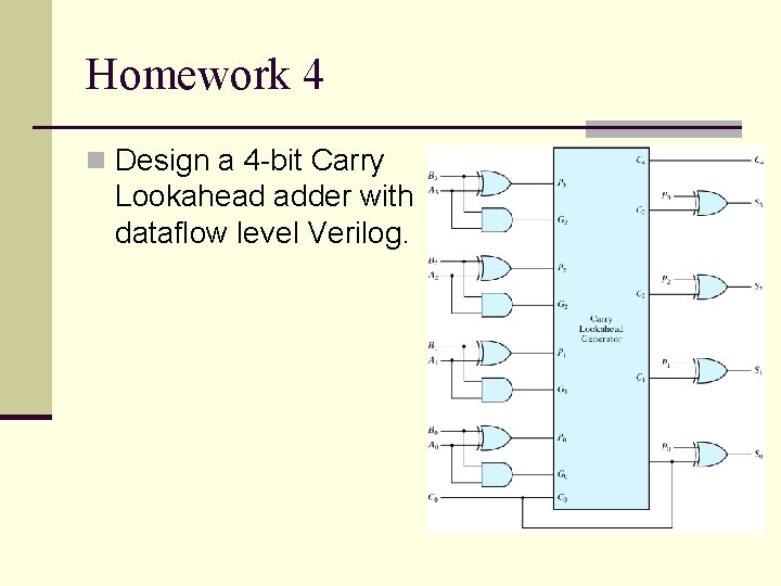
Homework 4 n Design a 4 -bit Carry Lookahead adder with dataflow level Verilog.
- Slides: 17