OUTLINE BASICS K P method and light absorption

OUTLINE ● BASICS: ^ K • P method and light absorption ● Light absorption and carrier dynamics ( , )) ● Intermediate band calculation

The muscling up scheme for understand optical dynamics in semiconductor Fermi’s golden rule The Schrödinger equation ●E-k dispersion ●En and density of states ●Ψ: Wavefunction Absorption coefficient Radiation transition lifetime KP perturbation method Non Radiation transition lifetime Lutinger-Kohn Hamiltonian Electron cooling: Bi-exciton recombination: Plane wave expansion

^ K・P perturbation method : Schrödinge equation Bloch function ^ ^ Note: is not included

K・P^ : Kane model and Luttinger –Kohn model Kane model Luttinger- kohn model Group B S like Group A P like Kane parameter P : K・P Group B L-K parameter: K・P
 are given as:")
^ K・P : Kane model Initial basis set: (electron eigen states) are given as: , (R(r) part will be solved by using K P^ method) S like P like Hamiltonian used for calculation (SO effect included)

Kane model : Explicit form of Hamiltonian Block diagonalisation Kane parameter (predetermined: where: Spin orbit interaction (0. 3~0. 6 e. V): Det(H)=0 Eigenvalue

K・P^ : Kane Model: CB band ● Eg 0 ● HH band LH band Δ ● SO band Energy level (k=0) Wavefunction (k=0)

K・P : Luttinger –Kohn model Hamiltonian: Initial basis set: Following the Löwdin’s renormalization theorem and taking the Kane’s solution at k=0 for valence bands, we write: Löwdin’s perturbation method: Wavefuction of B is included but not included in the calculation. No need to calculate because L-K parameter is used
:")
K・P : Luttinger –Kohn model Explicit form of Hamiltonian: L-K parameter (predetermined):
 In 1 -x.")
K・P : strain effect based on Luttinger –Kohn model (my work) In 1 -x. Gax. As on In. P In_1 -x. Ga_x. As x=0. 3 E-Kx dispersion In_1 -x. Ga_x. As x=0. 3 E-Kz dispersion z z z Kx (Å-1 ) Kz(Å-1 )

K・P : Exercise: strain effect based on Luttinger –Kohn model In_1 -x. Ga_x. As x=0. 4 (reference) PRB, 46 4110 In_1 -x. Ga_x. As x=0. 3 (my work) Kx (Å-1 ) Kz(Å-1 )

K・P : Constant energy contour Unstrained In 1 -x. Gax. As on In. P (x=0. 468) HH Kz (π/a) Kx (π/a) LH Kz (π/a) Kx (π/a)

Transition rate using Fermi’s Golden Rule <b| Absortption Absorption Emission <a| Total transition rate per unit volume Net upward transition rate per unit volume
 ●Wavefunction ●Energy level")
Calculate net transition rate ① ② ③ ④ ⑤ ●H’(r) ●Wavefunction ●Energy level
: electron and photon interaction Light ② (Is not used for calculating")
Origin of H’(r): electron and photon interaction Light ② (Is not used for calculating transition rate) Atom Scale of electric field distribution is too big than atom size Dipole approximation

Momentum matrix elements of bulk and quantum well/dot semiconductor ③ ● CB Eg 0 ● HH LH TE mode: Δ ● SO TM mode:
 ●")
Momentum matrix elements of bulk and quantum well/dot semiconductor Kane parameter (from experiment) ● TE MODE CB Eg 0 Px ● Py HH LH TM MODE Px Py Pz ③

Delta function: ④ =6 =10 =20 =30

Absorption coefficient: Absorption coefficient No. Photons absorbed per unit volume per second = No. Photons injected per unit area per second Momentum transfer matrix
 density of states (JDOS): (1) 3 -D density")
term and Joint (reduced ) density of states (JDOS): (1) 3 -D density of states Conduction band Density of states for electrons Valence band Density of states for hole ①
 density of states (JDOS): (2) CB ● Ef")
term and Joint (reduced ) density of states (JDOS): (2) CB ● Ef with Eg 0 ● reduced electron mass : mr Ei VB Reduced (joint) density of states Under thermal equilibrium Non-equilibrium Carrier concentration difference

Absorption coefficient under thermal equilibrium: Bul. K material CB 3 2. 5 ● Eg 0 2 1. 5 1 ● VB 0. 5 0 0 2 4 6 8 10
")
Light absorption and carrier dynamics ( , tby tomic Stanko)
/Ga. As QD superlattice model ●")
Calculation model: Truncated pyramid Quantum dot In. As (QD)/Ga. As QD superlattice model ● ● ● d=2~10 nm h=2. 5 nm b=10 nm K P plane wave method ●L-K hamiltonian ●Fourier transformation ● ● ●

Charge density contour and band dispersion Quantum dot array Single Quantum do Ga. As In. As h 0 e 0 e 2 e 1 e 0
/Ga. As Absorption")
Absorption : IB=>CB Band structure and Potential profile of In. As (QD)/Ga. As Absorption spectrum (cm-1) Shape anisotropy and polarization Barrier Continuum e 0 e 2 e 0 e 1 Bragg type confinment miniband ① ② e 2 e 1 , e 2 band : p like TE ① ③ ② ---TE mode ---TM mode Px TM e 0 ● ● ③ IB=> CB transition Py Pz Due to shape anisotropy, QD is more TE polarized
/Ga. As Absorption")
Absorption : VB=>IB Band structure and Potential profile of In. As (QD)/Ga. As Absorption spectrum Polarization dependence (cm-1) 5 x 10⁴ Due to highly biaxial compressive strain and the hydrostatic component makes h 0 state heavy hole character. Barrier Continuum e 2 HH e 1 Px e 0 TE ① ② h 0 ① ● ● ② ③ ● ● ③ VB=> IB transition TM Py
")
VB=>CB transition and many body effect VB=> CB transition Sommerfeld factor (absorption enhance effect) Barrier Continuum e 2 e 1 Sommerfeld factor get extremely large at band edge ① e 0 h 0 ① Band edge E (e. V) ● Many body effect (Coublum interaction) is not important because exciton is almost ionized , but it becomes pronounced when at low temperature.
 ● Life time depends on energy difference Single QD QD")
Radiative transition times (radiative recombination) ● Life time depends on energy difference Single QD QD SL(Kz=0) 149 ns 109 ns 129 ns 98 ● Life time depends on moment um matrix e 1, e 2 =>e 0 (intraband transition) =52 e 0=>h 0 (inter band transition) Single QD QD SL(Kz=0) 1. 59 ns 2. 1 ns

Auger recombination: electron cooling Coulomb integral Single In. As QD SL

Auger recombination: biexiciton recombination biexiciton Single QD QD SL

Electron phonon interaction: absorption and emission Absorption Emission V e 6 m 3 e 1 -e 0

Summary: ① Radiative recombination. CB=>IB ② Radiative recombination. IB=>VB ③ Phonon emission assisted CB=>IB ④ Phonon absorption assisted IB=>CB ⑤ Auger electron cooling between CB=>IB ⑥ Auger biexciton relaxation between IB=>VB

Appendix: Kronig-Penny Model

Ga. As/Alx. Ga 1 -x. As quantum well superlattice band calculation: Well width Barrier width Al 0. 3 Ga 0. 7 As ΔEc Al 0. 3 Ga 0. 7 As Eg1 Ga As Eg 2 Ga As ΔEv 井戸幅(ドット直径) バリア層幅 Eg1 Eg 2 ΔEC ΔEv 2 nm-30 nm 2 nm-10 nm 1. 424 e. V 1. 80 e. V 0. 25 e. V 0. 125 e. V Calculation method: Transfer matrix method
 C")
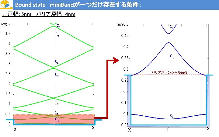
Bound state & Continuum mini. Band 井戸幅: 10 nm バリア層幅 4 nm (e. V) C 8 C 1 C 7 C 6 バリアポテンシャル(e. V) B 2 C 5 C 4 B 1 C 3 C 2 B 0 C 1 Х Г Х
 バリア層幅 4 nm バリア層幅 2 nm B B")
伝導帯Bound miniband の障壁幅/井戸幅依存性 : (e. V) バリア層幅 4 nm バリア層幅 2 nm B B 62 B 4 井戸幅: 10 nm, 20 nm , 30 nm バリア層幅 8 nm B 2 B 4 B 6 B 5 B 3 B 4 B 1 B B 12 Х Г Х B 2 井戸幅: 10 nm, 20 nm , 30 nm B 5 B 3 B 4 B 1 B 2 B 3 B 2 B 1 B 0 B 0 B 3 B 2 B 0 B 1 B 0 B 0 B 2 B 1 B 0 Х Г B 2 B 4 B 6 井戸幅: 10 nm, 20 nm , 30 nm B 5 B 2 B 4 B 6 バリア層幅 10 nm Х Х Г Х
 バリア層幅 2 nm LH 0 バリア層幅")
Light hole Bound miniband の障壁幅/井戸幅依存性 : (e. V) バリア層幅 2 nm LH 0 バリア層幅 4 nm LH 0 LH 1 LH 2 LH 1 井戸幅: 10 nm, 20 nm , 30 nm LH 2 LH 3 LH 4 LH 0 井戸幅: 10 nm, 20 nm , 30 nm バリア層幅 8 nm バリア層幅 10 nm LH 0 LH 1 LH 0 LH 1 LH 2 井戸幅: 10 nm, 20 nm , 30 nm LH 2 LH 3 LH 2 LH 4 LH 1 LH 4 LH 3 LH 1 LH 3
 バリア層幅:")
伝導帯 miniband & 価電子帯 miniband: 井戸幅: 4 nm バリア層幅: 4 nm (e. V) バリア層幅: 4 nm 井戸幅: 20 nm (e. V) B 3 B 2 B 0 B 1 B 0 HH 0 LH 0 HH 1 LH 0 HH 0 LH 1 HH 2 LH 2 HH 3 HH 4 LH 3
- Slides: 41