Optoelectronics Materials An Introduction Outline Introduction Basic Aspects
Optoelectronics Materials (An Introduction) 무니르
Outline Introduction Basic Aspects Properties of lights Structure of materials Electrical properties of semiconductor Optical properties of semiconductor Light Detection and Imaging Photo-detectors Charged Couple Devices (CCD)

Fiber optic Optoelectronics? Opto ~ optics, lights, photons Electronic ~ involves electron movements Optoelectronics “converts light into electricity” Applications: LED Optical storage (CD, DVD) Communications (fiber optics) Imaging/Display (CRT, LCD, TFT) Publishing (Laser printer) Guidance and control (Laser devices) Env. energy supply (Solar cell) Health (Painless therapy) Defense (Night vision - military) More……. . Solar-powered PDA Display Frame
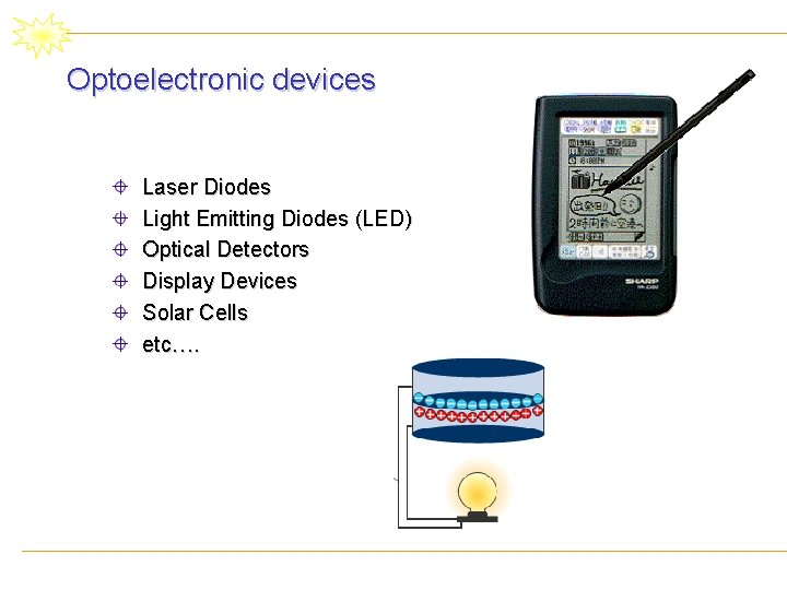
Optoelectronic devices Laser Diodes Light Emitting Diodes (LED) Optical Detectors Display Devices Solar Cells etc….
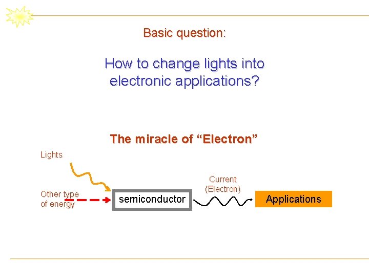
Basic question: How to change lights into electronic applications? The miracle of “Electron” Lights Other type of energy semiconductor Current (Electron) Applications
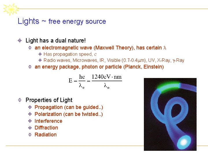
Lights ~ free energy source Light has a dual nature! an electromagnetic wave (Maxwell Theory), has certain Has propagation speed, c Radio waves, Microwaves, IR, Visible (0. 7 -0. 4 m), UV, X-Ray, -Ray an energy package, photon or particle (Planck, Einstein) Properties of Light Propagation (can be guided. . ) Polarization (can be twisted. . ) Interference Diffraction Radiation
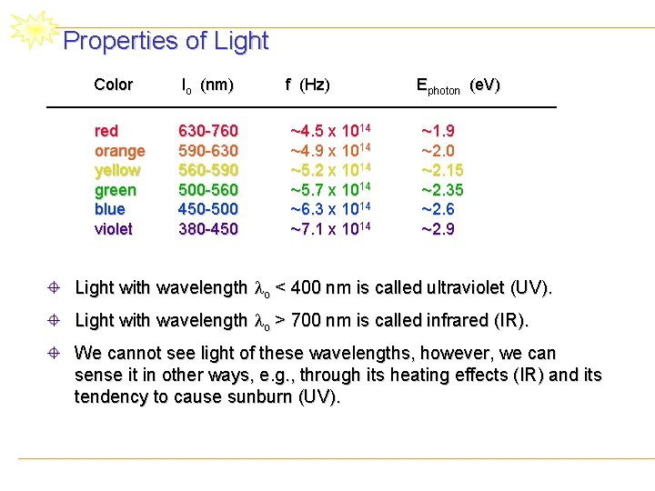
Properties of Light Color red orange yellow green blue violet lo (nm) 630 -760 590 -630 560 -590 500 -560 450 -500 380 -450 f (Hz) ~4. 5 x 10¹⁴ ~4. 9 x 10¹⁴ ~5. 2 x 10¹⁴ ~5. 7 x 10¹⁴ ~6. 3 x 10¹⁴ ~7. 1 x 10¹⁴ Ephoton (e. V) ~1. 9 ~2. 0 ~2. 15 ~2. 35 ~2. 6 ~2. 9 Light with wavelength o < 400 nm is called ultraviolet (UV). Light with wavelength o > 700 nm is called infrared (IR). We cannot see light of these wavelengths, however, we can sense it in other ways, e. g. , through its heating effects (IR) and its tendency to cause sunburn (UV).
Basic Materials Structure Solids Crystalline: periodicity, Long Range Order (LRO) Polycrystalline: LRO several microns Amorphous: good SRO, no LRO Liquid and Gaseous No ordering Can flow and take the container’s shape Liquid Crystal (Organic) LRO Flow of atoms/molecules Has both properties of solid crystalline and liquid
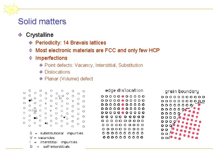
Solid matters Crystalline Periodicity: 14 Bravais lattices Most electronic materials are FCC and only few HCP Imperfections Point defects: Vacancy, Interstitial, Substitution Dislocations Planar (Volume) defect
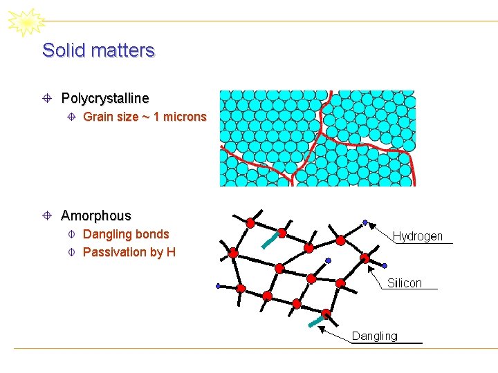
Solid matters Polycrystalline Grain size ~ 1 microns Amorphous Dangling bonds Passivation by H
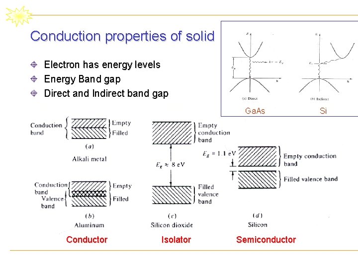
Conduction properties of solid Electron has energy levels Energy Band gap Direct and Indirect band gap Ga. As Conductor Isolator Semiconductor Si
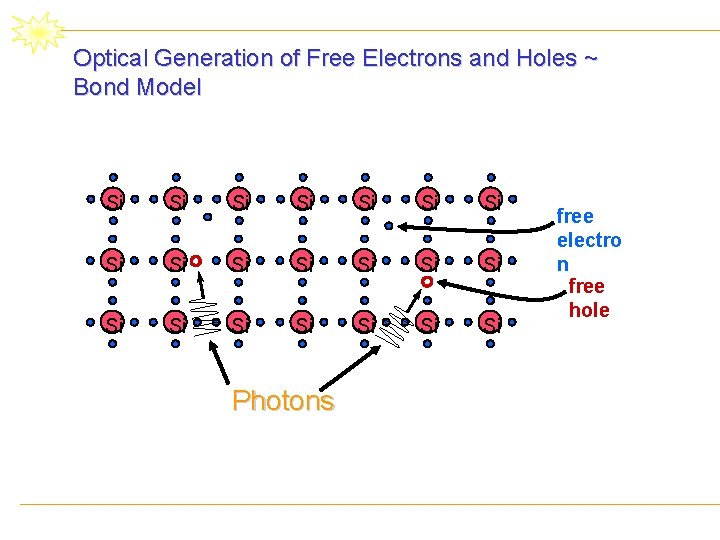
Optical Generation of Free Electrons and Holes ~ Bond Model Si Si Si Si Si Si Photons free electro n free hole
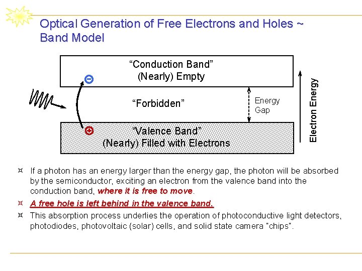
“Conduction Band” (Nearly) Empty “Forbidden” “Valence Band” (Nearly) Filled with Electrons Energy Gap Electron Energy Optical Generation of Free Electrons and Holes ~ Band Model ³ If a photon has an energy larger than the energy gap, the photon will be absorbed by the semiconductor, exciting an electron from the valence band into the conduction band, where it is free to move. ³ A free hole is left behind in the valence band. ³ This absorption process underlies the operation of photoconductive light detectors, photodiodes, photovoltaic (solar) cells, and solid state camera “chips”.
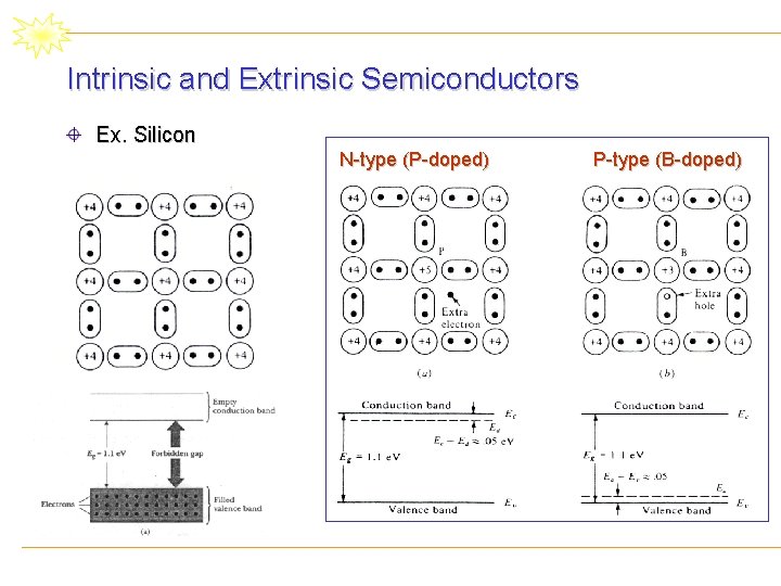
Intrinsic and Extrinsic Semiconductors Ex. Silicon N-type (P-doped) P-type (B-doped)
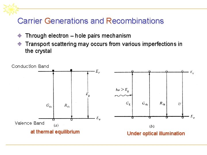
Carrier Generations and Recombinations Through electron – hole pairs mechanism Transport scattering may occurs from various imperfections in the crystal Conduction Band Valence Band at thermal equilibrium Under optical illumination
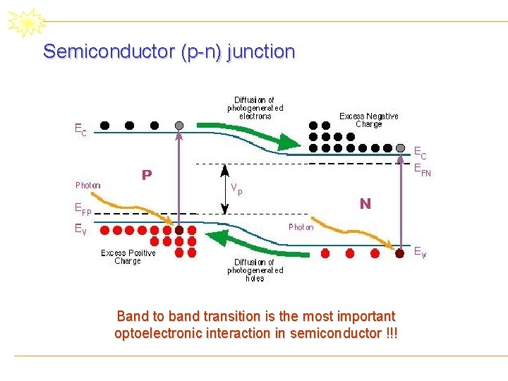
Semiconductor (p-n) junction Band to band transition is the most important optoelectronic interaction in semiconductor !!!
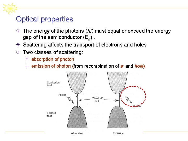
Optical properties The energy of the photons (hf) must equal or exceed the energy gap of the semiconductor (Eg). Scattering affects the transport of electrons and holes Two classes of scattering: absorption of photon emission of photon (from recombination of e- and hole)
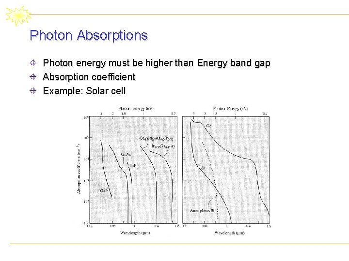
Photon Absorptions Photon energy must be higher than Energy band gap Absorption coefficient Example: Solar cell
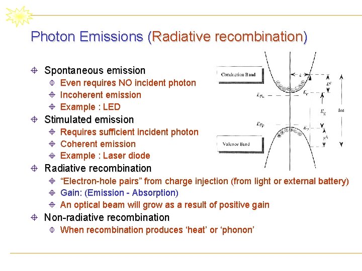
Photon Emissions (Radiative recombination) Spontaneous emission Even requires NO incident photon Incoherent emission Example : LED Stimulated emission Requires sufficient incident photon Coherent emission Example : Laser diode Radiative recombination “Electron-hole pairs” from charge injection (from light or external battery) Gain: (Emission - Absorption) An optical beam will grow as a result of positive gain Non-radiative recombination When recombination produces ‘heat’ or ‘phonon’
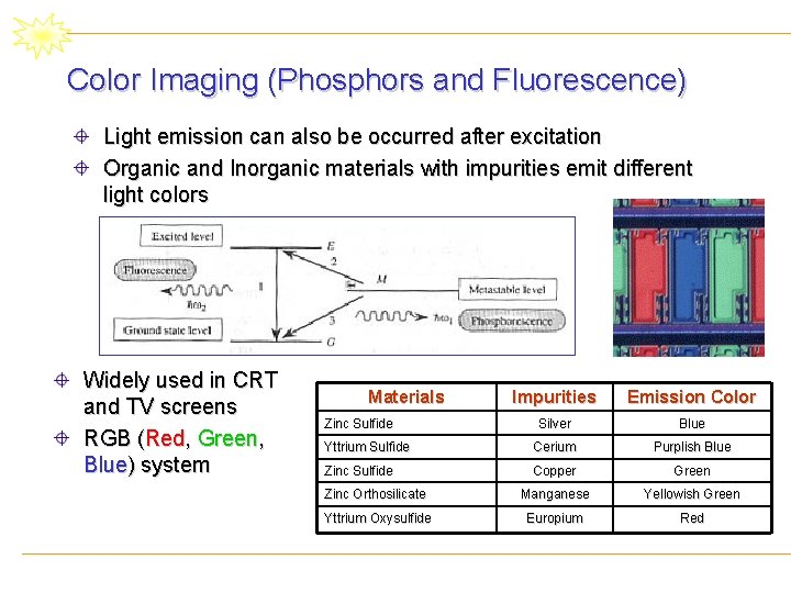
Color Imaging (Phosphors and Fluorescence) Light emission can also be occurred after excitation Organic and Inorganic materials with impurities emit different light colors Widely used in CRT and TV screens RGB (Red, Green, Blue) system Materials Impurities Emission Color Silver Blue Yttrium Sulfide Cerium Purplish Blue Zinc Sulfide Copper Green Zinc Orthosilicate Manganese Yellowish Green Yttrium Oxysulfide Europium Red Zinc Sulfide
Outline Introduction Basic Aspects Properties of lights Structure of materials Electrical properties of semiconductor Optical properties of semiconductor Light Detection and Imaging Photodetectors Charged Couple Devices (CCD)
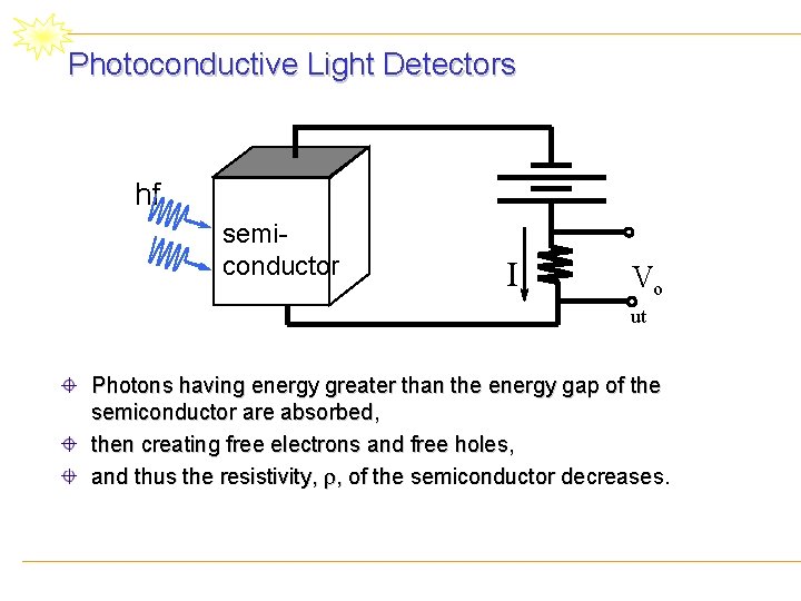
Photoconductive Light Detectors hf semiconductor I Vo ut Photons having energy greater than the energy gap of the semiconductor are absorbed, then creating free electrons and free holes, and thus the resistivity, r, of the semiconductor decreases.
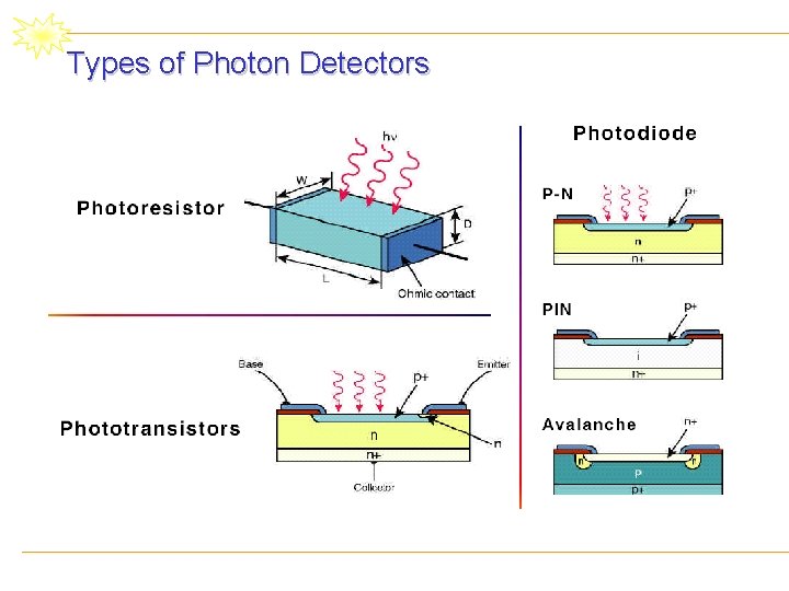
Types of Photon Detectors
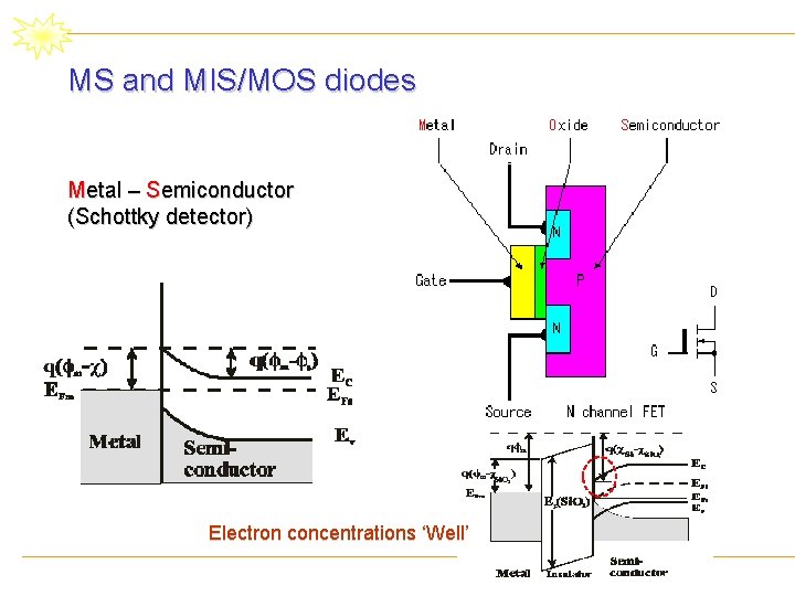
MS and MIS/MOS diodes Metal – Semiconductor (Schottky detector) Electron concentrations ‘Well’
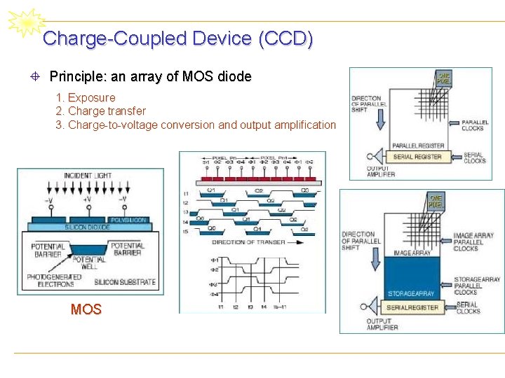
Charge-Coupled Device (CCD) Principle: an array of MOS diode 1. Exposure 2. Charge transfer 3. Charge-to-voltage conversion and output amplification MOS
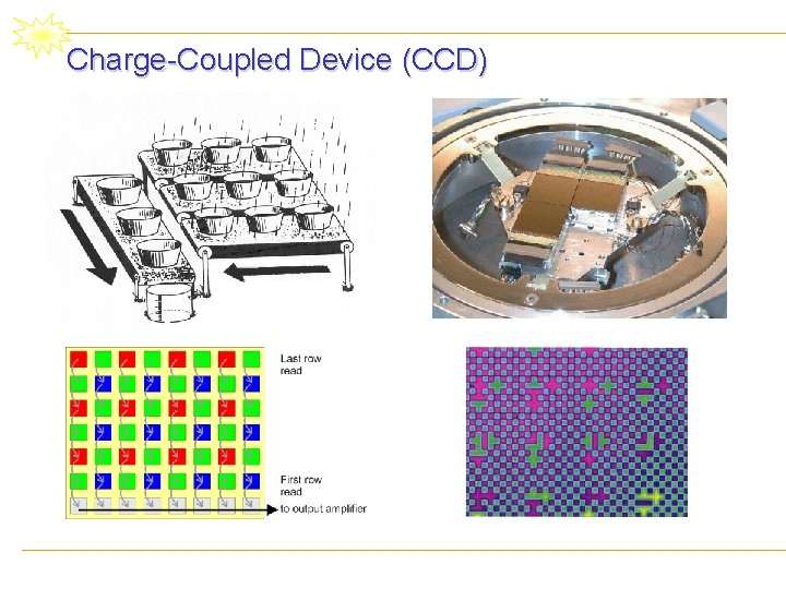
Charge-Coupled Device (CCD)
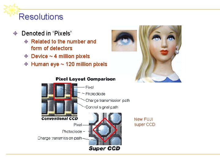
Resolutions Denoted in ‘Pixels’ Related to the number and form of detectors Device ~ 4 million pixels Human eye ~ 120 million pixels New FUJI super CCD
Outline Introduction Basic Aspects Properties of lights Structure of materials Electrical properties of semiconductor Optical properties of semiconductor Light Detection and Imaging Photodetectors Charged Couple Devices (CCD)
Concluding remarks: light and electron
- Slides: 29