Optoelectronic MultiChip Module Demonstrator System Jason D Bakos
Optoelectronic Multi-Chip Module Demonstrator System Jason D. Bakos Donald M. Chiarulli, Steven P. Levitan University of Pittsburgh, USA
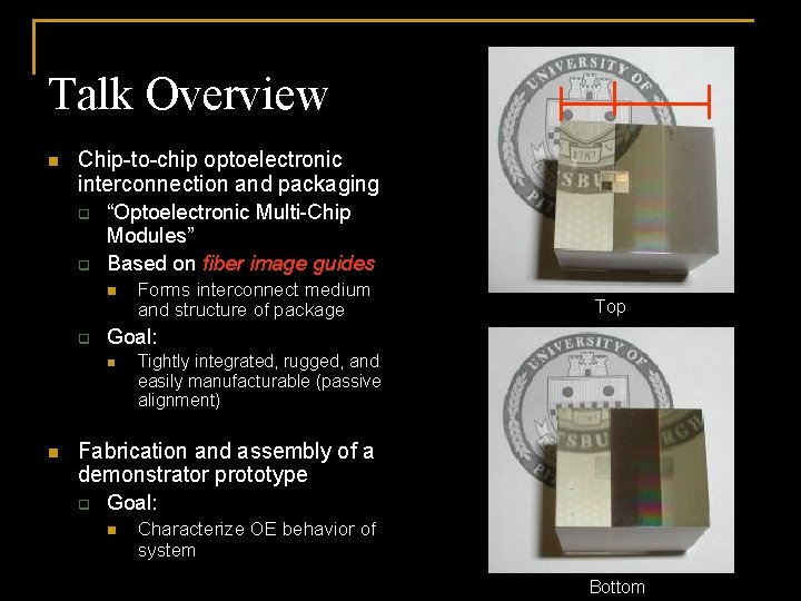
Talk Overview n Chip-to-chip optoelectronic interconnection and packaging q q “Optoelectronic Multi-Chip Modules” Based on fiber image guides n q Top Goal: n n Forms interconnect medium and structure of package Tightly integrated, rugged, and easily manufacturable (passive alignment) Fabrication and assembly of a demonstrator prototype q Goal: n Characterize OE behavior of system Bottom

OE-MCM Demonstrator System n 64 -channel optical crossbar switch as 3 -element OE-MCM Each identical element q q q n Has 8 x 8 array of detectors and VCSELs at 250 um Implements eight independent 8 -channel switches (“rows”) Each chip aligned orthogonal to its adjacent chip 2 D fiber ribbon cable (8 x 8) carries optical data in/out of MCM FIG Chip 1 FIG Chip 2 FIG Chip 3 FIG 2 D fiber ribbon cable n 3 -stage switch architecture

OE-MCM Interconnect Topology IN Chip 2 OUT Chip 1 Chip 3 Chip 2 Chip 3 Chip 1

OE-MCM Fabrication and Bonding n n Digital/analog on CMOS chip Flip-chip bond OE chips to CMOS die Epoxy assembled elements to sides of image guide glass Bump-bond CMOS chips to PCB (supplies, electronic I/O) Assembled “switch chip” 8 x 8 channel array MCM cross section
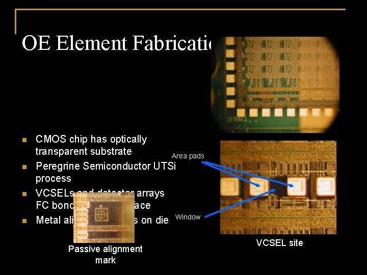
OE Element Fabrication n n CMOS chip has optically transparent substrate Area pads Peregrine Semiconductor UTSi process VCSELs and detector arrays FC bonded to top surface Metal alignment marks on die Window Passive alignment mark VCSEL site
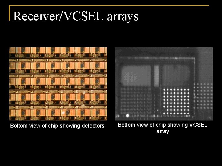
Receiver/VCSEL arrays Bottom view of chip showing detectors Bottom view of chip showing VCSEL array
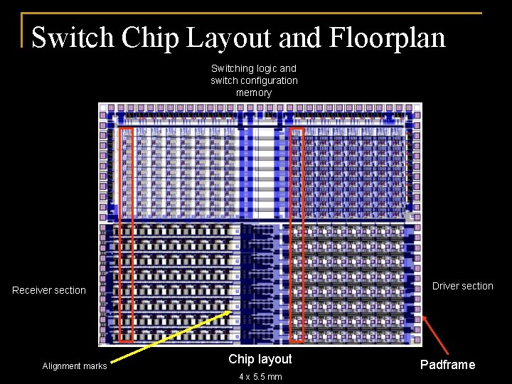
Switch Chip Layout and Floorplan Switching logic and switch configuration memory Driver section Receiver section Alignment marks Chip layout 4 x 5. 5 mm Padframe
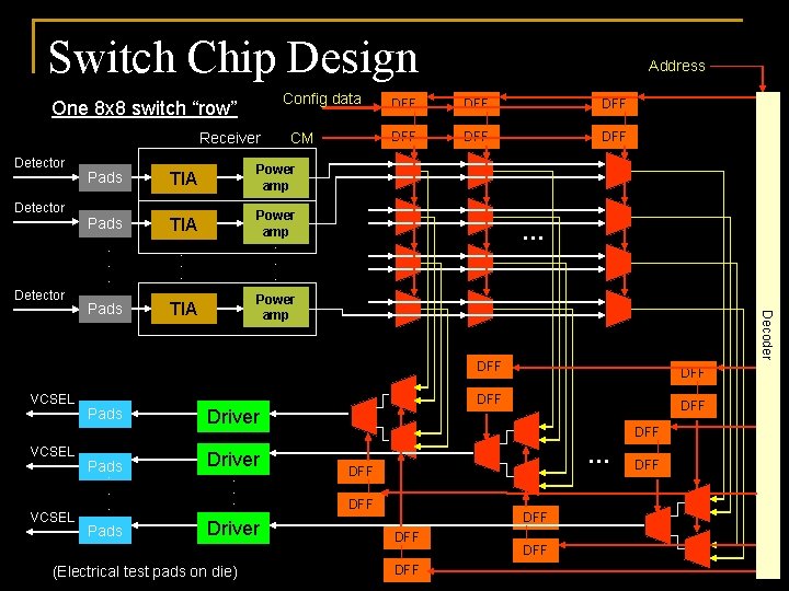
Switch Chip Design Config data One 8 x 8 switch “row” Receiver Detector Pads TIA Power amp Detector. . . Detector VCSEL Pads. . VCSEL . Pads DFF DFF DFF … . . . Power amp TIA Driver. . . Driver (Electrical test pads on die) Decoder VCSEL CM Address DFF DFF DFF … DFF DFF
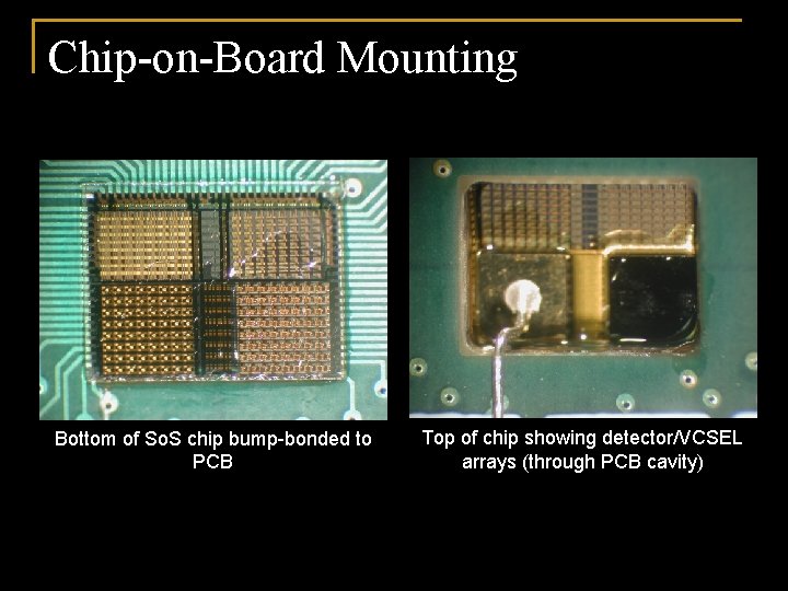
Chip-on-Board Mounting Bottom of So. S chip bump-bonded to PCB Top of chip showing detector/VCSEL arrays (through PCB cavity)
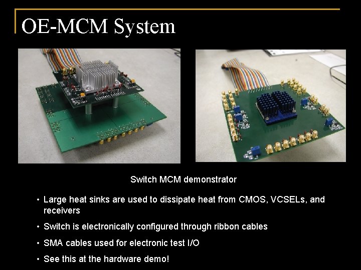
OE-MCM System Switch MCM demonstrator • Large heat sinks are used to dissipate heat from CMOS, VCSELs, and receivers • Switch is electronically configured through ribbon cables • SMA cables used for electronic test I/O • See this at the hardware demo!
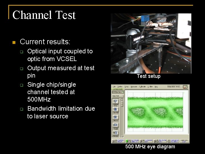
Channel Test n Current results: q q Optical input coupled to optic from VCSEL Output measured at test pin Single chip/single channel tested at 500 MHz Bandwidth limitation due to laser source Test setup 500 MHz eye diagram
Conclusion and Future Work n FIG-based OE-MCMs q q n FIG: interconnect medium and structure Tightly integrated and easily manufacturable Fabrication and characterization of OE-MCM demonstrator q q Currently in progress Proof-of-concept for FIG-based OE-MCM technology
Acknowledgements n Thank you: q So. S COOP run n q Peregrine Semiconductor n q UTSi fab run Bonding and support Schott Fiber Optics n Fiber image guides and support
- Slides: 14